

Page 1

MAX2690
Low-Noise, 2.5GHz
Downconverter Mixer
________________________________________________________________
Maxim Integrated Products
1
19-1282; Rev 0; 10/97
EVALUATION KIT
AVAILABLE
For free samples & the latest literature: http://www.maxim-ic.com, or phone 1-800-998-8800.
For small orders, phone 408-737-7600 ext. 3468.
_______________General Description
The MAX2690 is a miniature, low-noise, low-power
downconverter mixer designed for use in portable consumer equipment. Signals at the RF input port are
mixed with signals at the local-oscillator (LO) port using
a double-balanced mixer. The RF port frequency range
is 400MHz to 2500MHz. The LO port frequency range is
700MHz to 2500MHz. The IF frequency range is 10MHz
to 500MHz, provided the LO and RF frequencies are
chosen appropriately.
The IF port is differential, which provides good linearity
and low LO emissions, as well as providing compatibility with applications using differential IF filters, such as
CDMA cellular phones. The mixer noise figure is 10dB
at 900MHz.
The MAX2690 draws 16mA at VCC= 3V and operates
from a +2.7V to +5.5V supply. A logic-controlled shutdown mode reduces the supply current to less than 1µA,
making it ideal for battery-operated equipment. This
device is offered in a miniature 10-pin µMAX package.
________________________Applications
2.45GHz Industrial-Scientific-Medical (ISM)
Band Radios
Wireless Local Area Networks (WLANs)
Personal Communications Systems (PCS)
Code-Division Multiple Access (CDMA)
Communications Systems
Cellular and Cordless Phones
Hand-Held Radios
____________________________Features
♦ 7.6dBm Input Third-Order Intercept Point
♦ 10dB Downconverter Mixer Noise Figure
♦ 7.9dB Gain
♦ 400MHz to 2500MHz Wideband Operation
♦ Low Cost
♦ +2.7V to +5.5V Single-Supply Operation
♦ <1µA Shutdown Mode
♦ Ultra-Small 10-Pin µMAX Package
PART
MAX2690EUB -40°C to +85°C
TEMP. RANGE PIN-PACKAGE
10 µMAX
______________Ordering Information
__________________Pin Configuration
1
2
3
4
5
10
9
8
7
6
SHDN
IFOUT+
IFOUTGNDLORFBYP
RFIN
GND
LGND
MAX2690
µMAX
TOP VIEW
LOV
CC
________________Functional Diagram
1
2
3
4
5
10
9
8
7
6
SHDN
IFOUT+
IFOUTGNDLORFBYP
RFIN
GND
LGND
MAX2690
µMAX
TOP VIEW
LOV
CC
BIAS
Typical Operating Circuit appears at end of data sheet.
Page 2

MAX2690
Low-Noise, 2.5GHz
Downconverter Mixer
2 _______________________________________________________________________________________
ABSOLUTE MAXIMUM RATINGS
DC ELECTRICAL CHARACTERISTICS
(VCC= +2.7V to +5.5V, no RF signals applied, LO = open, IFOUT+ = IFOUT- = VCC, SHDN = high, LGND = GND = GNDLO = 0V,
T
A
= T
MIN
to T
MAX
. Typical values are at VCC= +3.0V and TA= +25°C, unless otherwise noted. Minimum and maximum values are
guaranteed by design and characterization over temperature.)
AC ELECTRICAL CHARACTERISTICS
(MAX2690 EV kit; VCC= +3.0V; PLO= -3dBm; PRF= -25dBm; SHDN = high; RFIN matched for 900MHz, 1.95GHz, and 2.45GHz as
noted below. Inductor connected from LGND to GND = 39nH for 900MHz operation, 27nH for 1.95GHz operation, and 6.8nH for
2.45GHz operation. T
A
= +25°C, unless otherwise noted.)
Stresses beyond those listed under “Absolute Maximum Ratings” may cause permanent damage to the device. These are stress ratings only, and functional
operation of the device at these or any other conditions beyond those indicated in the operational sections of the specifications is not implied. Exposure to
absolute maximum rating conditions for extended periods may affect device reliability.
VCCto GND...........................................................-0.3V to +6.0V
RFIN Input Power..............................................................10dBm
LO Input Power.................................................................10dBm
SHDN Input Voltage...................................-0.3V to (V
CC
+ 0.3V)
Continuous Power Dissipation
10-Pin µMAX (derate 4.1mW/°C above +70°C)............330mW
Operating Temperature Range
MAX2690EUB...................................................-40°C to +85°C
Junction Temperature......................................................+150°C
Storage Temperature Range.............................-65°C to +165°C
Lead Temperature (soldering, 10sec).............................+300°C
SHDN = 0V
SHDN = low
0V < SHDN < V
CC
CONDITIONS
V0.5Shutdown Input Voltage Low
V2
mA9.5 16 20.1Operating Supply Current
Shutdown Input Voltage High
0.4
µA
2
Shutdown Supply Current
µA-5 4 25Shutdown Input Bias Current
UNITSMIN TYP MAXPARAMETER
fRF= 2.45GHz, fLO= 2.1GHz
fRF= 1.95GHz, fLO= 1.75GHz
fRF= 900MHz, fLO= 1.1GHz
fRF= 1.95GHz, TA= T
MIN
to T
MAX
(Note 2)
CONDITIONS
dB
4
6.4
7.9
Conversion Gain
(Note 1)
dB±0.6 ±1.2
Gain Variation over
Temperature
UNITSMIN TYP MAXPARAMETER
Two tones at
-25dBm per tone,
f
RF2
= 1MHz above f
RF
fRF= 900MHz, fLO= 1.1GHz
dBm
4.3
5.3
7.6
Input Third-Order Intercept
10
fRF= 2.45GHz, fLO= 2.1GHz
fRF= 1.95GHz, fLO= 1.75GHz
dB
12
Noise-Figure
Single Sideband
11.5
fRF= 900MHz, fLO= 1.1GHz
fRF= 1.95GHz, fLO= 1.75GHz
fRF= 2.45GHz, fLO= 2.1GHz
Page 3

MAX2690
Low-Noise, 2.5GHz
Downconverter Mixer
_______________________________________________________________________________________ 3
AC ELECTRICAL CHARACTERISTICS (continued)
(MAX2690 EV kit; VCC= +3.0V; PLO= -3dBm; PRF= -25dBm; SHDN = high; RFIN matched for 900MHz, 1.95GHz, and 2.45GHz as
noted below. Inductor connected from LGND to GND = 39nH for 900MHz operation, 27nH for 1.95GHz operation, and 6.8nH for
2.45GHz operation. T
A
= +25°C, unless otherwise noted.)
Note 1: Consult the
Applications Information
section for information on designing a matching network.
Note 2: Guaranteed by design and characterization.
Note 3: This spurious response is caused by a higher-order mixing product (2x2). Specified RF frequency is applied and IF output
power is observed at the desired IF frequency (200MHz for f
RF
= 900MHz, or 1.95GHz, and 350MHz for fRF= 2.45GHz).
Note 4: From the time SHDN goes high to the time I
CC
reaches 90% of its final value (on), or from the time SHDN goes low to the
time I
CC
drops below 10µA (off).
fRF= 2.45GHz, fLO= 2.1GHz
fRF= 1.95GHz, fLO= 1.75GHz
fRF= 900MHz, fLO= 1.1GHz
-74
RF input = -15dBm
(Note 4)
dBm
CONDITIONS
-56
IF/2 Spurious Response
(Note 3)
-62
µs1Turn-On Time
dBm
-28
-32
-32
LO Emission at IF Port
UNITSMIN TYP MAXPARAMETER
fRF= 2.45GHz, fLO= 2.1GHz
fRF= 1.95GHz, fLO= 1.75GHz
fRF= 900MHz, fLO= 1.1GHz
dBm
-25
-27
-30
LO Emission at RF Port
(Note 4) µs1.6Turn-Off Time
fRF= 1.0GHz, fLO= 1.1GHz
fRF= 1.85GHz, fLO= 1.75GHz
fRF= 2.275GHz, fLO= 2.1GHz
Page 4

MAX2690
Low-Noise, 2.5GHz
Downconverter Mixer
4 _______________________________________________________________________________________
__________________________________________Typical Operating Characteristics
(MAX2690 EV kit, VCC= +3.0V, PLO= -3dBm, PRF= -25dBm, fRF= 1.95GHz, fIF= 200MHz, SHDN = high, TA= +25°C, unless
otherwise noted.)
5
9
7
13
11
17
15
19
23
21
25
2.7 3.3 3.6 3.93.0 4.2 4.5 4.8 5.45.1 5.7
SUPPLY CURRENT
vs. SUPPLY VOLTAGE
MAX2690toc01
SUPPLY VOLTAGE (V)
SUPPLY CURRENT (mA)
TA = +25°C
T
A
= -40°C
TA = +85°C
0
0.4
0.2
0.6
1.2
1.4
1.0
0.8
1.6
2.7 3.3 3.6 3.9 4.23.0 4.5 4.8 5.1 5.4 5.7
SHUTDOWN SUPPLY CURRENT
vs. SUPPLY VOLTAGE
MAX2690toc02
SUPPLY VOLTAGE (V)
SHUTDOWN SUPPLY CURRENT (µA)
TA = +25°C
T
A
= -40°C
TA = +85°C
SHDN = 0V
4.0
4.6
4.4
4.2
4.8
5.0
5.2
5.4
5.6
5.8
6.0
50 150100 200 250 300 350
CONVERSION GAIN
vs. IF FREQUENCY
MAX2690toc03
IF FREQUENCY (MHz)
CONVERSION GAIN (dB)
fRF = 2.45GHz
-6
-4
-2
0
2
4
6
8
10
0 1000500 1500 2000 2500 3000
CONVERSION GAIN
vs. RF FREQUENCY
MAX2690toc04
RF FREQUENCY (MHz)
CONVERSION GAIN (dB)
fIF = 200MHz
fIF = 200MHz
fIF = 350MHz
-6
-2
-4
0
6
8
4
2
10
-15 -11 -9 -7 -5-13 -3 -1 1 3 5
CONVERSION GAIN
vs. LO POWER
MAX2690toc07
LO POWER (dBm)
GAIN (dB)
fRF = 900MHz, fIF = 200MHz
fRF = 1950MHz, fIF = 200MHz
fRF = 2450MHz, fIF = 350MHz
0
4
2
8
6
12
10
14
500 15001000 2000 2500 3000
NOISE FIGURE
vs. RF FREQUENCY AND TEMPERATURE
MAX2690toc05
RF FREQUENCY (MHz)
NOISE FIGURE (dB)
900
1950
2450
f
RF
(MHz)
f
IF
(MHz)
200
200
350
TA = +85°C
TA = +25°C
TA = -40°C
0
40
20
80
60
120
100
140
-350
-250
-300
-150
-200
-50
-100
0
500 1000 1500 2000 2500
RF PORT IMPEDANCE
vs. FREQUENCY
MAX2690toc06
FREQUENCY (MHz)
REAL IMPEDANCE (Ω)
IMAGINARY IMPEDANCE (Ω)
IMAGINARY
REAL
-50
-40
-30
-10
-20
0
10
0 0.6 0.9 1.20.3 1.5 1.8 2.1 2.72.4 3.0
LO PORT S11 vs. FREQUENCY
MAX2690toc09
FREQUENCY (GHz)
LO PORT S11 (dB)
0
4
2
8
6
12
10
14
0 12 27 47
GAIN AND LINEARITY
vs. LGND INDUCTOR VALUE
MAX2690toc08
LGND INDUCTOR VALUE (nH)
GAIN AND LINEARITY (dB or dBm)
fRF = 1.95GHz
GAIN
IIP3
OIP3
Page 5

MAX2690
Low-Noise, 2.5GHz
Downconverter Mixer
_______________________________________________________________________________________
5
4.0
5.0
4.5
6.0
5.5
7.0
6.5
7.5
8.5
8.0
9.0
900 1300 1700 2100 2500
IIP3 vs.
RF FREQUENCY AND TEMPERATURE
MAX2690toc10
RF FREQUENCY (MHz)
INPUT THIRD-ORDER INTERCEPT (dBm)
TA = +25°C
T
A
= -40°C
TA = +85°C
f
RF2
= 1MHz ABOVE f
RF
0
4
2
10
8
6
16
14
12
18
0
1.0
0.5
2.5
2.0
1.5
4.0
3.5
3.0
4.5
1 250125 375 500
SINGLE-ENDED IF PORT EQUIVALENT
SHUNT RC NETWORK
MAX2690toc11
FREQUENCY (MHz)
RESISTANCE (kΩ)
CAPACITANCE (pF)
CAPACITANCE
RESISTANCE
-100
-80
-90
-70
-40
-30
-50
OUTPUT POWER (dBm)
-60
-20
0 0.6 0.9 1.2 1.50.3 1.8 2.1 2.4 2.7 3.0
IF PORT OUTPUT SPECTRUM
MAX2690toc12
FREQUENCY (GHz)
fRF = 900MHz
IF = 200MHz
LO = 1.1GHz
2LO
3LO - RF
2LO - RF
LO + RF
RF
-8
-6
-7
-4
-5
-3
-2
500 15001000 2000 2500 3000
INPUT 1dB COMPRESSION vs.
RF FREQUENCY AND TEMPERATURE
MAX2690toc13
RF FREQUENCY (MHz)
INPUT 1dB COMPRESSION (dBm)
TA = +85°C
T
A
= +25°C
T
A
= -40°C
900
1950
2450
f
RF
(MHz)
f
IF
(MHz)
200
200
350
0
2
1
4
3
6
5
7
9
8
10
2.0 3.0 3.52.5 4.0 4.5 5.0 5.5 6.0
CONVERSION GAIN
vs. SUPPLY VOLTAGE
MAX2690toc14
V
CC
(V)
CONVERSION GAIN (dB)
fRF = 900MHz, fIF = 200MHz
fRF = 1.95GHz, fIF = 200MHz
fRF = 2.95GHz, fIF = 350MHz
0
2
1
4
3
6
5
7
9
8
10
2.0 3.0 3.52.5 4.0 4.5 5.0 5.5 6.0
INPUT IP3 vs. SUPPLY VOLTAGE
MAX2690toc15
V
CC
(V)
INPUT IP3 (dBm)
fRF = 900MHz, fIF = 200MHz
fRF = 2450MHz, fIF = 350MHz
f
RF
= 1950MHz, f
IF
= 200MHz
0
2
1
5
4
3
8
7
6
9
-40 0 20-20 40 60 80 100
CONVERSION GAIN
vs. TEMPERATURE
MAX2690toc16
TEMPERATURE (°C)
CONVERSION GAIN (dB)
fRF = 900MHz, fIF = 200MHz
fRF = 1950MHz, fIF = 200MHz
fRF = 2450MHz, fIF = 350MHz
____________________________Typical Operating Characteristics (continued)
(MAX2690 EV kit, VCC= +3.0V, PLO= -3dBm, PRF= -25dBm, fRF= 1.95GHz, fIF= 200MHz, SHDN = high, TA= +25°C, unless
otherwise noted.)
Page 6

MAX2690
Low-Noise, 2.5GHz
Downconverter Mixer
6 _______________________________________________________________________________________
________________________________________________Key Specification Statistics
(MAX2690 EV kit, VCC= +3.0V, PLO= -3dBm, PRF= -25dBm, fRF= 1.95GHz, fIF= 200MHz, SHDN = high, TA= +25°C, unless otherwise noted.) Histograms represent measured data from a 30-unit sample taken from one wafer lot. The Gaussian curve is calculated for the measured data’s mean and standard deviation and is scaled to account for process variations (the listed mean and
standard deviation are from the scaled distribution, as plotted).
0
0.4
0.2
0.8
0.6
1.0
1.2
0
6
3
12
9
15
18
3.0 3.8 4.6 5.4 6.2 7.0 7.8
GAIN (+85°C)
MAX2690toc17
GAIN (dB)
PROBABILITY DENSITY FUNCTION
N0. OF UNITS
x = 5.76dB
σ = 0.338dB
0
0.4
0.2
0.8
0.6
1.0
1.2
0
6
3
12
9
15
18
3.4 4.2 5.0 5.8 6.6 7.4
INPUT IP3 (+85°C)
MAX2690toc18
INPUT IP3 (dBm)
PROBABILITY DENSITY FUNCTION
NO. OF UNITS
x = 5.55dB
σ = 0.347dB
0
0.4
0.2
0.8
0.6
1.0
1.2
1.4
1.6
0
8
4
16
12
20
24
28
32
4.8 5.6 6.05.2 6.4 6.8 7.2 7.6 8.0
GAIN (+25°C)
MAX2690toc19
GAIN (dB)
PROBABILITY DENSITY FUNCTION
NO. OF UNITS
x = 6.37dB
σ = 0.257dB
0
0.4
0.2
0.8
0.6
1.0
1.2
0
8
4
16
12
20
24
3.7 4.5 5.3 6.1 6.9 7.72.9
INPUT IP3 (+25°C)
MAX2690toc20
INPUT IP3 (dBm)
PROBABILITY DENSITY FUNCTION
N0. OF UNITS
x = 5.25dB
σ = 0.390dB
0
0.25
0.50
0.75
1.00
1.25
1.50
0
5
10
15
20
25
30
5.4 6.25.8 6.6 7.0 7.4 7.8 8.2 8.6
GAIN (-40°C)
MAX2690toc21
GAIN (dB)
PROBABILITY DENSITY FUNCTION
NO. OF UNITS
x = 7.00dB
σ = 0.272dB
0
0.4
0.2
0.8
0.6
1.0
1.2
0
6
3
12
9
15
18
2.0 2.8 3.6 4.4 5.2 6.0 6.8
INPUT IP3 (-40°C)
MAX2690toc22
INPUT IP3 (dBm)
PROBABILITY DENSITY FUNCTION
N0. OF UNITS
x = 4.63dB
σ = 0.347dB
Page 7

MAX2690
Low-Noise, 2.5GHz
Downconverter Mixer
_______________________________________________________________________________________ 7
______________________________________________________________Pin Description
PIN
Inductive Degeneration Pin. For maximum linearity, connect LGND directly to ground with no series inductance. Trade off linearity for gain by increasing the series inductance from LGND to ground. See the
Applications Information
section for more information.
LGND1
FUNCTIONNAME
RF Ground. This pin must have a separate via to the ground plane, as close to the pin as possible to
minimize inductance.
GND2
RF Bypassing Capacitor Pin. Bypass RFBYP with an appropriate-value capacitor (typically 1000pF) to ground.RFBYP4
RF Input Port. RF Input of Downconverter Mixer. See the
Applications Information
section for details on
matching to RFIN.
RFIN3
Local-Oscillator Input. LO should be AC coupled and presents a 50Ω load impedance. See the
Applications
Information
section for more information.
LO6
Differential IF Inverting Output. IFOUT- is an open-collector output and must be pulled up to VCCwith an
external inductor for proper biasing. A resistor in parallel with the inductor may also be used to set a terminating impedance. See the
Typical Operating Characteristics
section for a plot of IF port characteristics vs.
frequency (see plot titled Single-Ended IF Port Equivalent Shunt RC Network).
IFOUT-8
Ground for the LO Port. This pin must have its own via to the ground plane, as close as possible to the pin to
minimize inductance.
GNDLO7
Supply-Voltage Input, +2.7V to +5.5V. Connect 0.1µF and 1000pF capacitors (in parallel) between V
CC
and GND.
V
CC
5
Active-Low Shutdown Input. A digital logic-low level at SHDN deactivates all part functions and reduces the
supply current to typically 0.4µA.
SHDN
10
Differential IF Noninverting Output. IFOUT+ is an open-collector output and must be pulled up to VCCwith
an external inductor for proper biasing. A resistor in parallel with the inductor may also be used to set a terminating impedance. See the
Typical Operating Characteristics
section for a plot of IF port characteristics
vs. frequency (see plot titled Single-Ended IF Port Equivalent Shunt RC Network).
IFOUT+9
_______________Detailed Description
The MAX2690 is a 2.5GHz, double-balanced downconverter mixer designed to provide optimum intermodulation performance for a given supply current. It consists
of a double-balanced Gilbert-cell mixer with singleended RF and LO port connections, and a differential
IF port. An on-chip bias cell provides a low-power shutdown feature.
RF Input
The RFIN and RFBYP pins form the MAX2690’s RF
input. The single-ended RF input signal is applied to
the RFIN pin (refer to the RF Port Impedance vs.
Frequency graph in the
Typical Operating Character-
istics
). The RFBYP pin should be AC grounded typically
with a 1000pF capacitor. This capacitor value should
present a low impedance at both the RF and IF
frequencies.
IF Output
The IFOUT+ and IFOUT- pins form the MAX2690’s differential open-collector IF output. The IF output is coupled to
the load using shunt inductors to VCCand series capacitors to the load. Most applications use a resistive termination of 500Ω (typical) resistors in parallel with the pull-up
inductors to set a terminating impedance. The part’s conversion gain has been specified with the resistors in place
(using the output network on the MAX2690 EV kit),
accounting for a 3dB loss due to the resistors. Therefore,
it is possible to achieve an increase in gain with a properly designed matching network. However, the resistors
provide for minimum passband ripple when this port is
connected to typical IF filters.
Bias
The bias cell includes compensation circuitry to minimize conversion-gain variations over temperature as
well as shutdown control circuitry. The SHDN pin can
be used to disable all functions and reduce supply current to typically 0.4µA.
Page 8

MAX2690
__________Applications Information
Local-Oscillator (LO) Input
The LO input is a single-ended broadband 50Ω input with
a return loss of better than 10dB from 900MHz to 3GHz,
improving at high frequency. For lower-frequency LO
operation, a shunt resistor can be used to improve the LO
port match (see the
Typical Operating Circuit
for more
information). AC couple to LO. The LO signal is mixed
with the input RF signal, and the resulting downconverted
output appears on the IFOUT+ and IFOUT- pins.
RF Input
The typical RF input frequency range is 400MHz to
2.5GHz. For optimum performance, the RF input requires
an impedance-matching network. Consult Table 1 as well
as the RF Port Impedance vs. Frequency graph in the
Typical Operating Characteristics
.
IF Output
The IF output frequency range is typically 10MHz to
500MHz. The IFOUT+ and IFOUT- pins require external
inductors to VCCfor proper biasing. These outputs are
high-impedance open collectors. In many applications,
the biasing inductors have resistors in parallel with
them to set an output impedance. Alternatively, a resistor between IFOUT+ and IFOUT- may be used. Consult
the
Typical Operating Characteristics
section for more
information.
For single-ended operation, the IFOUT- pin can be tied
directly to VCC.
Power Supply and Bypassing
Proper attention to supply bypassing is essential for a
high-frequency RF circuit. VCC(pin 5) must be properly
bypassed with a 0.1µF capacitor in parallel with
1000pF to ground. Separate vias to the ground plane
are needed for each of the bypass capacitors, as well
as minimal trace length to reduce inductance. Each
ground pin should have a separate via to the ground
plane. Low-inductance ground connections and controlled-impedance lines should be used in the layout.
To minimize noise on the internal bias cell, SHDN
should be decoupled with a 1000pF capacitor to
ground. A series resistor (typically 100Ω) can also be
used to reduce high-frequency signals coupling into
the SHDN pin.
Inductive Degeneration Pin (LGND)
A series inductor is typically connected from LGND to
GND. Adjusting the value of this inductor allows the
MAX2690 to be set to the optimum gain and linearity
point for a particular application. A short from LGND to
ground provides maximum linearity. Increasing the inductor value trades off linearity for gain. A large inductor provides maximum gain. See the
Typical Operating
Characteristics
for a graph of conversion gain and linearity for several inductor values. The inductor’s self-resonant
frequency (SRF) should be as close as possible to or
above the desired RF frequency for optimal performance.
______________________Layout Issues
A well-designed PC board is an essential part of an RF
circuit. For best performance, pay attention to powersupply issues as well as the layout of the RFIN matching network.
Power-Supply Layout
To minimize coupling between different sections of the
IC, the ideal power-supply layout is a star configuration,
which has a large decoupling capacitor at a central
VCCnode. The VCCtraces branch out from this node,
each going to a separate VCCnode in the MAX2690
circuit. At the end of each of these traces is a bypass
capacitor that is good at the RF frequency of interest.
This arrangement provides local decoupling at each
VCCpin. At high frequencies, any signal leaking out
one supply pin sees a relatively high impedance
(formed by the VCCtrace inductance) to the central
VCCnode, and an even higher impedance to any other
supply pin, as well as a low impedance to ground.
Matching-Network Layout
The layout of the RFIN matching network can be very
sensitive to parasitic circuit elements. To minimize parasitic inductance, keep all traces short, and place components as close to the chip as possible. To minimize
parasitic capacitance, a cut-out in the ground plane
(and any other planes) below the matching network
components can be used.
Low-Noise, 2.5GHz
Downconverter Mixer
8 _______________________________________________________________________________________
Table 1. RF Input Impedance
630Ω
20 – j 110Ω
400Ω
18 – j 85Ω
1100ΩEquivalent Shunt R
45 – j 219ΩSeries Z
PART
FREQUENCY
0.7pF 0.7pF0.7pFEquivalent Shunt C
1.95GHz 2.45GHz900MHz
Page 9
MAX2690
Low-Noise, 2.5GHz
Downconverter Mixer
_______________________________________________________________________________________ 9
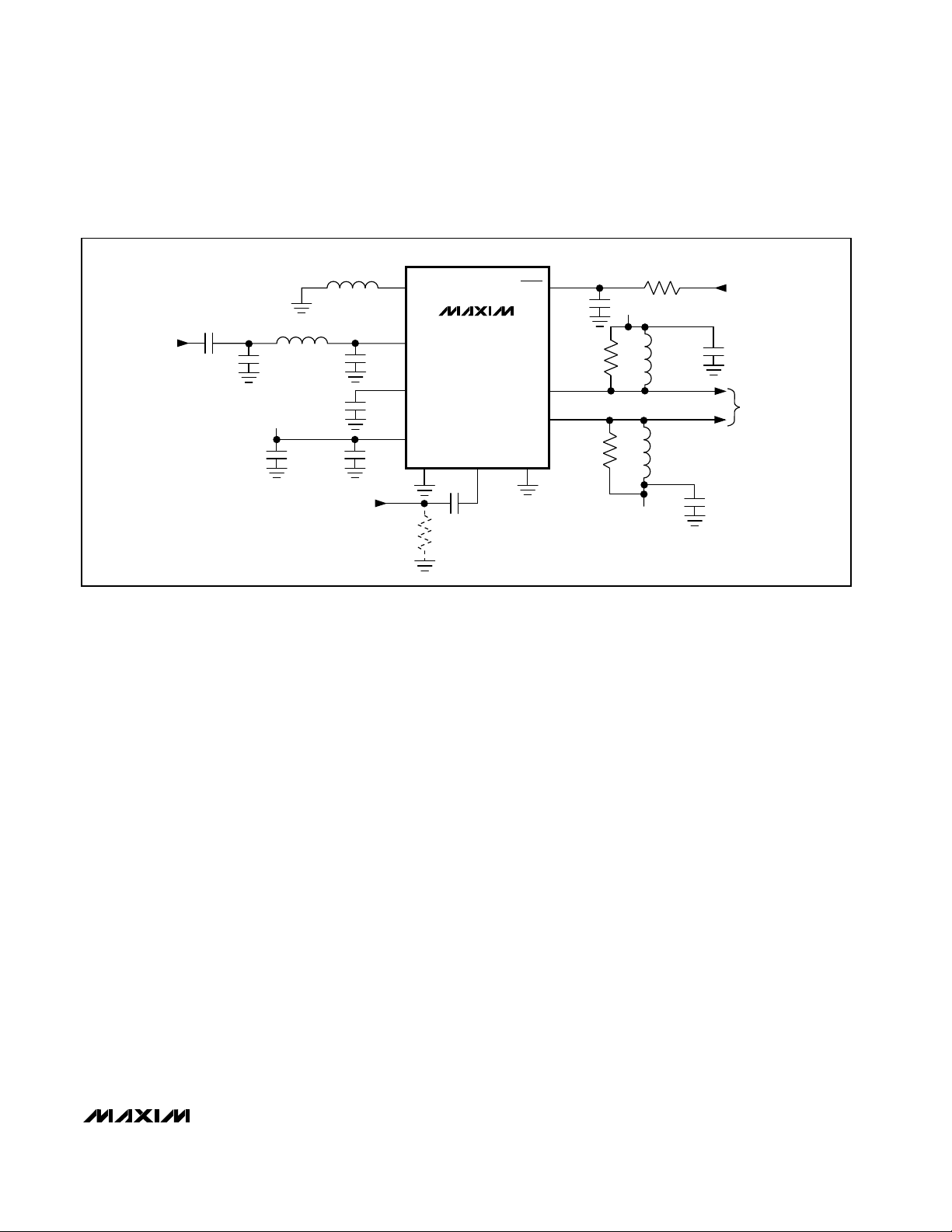
MAX2690
LGND
RFIN
SHDN
1 10
9
8
3
4
5
2
6 7
IFOUT+
IFOUT-
GND LO GNDLO
RFBYP
27nH
3.3nH
1pF
1pF
RF
INPUT
0.5pF
1000pF
1000pF
1000pF
1000pF
IF OUTPUT
TO IF FILTER
IF = 200MHz
SHUTDOWN
CONTROL
1000pF
220nH
220nH
500Ω
500Ω
R
OPTIONAL
(SEE TEXT)
LO
INPUT
0.1pF
1000pF
V
CC
V
CC
100Ω
V
CC
V
CC
RF = 1.95GHz
___________________________________________________Typical Operating Circuit
Page 10

MAX2690
Low-Noise, 2.5GHz
Downconverter Mixer
10 ______________________________________________________________________________________
________________________________________________________Package Information
10LUMAXB.EPS
 Loading...