

Page 1
General Description
The MAX2685’s low-noise amplifier (LNA) and downconverter mixer comprise the major blocks of an RF
front-end receiver. Optimized for 900MHz operation,
the device’s low noise figure, high gain, and high linearity make it ideal for cellular, cordless, and wireless data
applications. A low supply current of 8.5mA (high-gain
mode) and 3.8mA (low-gain mode) plus a low operating
supply voltage range of +2.7V to +5.5V make it suitable
for use in 3-cell NiCd or 1-cell lithium-ion (Li+) battery
applications. A low-power shutdown mode further
extends battery life by reducing supply current below
0.1µA.
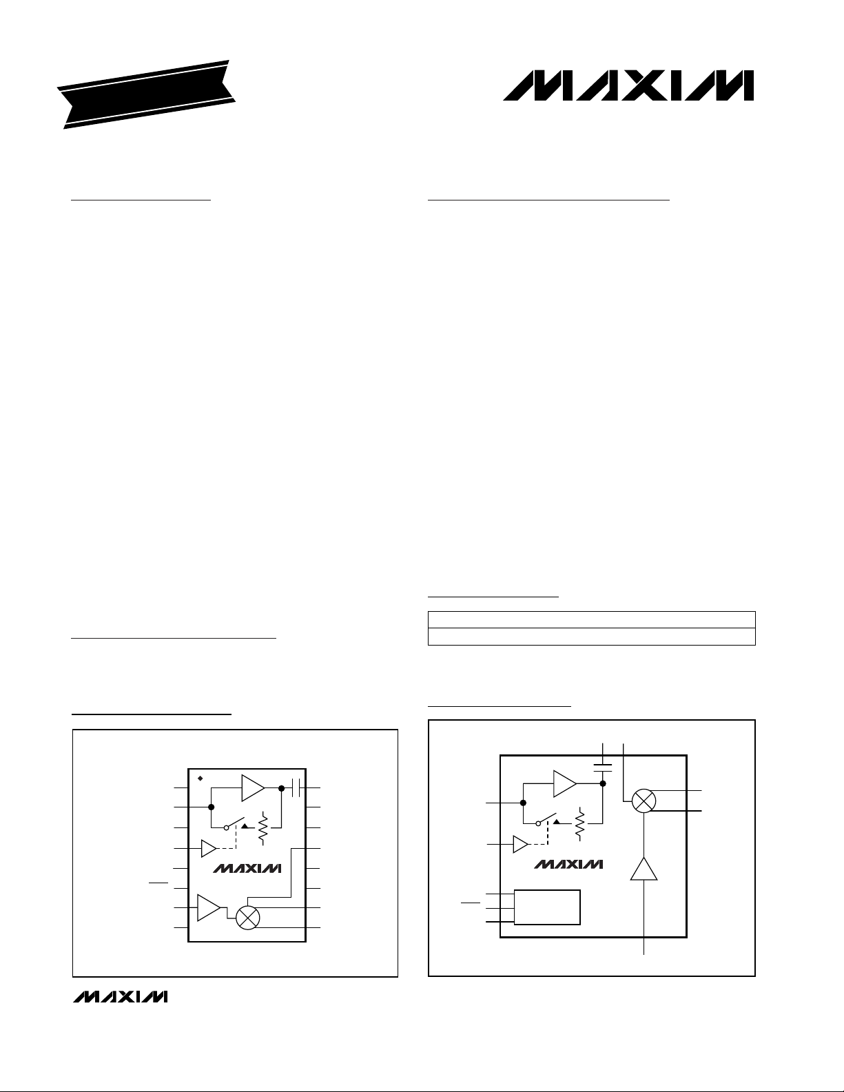
The MAX2685 includes an LNA, LNA bypass switch,
downconverter mixer, and local-oscillator (LO) buffer.
The LNA has a low noise figure of 1.4dB, a high gain of
15dB, and an input third-order intercept point (IP3) of
-4dBm. The mixer has a noise figure of 13dB, a gain of
6dB, and an input IP3 of +7dBm. In addition, an LNA
bypass switch allows two levels of gain, reducing
power consumption when high gain is not needed.
The downconverter mixer has a single-ended RF input
port and differential IF output ports. Differential operation of the IF ports offers improved even-order harmonic
rejection and increased immunity to noise. An LO buffer
allows the LO port to be driven with only -8dBm of LO
power. The MAX2685 is offered in a space-saving 16pin QSOP package.
Applications
Cellular/Cordless Phones 900MHz ISM-Band Radios
Wireless Data 868MHz European ISM Band
Features
♦ 800MHz to 1000MHz RF Frequency Range
♦ +2.7V to +5.5V Single-Supply Operation
♦ Integrated LNA + Mixer + LO Buffer
♦ Logic-Controlled LNA Bypass Switch Reduces
Supply Current
♦ LNA Performance (High/Low Gain)
Gain: +15dB/-12dB
NF: 1.4dB/12dB
Input IP3: -4dBm/+16dBm
♦ Mixer Performance (High/Low Gain)
Gain: 6dB/4.6dB
NF: 13dB/12dB
Input IP3: +7dBm/-1.5dBm
♦ Supply Current
8.5mA (High Gain)
3.8mA (Low Gain)
♦ <0.1µA Supply Current in Shutdown Mode
♦ 0.8µs Receiver Enable Time
MAX2685
Low-Cost, 900MHz, Low-Noise Amplifier
and Downconverter Mixer
________________________________________________________________ Maxim Integrated Products 1
Functional Diagram
19-1493; Rev 1; 12/00
PART
MAX2685EEE -40°C to +85°C
TEMP. RANGE PIN-PACKAGE
16 QSOP
EVALUATION KIT
AVAILABLE
Pin Configuration
Ordering Information
For pricing, delivery, and ordering information, please contact Maxim/Dallas Direct! at
1-888-629-4642, or visit Maxim’s website at www.maxim-ic.com.
MIXIN
LNAOUT
LNA
LNA BYPASS
MAX2685
POWER
MIXER
LO
BUFFER
LO
TOP VIEW
1
GND
2
LNAIN
3
GND
4
GAIN
5
V
CC
6
SHDN
7
LO
8
GND
MAX2685
QSOP
16
15
14
13
12
11
10
9
LNAOUT
V
CC
GND
MIXIN
GND
GND
IFOUT+
IFOUT-
LNAIN
GAIN
V
CC
SHDN
GND
MANAGEMENT
IFOUT+
IFOUT-
Page 2
MAX2685
Low-Cost, 900MHz, Low-Noise Amplifier
and Downconverter Mixer
2 _______________________________________________________________________________________
ABSOLUTE MAXIMUM RATINGS
DC ELECTRICAL CHARACTERISTICS
(VCC= +2.7V to +5.5V, V
SHDN
= +2V, V
GAIN
= +2V, LNAIN = LNAOUT = MIXIN = LO = unconnected, IFOUT+ = IFOUT- = VCC, T
A
= -40°C to +85°C. Typical values are at TA= +25°C and VCC= +3V, unless otherwise noted.)
AC ELECTRICAL CHARACTERISTICS
(MAX2685 EV kit, VCC= V
SHDN
= +3V, f
LNAIN
= f
MIXIN
= 880MHz, fLO= 960MHz, P
LNAIN
= -30dBm, PLO= -8dBm, P
MIXIN
= -25dBm,
differential IFOUT operation, Z
o
= 50Ω, TA= +25°C, unless otherwise noted.)
Stresses beyond those listed under “Absolute Maximum Ratings” may cause permanent damage to the device. These are stress ratings only, and functional
operation of the device at these or any other conditions beyond those indicated in the operational sections of the specifications is not implied. Exposure to
absolute maximum rating conditions for extended periods may affect device reliability.
VCCto GND..............................................................-0.3V to +6V
LNAIN Input Power (50Ω source)...................................+10dBm
LO Input Power (50Ω source) ........................................+10dBm
MIXIN Input Power (50Ω source) ...................................+10dBm
IFOUT+, IFOUT- to GND ..........................................-0.3V to +6V
LNAOUT to GND ......................................................-0.3V to +6V
GAIN, SHDN to GND..................................-0.3V to (V
CC
+ 0.3V)
Continuous Power Dissipation (T
A
= +70°C)
16-Pin QSOP (derate 8.3mW/°C above +70°C)............667mW
Junction Temperature......................................................+150°C
Operating Temperature Range ...........................-40°C to +85°C
Storage Temperature Range .............................-65°C to +150°C
Lead Temperature (soldering, 10s) .................................+300°C
SHDN = GND (Note 1)
GAIN = V
CC
(Note 1)
GAIN, SHDN
GAIN, SHDN
V
SHDN
= V
GAIN
= 0 to 5.5V (Note 1)
CONDITIONS
µA0.1 1.0Shutdown Supply Current
8.5 14.1
V2.7 5.5Supply Voltage Range
V2.0Logic Input Voltage High
V0.5Logic Input Voltage Low
µA±0.01 ±1Logic Input Current
UNITSMIN TYP MAXPARAMETER
GAIN = GND (Note 1)
mA
3.8 6.4
Operating Supply Current
GAIN = GND (Note 1)
dB
-14 -12 -10.3
GAIN = VCC, TA= T
MIN
to T
MAX
(Note 3)
LNA Gain
GAIN = V
CC
(Note 1)
GAIN = V
CC
GAIN = GND
GAIN = V
CC
CONDITIONS
dB0.9 1.6LNA Gain Variation over Temperature
13 15 16.2
1.4
dB
12.2
LNA Noise Figure
-18.4LNA Input 1dB Compression
UNITSMIN TYP MAXPARAMETER
MHz800 1000RF Frequency Range (Note 2)
GAIN = V
CC
GAIN = GND
dBm
-18.6
dB
-11.3
LNAOUT Port Return Loss
MHz800 1000RF Frequency Range (Note 2)
GAIN = GND (Note 1)
dB
2.5 4.6 6.0
Mixer Conversion Gain
GAIN = V
CC
(Note 1) 4.7 6.1 7.0
GAIN = V
CC
(Note 4)
GAIN = GND (Note 5)
-4.1
dBm
+16.2
LNA Input IP3
LOW-NOISE AMPLIFIER (LNA)
DOWNCONVERTER MIXER
Page 3
MAX2685
Low-Cost, 900MHz, Low-Noise Amplifier
and Downconverter Mixer
_______________________________________________________________________________________ 3
AC ELECTRICAL CHARACTERISTICS (continued)
(MAX2685 EV kit, VCC= V
SHDN
= +3V, f
LNAIN
= f
MIXIN
= 880MHz, fLO= 960MHz, P
LNAIN
= -30dBm, PLO= -8dBm, P
MIXIN
= -25dBm,
differential IFOUT operation, Z
o
= 50Ω, TA= +25°C, unless otherwise noted.)
Note 1: Performance at temperatures greater than or equal to +25°C are guaranteed by production test; performance at tempera-
tures less than +25°C are guaranteed by design and characterization.
Note 2: This is the recommended operating frequency range.
Note 3: Maximum and minimum limits are guaranteed by design and device characterization and are not production tested.
Note 4: Two tones at 880MHz and 880.1MHz, -30dBm per tone.
Note 5: Two tones at 880MHz and 880.1MHz, -10dBm per tone.
Note 6: Two tones at 880MHz and 880.1MHz, -25dBm per tone.
Note 7: Time from SHDN = high, until the cascaded receive gain is within 1dB of its final value. Measured with 47pF blocking
capacitors on LNAIN and LNAOUT. Matching network removed from IFOUT output.
Typical Operating Characteristics
(MAX2685 EV kit, VCC= V
SHDN
= +3V, f
LNAIN
= f
MIXIN
= 880MHz, fLO= 960MHz, P
LNAIN
= -30dBm, PLO= -8dBm, P
MIXIN
= -25dBm,
differential IFOUT operation, Z
o
= 50Ω, TA= +25°C, unless otherwise noted.)
0
3
2
1
4
5
6
7
8
9
10
2.5 3.53.0 4.0 4.5 5.0 5.5
SUPPLY CURRENT vs. SUPPLY VOLTAGE
MAX2685 toc01
SUPPLY VOLTAGE (V)
SUPPLY CURRENT (mA)
GAIN = HIGH
GAIN = LOW
TA = +85°C
TA = +25°C
TA = -40°C
TA = +85°C
TA = +25°C
TA = -40°C
0
3
2
1
4
5
6
7
8
9
10
2.5 3.53.0 4.0 4.5 5.0 5.5
SHUTDOWN SUPPLY CURRENT
vs. SUPPLY VOLTAGE
MAX2685 toc02
SUPPLY VOLTAGE (V)
SHUTDOWN SUPPLY CURRENT (nA)
SHDN = GND
TA = -40°C
TA = +25°C
TA = +85°C
-15
-5
-10
5
0
15
10
20
2.5 3.5 4.03.0 4.5 5.0 5.5
LNA GAIN vs. SUPPLY VOLTAGE
MAX2685 toc03
SUPPLY VOLTAGE (V)
GAIN (dB)
GAIN = HIGH
GAIN = LOW
TA = +85°C
TA = +25°C
TA = -40°C
TA = +85°C
TA = +25°C
TA = -40°C
GAIN = GND
dB
12.1
Mixer Noise Figure (SSB)
GAIN = VCC, TA= T
MIN
to T
MAX
(Note 3)
GAIN = V
CC
dB12
Mixer Conversion Gain Variation over
Temperature
(Note 7)
dB
GAIN = V
CC
GAIN = GND
CONDITIONS
µs0.8Receiver Enable Time
13
7
dBm
-1.5
Mixer Input IP3 (Note 6)
11LO Port Return Loss
UNITSMIN TYP MAXPARAMETER
dB
SHDN = VCCor GND
53LO-to-LNAIN Isolation
dB
dB
28LNAOUT-to-MIXIN Isolation
31LO-to-MIXIN Isolation
OVERALL SYSTEM
Page 4

MAX2685
Low-Cost, 900MHz, Low-Noise Amplifier
and Downconverter Mixer
4 _______________________________________________________________________________________
Typical Operating Characteristics (continued)
(MAX2685 EV kit, VCC= V
SHDN
= +3V, f
LNAIN
= f
MIXIN
= 880MHz, fLO= 960MHz, P
LNAIN
= -30dBm, PLO= -8dBm, P
MIXIN
= -25dBm,
differential IFOUT operation, Z
o
= 50Ω, TA= +25°C, unless otherwise noted.)
-10
0
-5
10
5
15
20
2.5 3.5 4.03.0 4.5 5.0 5.5
LNA INPUT IP3 vs. SUPPLY VOLTAGE
MAX2685 toc04
SUPPLY VOLTAGE (V)
INPUT IP3 (dBm)
GAIN = HIGH
GAIN = LOW
TA = +85°C
TA = +25°C
TA = -40°C
TA = +85°C
TA = +25°C
TA = -40°C
-20
-10
-15
0
-5
5
10
15
20
800 850 875825 900 925 950 975 1000
LNA GAIN vs. FREQUENCY
MAX2685 toc05
FREQUENCY (MHz)
GAIN (dB)
GAIN = HIGH
GAIN = LOW
1.0
1.2
1.1
1.4
1.3
1.6
1.5
1.7
1.9
1.8
2.0
870 890 900 910880 920 930 940 950 960
LNA NOISE FIGURE vs. FREQUENCY
MAX2685 toc06
FREQUENCY (MHz)
NOISE FIGURE (dB)
-40
-30
-35
-20
-25
-15
-10
-5
0
800 850 875825 900 925 950 975 1000
LNA REVERSE ISOLATION vs. FREQUENCY
MAX2685 toc07
FREQUENCY (MHz)
REVERSE ISOLATION (dB)
GAIN = HIGH
GAIN = LOW
LNA S11 vs. FREQUENCY
(800MHz to 1000MHz UNMATCHED)
MAX2685 toc10
GAIN = HIGH
GAIN = LOW
800
1000
800
HI
LO
1000
-15
-12
-13
-14
-11
-10
-9
-8
-7
-6
-5
800 880840 920 960 1000
LNA INPUT RETURN LOSS vs. FREQUENCY
MAX2685 toc08
FREQUENCY (MHz)
INPUT RETURN LOSS (dB)
GAIN = HIGH
GAIN = LOW
-20
-14
-16
-18
-12
-10
-8
-6
-4
-2
0
800 880840 920 960 1000
LNA OUTPUT RETURN LOSS vs. FREQUENCY
MAX2685 toc09
FREQUENCY (MHz)
OUTPUT RETURN LOSS (dB)
GAIN = HIGH
GAIN = LOW
3.0
3.5
4.0
4.5
5.0
5.5
6.0
6.5
7.0
2.5 3.53.0 4.0 4.5 5.0 5.5
MIXER GAIN vs. SUPPLY VOLTAGE
MAX2685 toc11
SUPPLY VOLTAGE (V)
GAIN (dB)
TA = -40°C
TA = +85°C
TA = +85°C
TA = +25°C
TA = +25°C
TA = -40°C
GAIN = HIGH
GAIN = LOW
-10
-4
-6
-8
-2
0
2
4
6
8
10
2.5 3.53.0 4.0 4.5 5.0 5.5
MIXER INPUT IP3 vs. SUPPLY VOLTAGE
MAX2685 toc12
SUPPLY VOLTAGE (V)
INPUT IP3 (dBm)
GAIN = HIGH
GAIN = LOW
TA = +85°C
TA = +25°C
TA = -40°C
TA = +85°C
TA = +25°C
TA = -40°C
Page 5

MAX2685
Low-Cost, 900MHz, Low-Noise Amplifier
and Downconverter Mixer
_______________________________________________________________________________________ 5
Typical Operating Characteristics (continued)
(MAX2685 EV kit, VCC= V
SHDN
= +3V, f
LNAIN
= f
MIXIN
= 880MHz, fLO= 960MHz, P
LNAIN
= -30dBm, PLO= -8dBm, P
MIXIN
= -25dBm,
differential IFOUT operation, Z
o
= 50Ω, TA= +25°C, unless otherwise noted.)
-12
-6
-8
-10
-4
-2
0
2
4
6
8
60 70 80 90 100
MIXER GAIN vs. IF FREQUENCY
MAX2685 toc13
IF FREQUENCY (MHz)
GAIN (dB)
BANDWIDTH DETERMINED BY
DIFFERENTIAL-TO-SINGLE-ENDED
CONVERTER CIRCUIT
GAIN = HIGH
GAIN = LOW
0
2
1
4
3
6
5
7
-15 -10 -5 0
MIXER GAIN vs. LO POWER
MAX2685 toc14
LO POWER (dBm)
GAIN (dB)
GAIN = HIGH
GAIN = LOW
10.0
11.5
11.0
10.5
12.0
12.5
13.0
13.5
14.0
14.5
15.0
-15 -10 -5 0
MIXER NOISE FIGURE vs. LO POWER
MAX2685 toc15
LO POWER (dBm)
NOISE FIGURE (dB)
GAIN = HIGH
GAIN = LOW
-15
-12
-13
-14
-10
-11
-6
-7
-8
-9
-5
750 800 850 900 950 1000 1050 1100
LO PORT RETURN LOSS vs. FREQUENCY
MAX2685 toc16
FREQUENCY (MHz)
RETURN LOSS (dB)
Page 6

MAX2685
Low-Cost, 900MHz, Low-Noise Amplifier
and Downconverter Mixer
6 _______________________________________________________________________________________
Pin Description
NAME FUNCTION
1, 3, 8,
11, 12, 14
GND Ground. Connect to ground plane with a low-inductance connection.
2 LNAIN
RF Input to LNA and LNA Bypass Switch. Requires an external matching network and a series
DC-blocking capacitor.
PIN
4 GAIN
Gain Control Logic-Level Input. Drive high to enable the LNA, open the LNA bypass switch, and
increase the receiver’s gain. Drive low to disable the LNA, close the LNA bypass switch, and reduce
the receiver’s gain.
5, 15 V
CC
Supply Voltage. Bypass VCCto GND at each pin with a 47pF capacitor as close to the pin as possible.
6
SHDN
Shutdown Control Logic-Level Input. Drive high or connect to VCCfor normal operation. Drive low to
place the device in low-power shutdown mode.
7 LO
Local-Oscillator Input to Downconverter Mixer. Requires a series DC-blocking capacitor and an impedance-setting resistor (typically 75Ω to ground).
9 IFOUT-
Inverting Side to Downconverter Mixer’s Differential Open-Collector IF Output. Requires a pull-up inductor to VCCfor proper biasing, as well as a matching network to ensure optimum output power.
10 IFOUT+
Noninverting Side of Downconverter Mixer’s Differential Open-Collector IF Output. Requires a pull-up
inductor to VCCfor proper biasing, as well as a matching network to ensure optimum output power.
13 MIXIN
RF Input to Downconverter Mixer. Requires an external matching network and series DC-blocking
capacitor.
16 LNAOUT LNA Output. Internally matched to 50Ω. LNAOUT has an internal blocking capacitor.
Figure 1. Typical Operating Circuit
LNA
INPUT
880MHz
SHUTDOWN
LO
INPUT
960MHz
3.3pF
680nH
47pF
300pF
V
CC
6pF
300pF
6pF
820nH
12pF
LNA
OUTPUT
MIXER
INPUT
880MHz
IF
OUTPUT
80MHz
V
CC
1000pF
GAIN-
CONTROL
INPUT
INPUT
0.1µF
1
GND LNAOUT
12nH
V
CC
47pF
330pF
75Ω
2
3
4
5
6
7
8
LNAIN
GND
GAIN
V
CC
SHDN
LO
GND
MAX2685
V
GND
MIXIN
GND
GND
IFOUT+
IFOUT-
16
15
CC
14
13
12
11
10
R*
9
*OPTIONAL FOR BROADBAND MATCH.
Page 7

Detailed Description
The MAX2685 consists of five major components: a
low-noise amplifier (LNA), an LNA bypass switch, a
downconverter mixer, a local-oscillator (LO) buffer, and
a power-management block.
Low-Noise Amplifier (LNA)
The LNA is a wideband, single-ended cascode amplifier that operates over a wide range of frequencies. The
input of the LNA (LNAIN) requires an appropriate
matching network and a DC-blocking capacitor. The
typical operating circuit shown in Figure 1 is optimized
for frequencies around 880MHz, requiring only a 0.1µF
capacitor in series with a 12nH inductor. See Table 1
for the LNA “S” parameters for matching to other frequencies.
The output of the LNA (LNAOUT) is internally biased to
VCC. It is internally matched to 50Ω and incorporates
an internal DC-blocking capacitor.
LNA Bypass Switch
and Gain Control
When a large input signal is present, enable the LNA
bypass function to increase linearity and reduce supply
current. Set GAIN low to enable the LNA bypass function.
Receive Mixer
The downconverter mixer is a wideband, single-balanced design with a low noise figure and high linearity.
The RF signal at the MIXIN port is mixed with the signal
at the LO port, and is downconverted to an IF frequency at the differential IF port.
RF Input
The MIXIN input requires a simple external matching
network and a series DC-blocking capacitor. See
Figure 1 for a matching network example, optimized for
880MHz operation. Table 2 lists mixer “S” parameters
for matching to other frequencies.
MAX2685
Low-Cost, 900MHz, Low-Noise Amplifier
and Downconverter Mixer
_______________________________________________________________________________________ 7
Table 1. LNA Typical S-Parameters (VCC= +3V, TA= +25°C)
|
S11
|
MAG
FREQUENCY
(MHz)
800 0.761
S11
PHASE
(degrees)
-64.5
|
S21
|
MAG
S21
PHASE
(degrees)
177.94.98
|
S12
|
MAG
S12
PHASE
(degrees)
-163.7
|
S22
|
MAG
S22
PHASE
(degrees)
-107.30.3760.018
-68.6 167.25.06 -167.1840 0.753 -107.00.2640.022
-73.2 156.65.07 -171.3880 0.747 -94.60.1720.026
-78.0 146.64.91 -175.7920 0.733 -62.90.1490.030
-82.8 137.74.68 178.0960 0.719 -42.40.2000.035
-87.5 130.34.40 171.01000 0.693 -38.80.2630.039
-45.6 73.00.188 71.9800 0.625 -91.30.4830.191
-48.1 65.50.195 64.2840 0.621 -91.30.4230.198
-50.9 58.10.199 56.7880 0.619 -89.90.3700.201
-53.3 51.60.200 50.3920 0.611 -86.10.3370.202
-55.5 46.10.200 44.7960 0.608 -80.90.3220.201
-57.5 41.20.200 40.01000 0.607 -76.70.3170.200
High-Gain Mode (GAIN = VCC)
Low-Gain Mode (GAIN = GND)
Page 8

MAX2685
Low-Cost, 900MHz, Low-Noise Amplifier
and Downconverter Mixer
8 _______________________________________________________________________________________
Table 2. Mixer Typical S-Parameters (VCC= +3V, TA= +25°C)
S11
MAG
|
S11
|
PHASE
(degrees)
152.7
|
S22
|
MAG (IFOUT+
Port Only)
S22 PHASE
(IFOUT+ Port
Only)
(degrees)
-0.4
IF FREQUENCY
(MHz)
10
RF FREQUENCY
(MHz)
0.996
-1.840
800 0.355
0.994
-3.280 0.993
153.7
-4.2110 0.989
840 0.352
-6.2170 0.988
154.5
-8.0240 0.983
880 0.351
155.8920 0.349
156.2960 0.352
156.91000 0.353
142.8 -0.510 0.996
-1.840
800 0.275
0.995
-3.280 0.993
144.1
-4.2110 0.989
840 0.268
-6.2170 0.987
145.5
-7.9240 0.982
880 0.262
147.7920 0.255
149.0960 0.254
156.91000 0.245
High-Gain Mode (GAIN = VCC)
Low-Gain Mode (GAIN = GND)
Page 9

MAX2685
Low-Cost, 900MHz, Low-Noise Amplifier
and Downconverter Mixer
_______________________________________________________________________________________ 9
Local-Oscillator Input
The LO port is the high-impedance input of the localoscillator buffer. It requires a series DC-blocking
capacitor and a shunt resistor to ground to set the input
impedance. See the Typical Operating Characteristics
for a graph of LO Port Return Loss vs. Frequency.
IF Output Port
The mixer’s downconverted output appears on the differential IFOUT+ and IFOUT- pins. The differential output can be converted to a single-ended output, as
shown in the MAX2685 evaluation kit (EV kit). Refer to
the Detailed Description in the MAX2685 EV kit data
sheet.
Shutdown
Drive SHDN low to disable all device functions and
place the MAX2685 in low-power shutdown mode.
Drive SHDN high or connect it to VCCto enable all
device functions.
Applications Information
Layout Considerations
A properly designed PC board is an essential part of
any RF/microwave circuit. Note the IC’s high-frequency
inputs and outputs, and be sure to decouple the DC
supply and control pins.
For power-supply traces and connections, a star topology works well. Each VCCnode in the circuit has its
own path to the central VCCnode and a decoupling
capacitor that provides a low impedance at the RF frequency of interest. The central VCCalso has a large
decoupling capacitor. This provides good isolation
between the different sections of the MAX2685.
Chip Information
TRANSISTOR COUNT: 295
Page 10

MAX2685
Low-Cost, 900MHz, Low-Noise Amplifier
and Downconverter Mixer
Package Information
Maxim cannot assume responsibility for use of any circuitry other than circuitry entirely embodied in a Maxim product. No circuit patent licenses are
implied. Maxim reserves the right to change the circuitry and specifications without notice at any time.
10 ____________________Maxim Integrated Products, 120 San Gabriel Drive, Sunnyvale, CA 94086 408-737-7600
© 2000 Maxim Integrated Products Printed USA is a registered trademark of Maxim Integrated Products.
QSOP.EPS
 Loading...