Page 1

E V A L U A T I O N K IT A V A I L A B L E
19-5655; Rev 0; 6/11
MAX2670
GPS/GNSS Front-End Amplifier
General Description
The MAX2670 GPS/GNSS front-end amplifier IC is
designed for automotive and marine GPS/GNSS satellite
navigation antenna modules or for any application that
needs to compensate for cable losses from the antenna
to receiver. Two unconditionally stable low-noise amplifier
stages provide the high gain and integrated I/O matching
to minimize the need for external matching components
and eliminate the need for additional gain stages. The
device features the option to place a bandpass ceramic
or SAW filter between the two amplifier stages to provide
a narrow-band output to further improve the noise performance of the GPS/GNSS receiver. Additionally, a 3.4dB
gain step is provided to compensate for cable loss variation between different applications.
The device is designed to operate across all GNSS frequency standards with a 34.8dB typical cascaded gain
and a 25mA supply current. The two LNA stages allow
the use of a wide range of GNSS filter types for maximum flexibility in system design. The final RF output pin,
which drives the cable to the GNSS receiver, is also the
power-supply connection that accepts a DC supply in
the 3.0V to 5.5V range. Alternatively, the DC supply can
be applied to pin 4.
This GPS/GNSS front-end amplifier is designed on a lownoise, advanced SiGe process and is available in a leadfree, 10-pin TDFN surface-mount package (3mm x 3mm).
Features
S First Amplifier Noise Figure*: 1.0dB
S High Gain**: 34.8dB
S 3.4dB Gain Step
S Shared V
and RFOUT2 Pin
CC
S Integrated 50I Output Matching
S 3.0V to 5.5V Supply Voltage Range
S Small, Low-Cost Package (3mm x 3mm)
S AEC-Q100 Qualified
S ESD Protected to ±2kV Human Body Model
Applications
Integrated Automotive and Marine GPS Receivers
Active Antennas
*Without external input impedance match.
**First amplifier input is impedance matched (S11 = -10dB).
Second amplifier set to high gain. Amplifiers cascaded without
interstage filter.
Ordering Information appears at end of data sheet.
Typical Operating Circuit appears at end of data sheet.
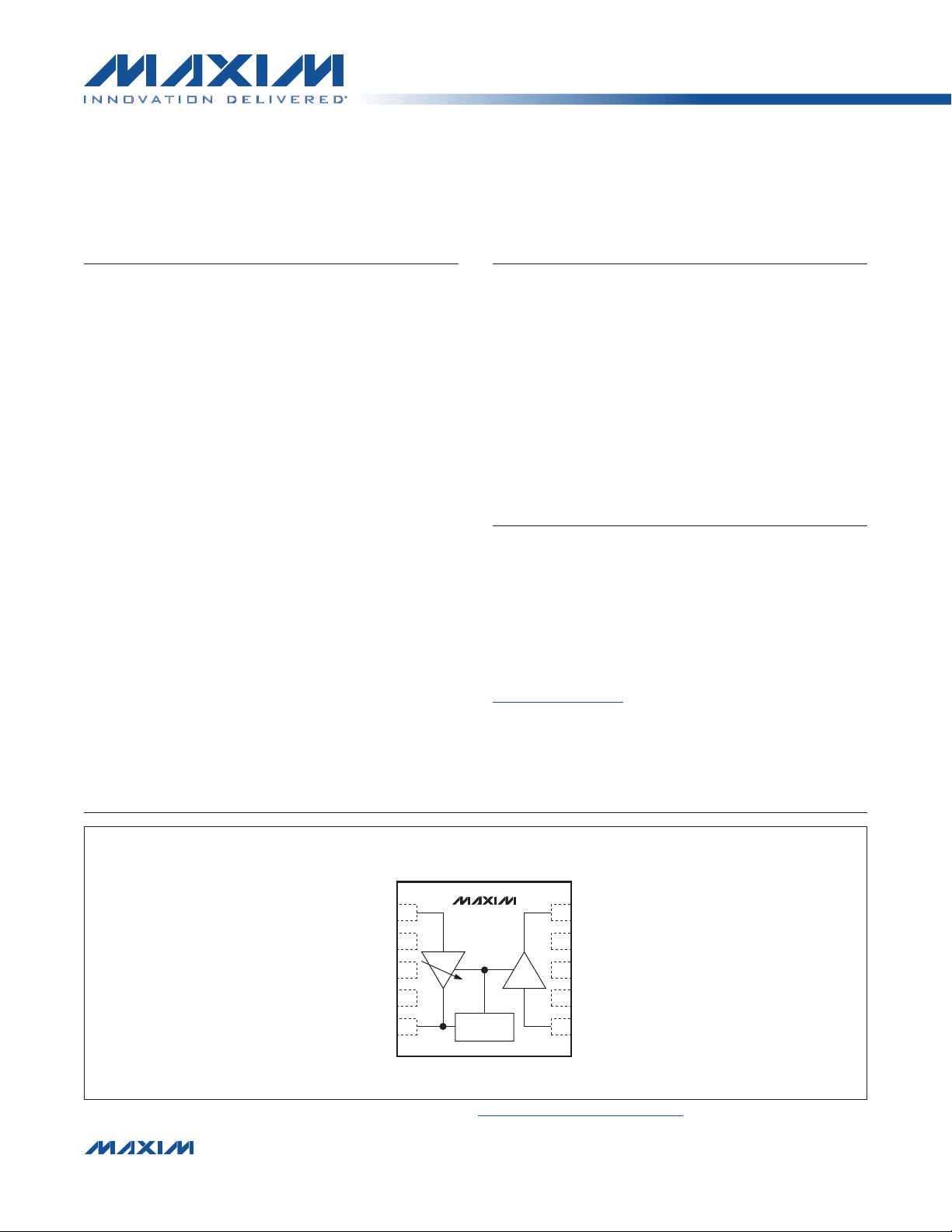
Functional Diagram
TOP VIEW
+
RFIN2
1
2 9
GND
3
EXTCAP/ALT_VCC
For related parts and recommended products to use with this part, refer to www.maxim-ic.com/MAX2670.related.
����������������������������������������������������������������� Maxim Integrated Products 1
4
5 6
MAX2670
AMP 2
AMP 1
DC
GENERATION
TDFN
For pricing, delivery, and ordering information, please contact Maxim Direct at 1-888-629-4642,
or visit Maxim’s website at www.maxim-ic.com.
RFOUT1
10
GNDGND
GND
8
GAIN_SELECT
7
RFIN1RFOUT2/VCC
Page 2

MAX2670
GPS/GNSS Front-End Amplifier
ABSOLUTE MAXIMUM RATINGS
RFOUT1, RFOUT2, EXTCAP to GND ....... -0.3V to (VCC + 0.5V)
RFIN1 Input Power (50I source) .................................. +15dBm
GAIN_SELECT to GND ............................. -0.3V to (VCC + 0.3V)
Continuous Power Dissipation (TA = +70NC)
TDFN (derate 18.5mW/NC above +70NC) ..................1481mW
Operating Ambient Temperature Range .........-40NC to +105NC
Maximum Junction Temperature .....................................+150NC
Stresses beyond those listed under “Absolute Maximum Ratings” may cause permanent damage to the device. These are stress ratings only, and functional operation of the device at these or any other conditions beyond those indicated in the operational sections of the specifications is not implied. Exposure to absolute
maximum rating conditions for extended periods may affect device reliability.
DC ELECTRICAL CHARACTERISTICS
(VIN = 3.0V to 5.5V, TA = -40NC to +105NC. Typical values are at +5.0V and at TA = +25NC. Pin 7 open, unless otherwise noted.)
(Note 1)
PARAMETER SYMBOL CONDITIONS MIN TYP MAX UNITS
Supply Voltage V
Supply Current I
Gain-Select Input Current I
CC
CC
3.0 5.5 V
TA = +25NC
TA = -40NC to 105NC
VIL = 0V 20 100
IL
Storage Temperature Range ............................ -65NC to +150NC
Lead Temperature (soldering, 10s) ................................+300NC
Soldering Temperature (reflow) ......................................+260NC
15.0 25 30
30
mA
FA
AC ELECTRICAL CHARACTERISTICS
(VCC = 3.0V to 5.5V, PIN = -40dBm, fIN = 1575MHz, TA = -40NC to +105NC. Typical values are at 5.0V and at TA = +25NC. Input
matched to 50I, load = 50I, pin 7 open, unless otherwise noted.) (Note 1)
PARAMETER SYMBOL CONDITIONS MIN TYP MAX UNITS
Operation Frequency f
AMP 1 Gain
AMP 1 Gain Variation Over
Temperature
AMP 1 Noise Figure NF No input match (Notes 2, 3) 1 dB
AMP 1 Input Third-Order
Intercept Point
AMP 1 Input 1dB Compression
Point
AMP 1 Input Return Loss
AMP 1 Output Return Loss
AMP 1 Reverse Isolation
AMP 2 Gain
AMP 2 Gain Step Gain change when pin 7 is shorted to GND -2.5 -3.4 -4.0 dB
AMP 2 Gain Variation Over
Temperature
AMP 2 Noise Figure NF (Note 3) 2.0 dB
RF
|S21|
IIP3
|S11|
|S22|
|S12|
|S21|
50I source with no input match (Note 2)
50I source with input match
Two tones at 1574.5MHz and 1575.5MHz,
-35dBm per tone
50I source with no input match (Note 2)
No input match (Note 2) -4.4 dB
14.5 16.7 19
14.5 17 21 dB
1575 MHz
17.8
0.3 dB
-12 dBm
-19 dBm
-14.5 dB
-33 dB
1 dB
dB
����������������������������������������������������������������� Maxim Integrated Products 2
Page 3

MAX2670
(WITHOUT EXTERNAL INPUT IMPEDANCE MATCH)
NOISE FIGURE (dB)
GPS/GNSS Front-End Amplifier
AC ELECTRICAL CHARACTERISTICS (continued)
(VCC = 3.0V to 5.5V, PIN = -40dBm, fIN = 1575MHz, TA = -40NC to +105NC. Typical values are at 5.0V and at TA = +25NC. Input
matched to 50I, load = 50I, pin 7 open, unless otherwise noted.) (Note 1)
PARAMETER SYMBOL CONDITIONS MIN TYP MAX UNITS
AMP 2 Output Third-Order
Intercept Point
OIP3
AMP 2 Output 1dB Compression
Point
AMP 2 Input Return Loss
AMP 2 Output Return Loss
AMP 2 Reverse Isolation
|S11|
|S22|
|S12|
Note 1: TA = +25NC and TA = +105NC are guaranteed by production test. At TA = -40NC, the minimum and maximum values are
guaranteed by design and characterization, unless otherwise noted.
Note 2: Measured using the MAX2670 evaluation board with a DC-blocking capacitor at the input of LNA 1.
Note 3: At TA = +25NC, the maximum value is guaranteed by design and characterization. Specification is corrected for board
losses on the MAX2670 EV kit.
Two tones at 1574.5MHz and 1575.5MHz,
-30dBm per tone
16.0 dBm
5.3 dBm
-21 dB
-8.8 dB
-25 dB
(PIN = -40dBm, fIN = 1575MHz, inputs and outputs are terminated to 50I, VCC = 5.0V, TA = +25NC, unless otherwise noted.)
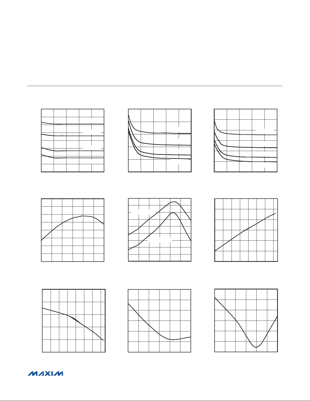
AMP 1 NOISE FIGURE vs. TEMPERATURE
1.4
1.3
1.2
1.1
1.0
0.9
0.8
0.7
0.6
-40 0 20-20 40 60 80 100
TEMPERATURE (°C)
MAX2670 toc01
Typical Operating Characteristics
AMP 2 NOISE FIGURE vs. TEMPERATURE
5.5
5.0
4.5
4.0
3.5
3.0
NOISE FIGURE (dB)
2.5
2.0
1.5
1.0
-40 0 20-20 40 60 80 100
TEMPERATURE (°C)
LOW-GAIN MODE
HIGH-GAIN MODE
27.5
MAX2670 toc02
26.5
25.5
24.5
23.5
SUPPLY CURRENT (mA)
22.5
21.5
SUPPLY VOLTAGE vs. CURRENT
(PIN 7 OPEN)
TA = +105°C
MAX2670 toc03
TA = +85°C
TA = +25°C
TA = -40°C
3.0 4.03.5 4.5 5.0 5.5
SUPPLY VOLTAGE (V)
����������������������������������������������������������������� Maxim Integrated Products 3
Page 4

MAX2670
(WITHOUT EXTERNAL INPUT IMPEDANCE MATCH)
GPS/GNSS Front-End Amplifier
Typical Operating Characteristics (continued)
(PIN = -40dBm, fIN = 1575MHz, inputs and outputs are terminated to 50I, VCC = 5.0V, TA = +25NC, unless otherwise noted.)
AMP 1 GAIN vs. SUPPLY VOLTAGE
(WITH EXTERNAL INPUT IMPEDANCE MATCH)
18.1
18.0
17.9
17.8
17.7
GAIN (dB)
17.6
17.5
17.4
17.3
3.0 4.03.5 4.5 5.0 5.5
SUPPLY VOLTAGE (V)
TA = -40°C
TA = +25°C
TA = +85°C
TA = +105°C
AMP 1 GAIN vs. FREQUENCY
(WITH EXTERNAL INPUT IMPEDANCE MATCH)
20
19
18
17
16
GAIN (dB)
15
14
13
12
800 12001000 1400 1600 1800 2000
FREQUENCY (MHz)
MAX2670 toc04
MAX2670 toc07
AMP 2 GAIN vs. SUPPLY VOLTAGE
(PIN 7 OPEN)
18.0
17.5
17.0
GAIN (dB)
16.5
16.0
15.5
3.0 4.03.5 4.5 5.0 5.5
SUPPLY VOLTAGE (V)
TA = -40°C
TA = +25°C
TA = +85°C
TA = +105°C
AMP 2 GAIN vs. FREQUENCY
18
16
HIGH-GAIN MODE
14
12
10
8
GAIN (dB)
6
4
2
0
800 12001000 1400 1600 1800 2000
LOW-GAIN MODE
FREQUENCY (MHz)
AMP 2 GAIN vs. SUPPLY VOLTAGE
(PIN 7 SHORT TO GND)
15.0
14.5
MAX2670 toc05
14.0
13.5
GAIN (dB)
13.0
12.5
12.0
3.0 4.03.5 4.5 5.0 5.5
SUPPLY VOLTAGE (V)
AMP 1 INPUT P
vs. TEMPERATURE
1dB
(WITHOUT EXTERNAL INPUT IMPEDANCE MATCH)
-16
-17
MAX2670 toc08
-18
(dBm)
1dB
-19
INPUT P
-20
-21
-22
-40 0 20-20 40 60 80 100
TEMPERATURE (°C)
TA = -40°C
TA = +25°C
TA = +85°C
TA = +105°C
MAX2670 toc06
MAX2670 toc09
AMP 2 OUTPUT P
vs. TEMPERATURE
1dB
(PIN 7 OPEN)
5.8
5.6
(dB)
5.4
1dB
5.2
OUTPUT P
5.0
4.8
-40 0 20-20 40 60 80 100
TEMPERATURE (°C)
����������������������������������������������������������������� Maxim Integrated Products 4
MAX2670 toc10
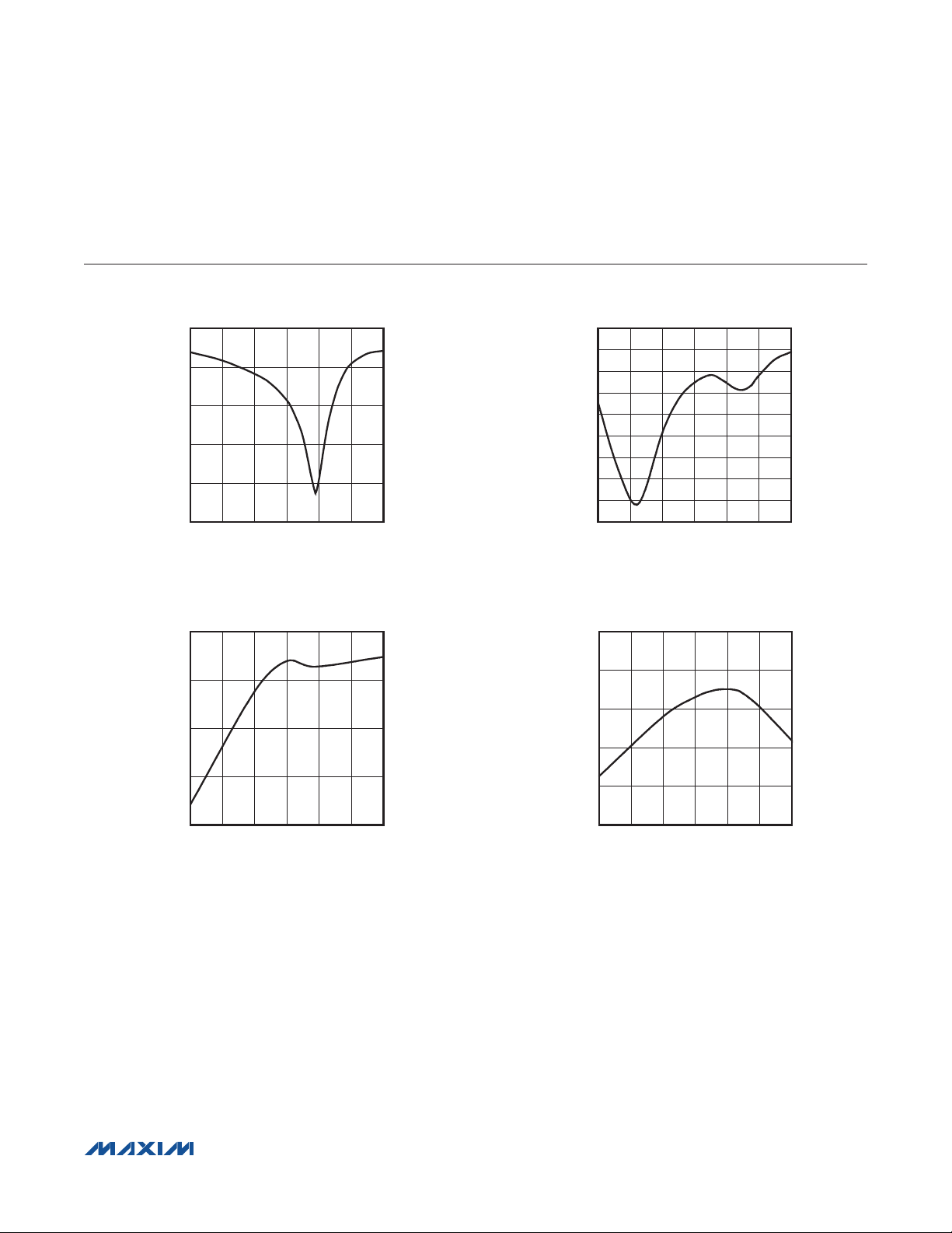
AMP 1 S11
-2.0
-2.5
-3.0
-3.5
S11 (dB)
-4.0
-4.5
-5.0
800 12001000 1400 1600 1800 2000
FREQUENCY (MHz)
MAX2670 toc11
AMP 1 S22
-4
-6
-8
-10
S22 (dB)
-12
-14
-16
800 12001000 1400 1600 1800 2000
FREQUENCY (MHz)
MAX2670 toc12
Page 5

MAX2670
GPS/GNSS Front-End Amplifier
Typical Operating Characteristics (continued)
(PIN = -40dBm, fIN = 1575MHz, inputs and outputs are terminated to 50I, VCC = 5.0V, TA = +25NC, unless otherwise noted.)
AMP 2 S11
0
-5
-10
S11 (dB)
-15
-20
-25
800 12001000 1400 1600 1800 2000
FREQUENCY (MHz)
AMP 1 S12
-32
-34
-36
S12 (dB)
MAX2670 toc13
MAX2670 toc15
AMP 2 S22
-4
-6
-8
-10
-12
-14
S22 (dB)
-16
-18
-20
-22
800 12001000 1400 1600 1800 2000
FREQUENCY (MHz)
AMP 2 S12
-20
-24
-28
S12 (dB)
-32
MAX2670 toc14
MAX2670 toc16
-38
-40
800 12001000 1400 1600 1800 2000
FREQUENCY (MHz)
-36
-40
800 12001000 1400 1600 1800 2000
FREQUENCY (MHz)
����������������������������������������������������������������� Maxim Integrated Products 5
Page 6

TOP VIEW
MAX2670
GPS/GNSS Front-End Amplifier
Pin Configuration
+
RFIN2
1
RFOUT1
10
GNDGND
GND
8
GAIN_SELECT
7
RFIN1RFOUT2/VCC
GND
EXTCAP/ALT_VCC
2 9
3
4
5 6
MAX2670
EP
TDFN
Pin Description
PIN NAME FUNCTION
1 RFIN2
2, 3, 8, 9 GND Electrical Ground
4 EXTCAP/ALT_VCC
5 RFOUT2/VCC
6 RFIN1 Amplifier 1 Input. Requires external DC-blocking capacitor and matching components.
7 GAIN_SELECT AMP 2 Gain Select. Open is high-gain mode. Short to ground is low-gain mode.
10 RFOUT1
EP —
Amplifier 2 Input. Incorporates an internal DC-blocking capacitor and is internally matched to
50I. This input is designed to be connected to a bandpass filter.
External Smoothing Capacitor for Internal Supply Voltage or Can Be Used as the External DC
Supply Pin to Eliminate the Need for a Bias-T on RFOUT2/VCC.
Amplifier 2 Output. Incorporates an internal DC-blocking capacitor and is internally matched to
50I. DC bias on this pin serves as the power supply through a bias-T.
Amplifier 1 Output. Incorporates an internal DC-blocking capacitor and is internally matched to
50I. This output is designed to drive a bandpass filter.
Exposed Pad Ground. The exposed pad must be soldered to the circuit board for proper thermal
and electrical performance.
����������������������������������������������������������������� Maxim Integrated Products 6
Page 7

MAX2670
GPS/GNSS Front-End Amplifier
Detailed Description
The MAX2670 IC contains two LNA stages tuned for use
at 1575MHz.
AMP 1
AMP 1 has an internal load that limits the bandwidth and
provides a 50I output impedance through a DC-blocking
capacitor. The internal biasing for AMP 1 suppresses
gain variation with changes in temperature and supply
voltage. At the input, an integrated DC-blocking capacitor and matching network are intentionally omitted to
allow selection of external components to optimize for
noise or gain.
AMP 2 with Gain Step
The output of AMP 2 has the dual role of providing both
the RF output drive and receiving the DC power supply
through a single cable. Both the input and output ports
of AMP 2 are internally matched to 50I impedance at
1575MHz. A 3.4dB gain switch can be used to adjust
the gain for different applications. The gain-select pin is
connected to an inverter with an internal pullup resistor.
Hence, the gain-select pin is set by default to high-gain
mode. Shorting the gain-select pin to ground sets the
gain stage to a 3.4dB lower gain. As with AMP 1, AMP
2 has an internal load that limits the bandwidth, and the
amplifier’s internal biasing suppresses gain variation with
changes in temperature and supply voltage.
Alternate Supply (ALT_VCC)
The IC power can be supplied from the navigation system through RFOUT2 (pin 5). An integrated filter is connected to the output of LNA 2 to separate the supply voltage from the GPS signal. Alternatively, the supply voltage
can be applied to the external capacitor pin (pin 4).
Layout Considerations
For best performance, carefully lay out the PCB using
high-frequency techniques. Use controlled-impedance
transmission lines to interface with the MAX2670 highspeed inputs and outputs and isolate the input signals from the output signals as much as possible. For
improved noise figure, keep the connection to the input
of LNA 1 as short as possible. A power-supply decoupling capacitor should be placed very close to pin 4 and
connected directly to a ground plane. If low-gain selection for LNA 2 is required, connect pin 7 directly to the
ground plane with a very short PCB trace. Good grounding is critical for this device. The backside ground plane
should be as close as possible.
Refer to www.maxim-ic.com for the MAX2670 Evaluation
Kit schematic, gerber data, pads layout file and BOM
information.
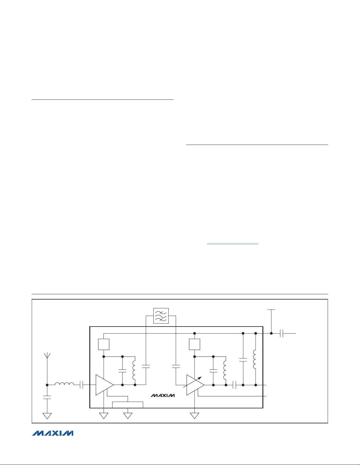
Typical Operating Circuit
SAW
LNA2 INPUTLNA1 INPUT
10
V
CC
REG
6
LNA 1
EXPOSED PAD
8/9
����������������������������������������������������������������� Maxim Integrated Products 7
MAX2670
1
V
CC
REG
LNA 2
2/3
ALT_VCC
4
5
RFOUT2/VCC
GAIN_SELECT
7
OPEN = 31.4dB GAIN
SHORT TO GROUND = 28dB GAIN
Page 8

MAX2670
GPS/GNSS Front-End Amplifier
Ordering Information
PART TEMP RANGE PIN-PACKAGE
MAX2670GTB+T
MAX2670GTB/V+T
+Denotes a lead(Pb)-free/RoHS-compliant package.
T = Tape and reel.
*EP = Exposed pad.
/V denotes automotive qualified part.
-40NC to +105NC
-40NC to +105NC
10 TDFN-EP*
10 TDFN-EP*
Package Information
For the latest package outline information and land patterns
(footprints), go to www.maxim-ic.com/packages. Note that a
“+”, “#”, or “-” in the package code indicates RoHS status only.
Package drawings may show a different suffix character, but
the drawing pertains to the package regardless of RoHS status.
PACKAGE
TYPE
10 TDFN-EP T1033+2
PACKAGE
CODE
OUTLINE
NO.
21-0137 90-0061
LAND
PATTERN NO.
����������������������������������������������������������������� Maxim Integrated Products 8
Page 9

MAX2670
GPS/GNSS Front-End Amplifier
Revision History
REVISION
NUMBER
0 6/11 Initial release —
REVISION
DATE
DESCRIPTION
PAGES
CHANGED
Maxim cannot assume responsibility for use of any circuitry other than circuitry entirely embodied in a Maxim product. No circuit patent licenses are implied.
Maxim reserves the right to change the circuitry and specifications without notice at any time. The parametric values (min and max limits) shown in the Electrical
Characteristics table are guaranteed. Other parametric values quoted in this data sheet are provided for guidance.
Maxim Integrated Products, 120 San Gabriel Drive, Sunnyvale, CA 94086 408-737-7600 9
©
2011 Maxim Integrated Products Maxim is a registered trademark of Maxim Integrated Products, Inc.
 Loading...