

Page 1
General Description
The MAX2659 high-gain, low-noise amplifier (LNA) is
designed for GPS, Galileo, and GLONASS applications.
Designed in Maxim’s advanced SiGe process, the
device achieves a 20.5dB gain and an ultra-low-noise
figure of 0.8dB while maximizing the input-referred 1dB
compression point and the 3rd-order intercept point at 12dBm and -5dBm, respectively.
The MAX2659 operates from a +1.6V to +3.3V single
supply and consumes only 4.1mA. The shutdown feature in the device reduces the supply current to be less
than 1µA. The MAX2659 is available in a very small,
lead-free, RoHS-compliant, 1.5mm x 1.0mm x 0.75mm,
6-pin µDFN package.
.
Applications
Automotive Navigation
Location-Enabled Mobile Devices
Telematics (Asset Tracking and Management)
Personal Navigation Device (PND)
Cellular Phones with GPS
Notebook PC/Ultra-Mobile PC
Recreational, Marine Navigation
Avionics
Features
o High-Power Gain: 20.5dB
o Ultra-Low-Noise Figure: 0.8dB
o Integrated 50Ω Output Matching Circuit
o Low Supply Current: 4.1mA
o Wide Supply Voltage Range: 1.6V to 3.3V
o Low Bill of Materials
o Small Footprint: 1.5mm x 1.0mm
o Thin Profile: 0.75mm
o Lead-Free and RoHS-Compliant Package
MAX2659
GPS/GNSS Low-Noise Amplifier
________________________________________________________________
Maxim Integrated Products
1
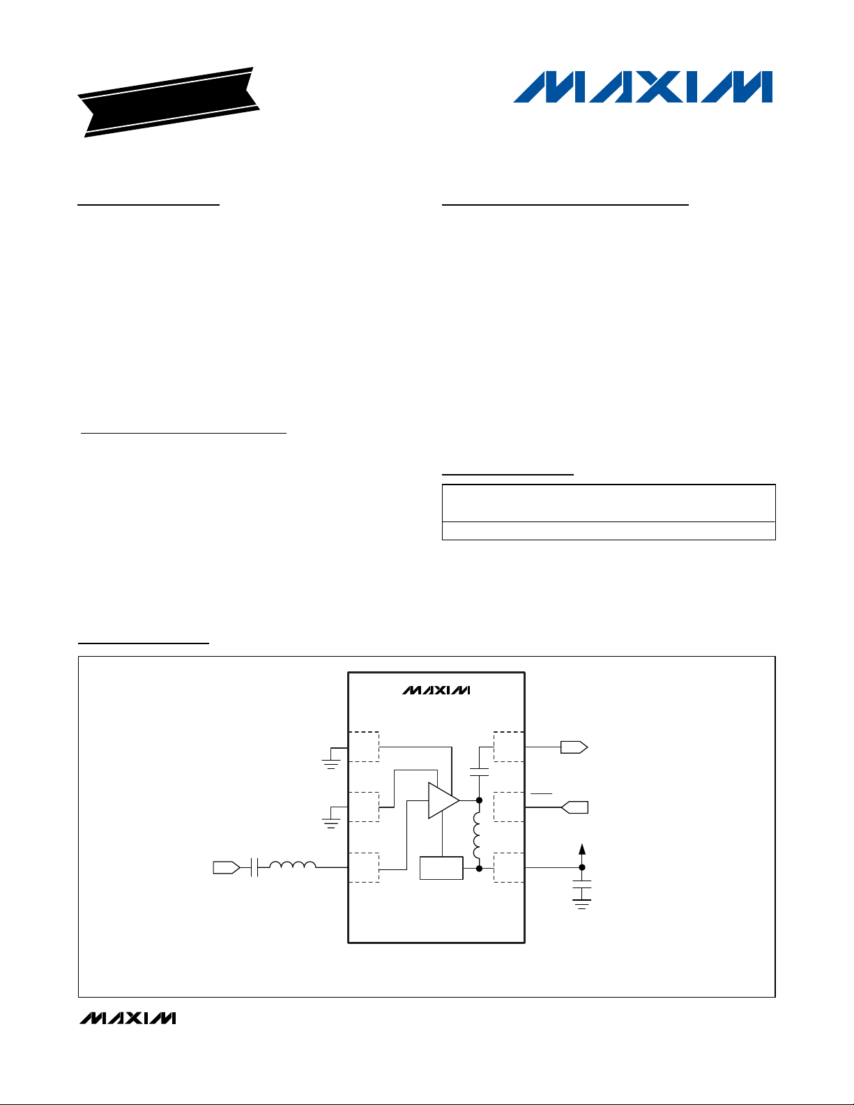
Pin Diagram/Functional Diagram/Typical Application Circuit
Ordering Information
19-0797; Rev 0; 4/07
For pricing, delivery, and ordering information, please contact Maxim/Dallas Direct! at
1-888-629-4642, or visit Maxim’s website at www.maxim-ic.com.
+
Denotes a lead-free package.
PART TEMP RANGE PIN-PACKAGE
PKG
CODE
MAX2659ELT+ -40°C to +85°C 6 µDFN L611-2
EVALUATION KIT
AVAILABLE
+
MAX2659
GND
1
GND
2
RF
INPUT
C1
RFIN
L1
3
BIAS
L1 = 6.8nH
C1 = 470pF
C2 = 33nF
RFOUT
6
SHDN
5
V
CC
4
RF
OUTPUT
LOGIC
CONTROL
V
CC
C2
Page 2
MAX2659
GPS/GNSS Low-Noise Amplifier
2 _______________________________________________________________________________________
ABSOLUTE MAXIMUM RATINGS
DC ELECTRICAL CHARACTERISTICS
(MAX2659 EV kit; VCC= 1.6V to 3.3V, TA= -40°C to +85°C, no RF signals are applied. Typical values are at VCC= 2.85V and
T
A
= +25°C, unless otherwise noted.) (Note 1)
Stresses beyond those listed under “Absolute Maximum Ratings” may cause permanent damage to the device. These are stress ratings only, and functional
operation of the device at these or any other conditions beyond those indicated in the operational sections of the specifications is not implied. Exposure to
absolute maximum rating conditions for extended periods may affect device reliability.
Note 1: Min and Max limits guaranteed by test at TA= +25°C and guaranteed by design and characterization at TA= -40°C and
T
A
= +85°C.
Note 2: Guaranteed by design and characterization.
Note 3: Measured with the two tones located at 5MHz and 10MHz offset from the center of the GPS band with -40dBm/tone.
Note 4: Measured with a tone located at 5MHz offset from the center of the GPS band.
V
CC
to GND...........................................................-0.3V to +4.2V
Other Pins to GND....................-0.3V to + Operating V
CC
+ 0.3V
Maximum RF Input Power .............................................+10dBm
Continuous Power Dissipation (T
A
= +70°C)
6-Pin µDFN (derates 2.1mW/°C above +70°C)............167mW
Operating Temperature Range ...........................-40°C to +85°C
Junction Temperature......................................................+150°C
Storage Temperature Range .............................-65°C to +160°C
Lead Temperature (soldering, 10s) .................................+260°C
AC ELECTRICAL CHARACTERISTICS
(MAX2659 EV kit; VCC= 1.6V to 3.3V, TA= -40°C to +85°C, f
RFIN
= 1575.42MHz. Typical values are at VCC= 2.85V and TA= +25°C,
unless otherwise noted.) (Note 1)
CAUTION! ESD SENSITIVE DEVICE
Supply Voltage 1.6 2.85 3.3 V
Supply Current
Digital Input-Logic High 1.4 V
Digital Input-Logic Low 0.4 V
Digital Input Current 1 µA
PARAMETER CONDITIONS MIN TYP MAX UNITS
SHDN = high 4.1 5.6 mA
Shutdown mode, SHDN = low 1 µA
PARAMETER CONDITIONS MIN TYP MAX UNITS
RF Frequency L1 band 1575.42 MHz
Power Gain
Noise Figure (Note 2) 0.8 dB
3rd-Order Input Intercept Point (Note 3) -5 dBm
Input 1dB Compression point (Note 4) -12 dBm
Input Return Loss (Note 2) 10 15 dB
Output Return Loss (Note 2) 10 25 dB
Reverse Isolation (Note 2) 32 dB
VCC = 2.85V 17 20.5
= 1.6V 16.5 20.5
V
CC
dB
Page 3
MAX2659
GPS/GNSS Low-Noise Amplifier
_______________________________________________________________________________________
3
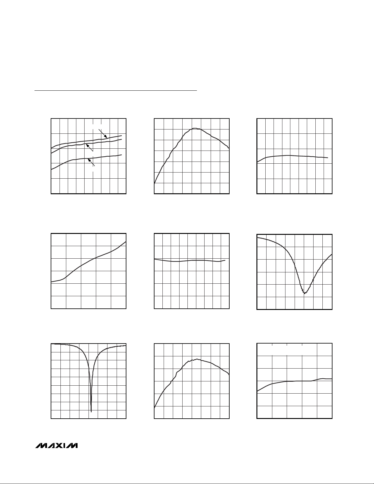
Typical Operating Characteristics
(MAX2659 EV kit; Typical values are at VCC= 2.85V, TA= +25°C, and f
RFIN
= 1575.42MHz, unless otherwise noted.)
SUPPLY CURRENT vs. SUPPLY VOLTAGE
4.5
+85°C
4.3
4.1
3.9
SUPPLY CURRENT (mA)
3.7
3.5
1.6 1.8 2.0 3.4
SUPPLY VOLTAGE (V)
+25°C
-40°C
2.8
NOISE FIGURE vs. TEMPERATURE
1.2
1.0
0.8
25
20
MAX2659 toc01
15
10
GAIN (dB)
5
0
-5
MAX2659 toc04
-10
1.2
1.0
0.8
3.0 3.22.62.42.2
GAIN vs. RF FREQUENCY
500 2500
RF FREQUENCY (MHz)
NOISE FIGURE vs. SUPPLY VOLTAGE
21.0
MAX2659 toc02
20.8
20.6
GAIN (dB)
20.4
20.2
MAX2659 toc05
20.0
-5
-10
2000 225017501250 1500750 1000
GAIN vs. SUPPLY VOLTAGE
1.6 3.43.2
SUPPLY VOLTAGE (V)
2.8 3.02.62.2 2.41.8 2.0
INPUT RETURN LOSS
vs. RF FREQUENCY
0
MAX2659 toc03
MAX2659 toc06
0.6
NOISE FIGURE (dB)
0.4
0.2
0
-40 85
TEMPERATURE (°C)
35 6010-15
OUTPUT RETURN LOSS
vs. RF FREQUENCY
0
-5
-10
-15
-20
-25
-30
-35
OUTPUT RETURN LOSS |S22| (dB)
-40
-45
500 2000 22501500750 2500
RF FREQUENCY (MHz)
175012501000
0.6
NOISE FIGURE (dB)
0.4
0.2
0
1.6 3.0 3.22.62.21.8 3.4
-20
-30
MAX2659 toc07
-40
-50
-60
REVERSE ISOLATION |S12| (dB)
-70
-80
500 2000 22501500750 2500
2.82.42.0
SUPPLY VOLTAGE (V)
REVERSE ISOLATION
vs. RF FREQUENCY
175012501000
RF FREQUENCY (MHz)
-15
-20
INPUT RETURN LOSS |S11| (dB)
-25
-30
500 2000 22501500750 2500
-3.5
TWO TONES LOCATED AT 5MHz AND
10MHz OFFSET WITH -40dBm/TONE
-4.0
MAX2659 toc08
-4.5
-5.0
IIP3 (dBm)
-5.5
-6.0
-6.5
-40 60 85
175012501000
RF FREQUENCY (MHz)
IIP3 vs. TEMPERATURE
MAX2659 toc09
3510-15
TEMPERATURE (°C)
Page 4

MAX2659
GPS/GNSS Low-Noise Amplifier
4 _______________________________________________________________________________________
Typical Operating Characteristics (continued)
(MAX2659 EV kit; Typical values are at VCC= 2.85V, TA= +25°C, and f
RFIN
= 1575.42MHz, unless otherwise noted.)
IIP3 vs. SUPPLY VOLTAGE
MAX2659 toc10
SUPPLY VOLTAGE (V)
IIP3 (dBm)
2.6 2.82.42.22.01.8
-7
-6
-4
-5
-3
-8
1.6 3.0 3.2 3.4
TWO TONES LOCATED AT 5MHz AND
10MHz OFFSET WITH -40dBm/TONE
INPUT P1dB COMPRESSION
vs. TEMPERATURE
MAX2659 toc11
TEMPERATURE (°C)
P1dB COMPRESSION (dBm)
3510-15
-14
-13
-10
-11
-12
-9
-15
-40 60 85
INPUT P1dB COMPRESSION
vs. SUPPLY VOLTAGE
MAX2659 toc12
SUPPLY VOLTAGE (V)
P1dB COMPRESSION (dBm)
2.82.4 2.61.8 2.0 2.2
-18
-16
-10
-12
-14
-8
-20
1.6 3.0 3.2 3.4
INPUT P1dB COMPRESSION
vs. JAMMER FREQUENCY
MAX2659 toc13
JAMMER FREQUENCY (MHz)
P1dB COMPRESSION (dBm)
17501500750 1000 1250
-25
-20
-5
-10
-15
0
-30
500 2000 2250 2500
NF vs. JAMMER POWER AT 850MHz
MAX2659 toc14
JAMMER POWER (dBm)
NF (dB)
-15-25 -20
0.5
1.0
1.5
3.0
2.5
2.0
3.5
0
-30 -10 -5
NF vs. JAMMER POWER AT 1850MHz
MAX2659 toc15
JAMMER POWER (dBm)
NF (dB)
-15-25 -20
0.5
1.0
1.5
3.0
2.5
2.0
3.5
0
-30 -10
Page 5

Detailed Description
The MAX2659 is an LNA designed for GPS L1,
GALILEO, and GLONASS applications. The device features a power-shutdown control mode to eliminate the
need for an external supply switch. The device
achieves a 20.5dB gain and an ultra-low-noise figure of
0.8dB. The MAX2659 consumes approximately 4.1mA
while providing a IP
1dB
of -12dBm and an IIP3 of -5dBm.
Input and Output Matching
The MAX2659 requires an off-chip input matching. Only
a 6.8nH inductor in series with a DC-blocking capacitor
is needed to form the input matching circuit. The
Typical Application Circuit
diagram shows the recommended input-matching network. These values are
optimized for the best simultaneous gain, noise figure,
and return loss performance. Table 1 lists typical
device S11 values. The MAX2659 integrates an on-chip
output matching to 50Ω at the output, eliminating the
need for external matching components.
Shutdown
The MAX2659 includes a shutdown feature to turn off
the entire chip. Apply a logic high to SHDN pin to place
the part in the active mode and a logic low to place the
part in the shutdown mode.
Applications Information
A properly designed PC board (PCB) is essential to any
RF microwave circuit. Use controlled-impedance lines
on all high-frequency inputs and outputs. Bypass V
CC
with decoupling capacitors located close to the device.
For long VCClines, it may be necessary to add decoupling capacitors. Locate these additional capacitors
further away from the device package. Proper grounding of the GND pins is essential. If the PCB uses a topside RF ground, connect it directly to the GND pins. For
a board where the ground is not on the component
layer, connect the GND pins to the board with multiple
vias close to the package.
Chip Information
PROCESS: SiGe BiCMOS
MAX2659
GPS/GNSS Low-Noise Amplifier
_______________________________________________________________________________________ 5
Pin Description
PIN NAME FUNCTION
1, 2 GND Ground. Connect to the PCB ground plane.
3 RFIN RF Input. Requires a DC-blocking capacitor and external matching components.
4 VCC Suppl y Voltage. Bypa ss to ground with a 33nF capacitor as close a s possible to the IC.
5 SHDN Shutdown Input. A logic-low disab les the device.
6 RFOUT RF Output. RFOUT is internally matched to 50 and incorporates an internal DC-blocking capacitor.
Table 1. Typical S11 Values
FREQUENCY (MHz) REAL S11 IMAGINARY S11
1000 -0.58 -j0.52
1100 -0.68 -j0.356
1200 -0.74 -j0.16
1300 -0.74 j0.036
1400 -0.676 j0.22
1500 -0.56 j0.36
1575 -0.47 j0.415
1600 -0.44 j0.43
1700 -0.36 j0.467
1800 -0.3 j0.51
1900 -0.228 j0.567
2000 -0.14 j0.622
Page 6

MAX2659
GPS/GNSS Low-Noise Amplifier
6 _______________________________________________________________________________________
Package Information
(The package drawing(s) in this data sheet may not reflect the most current specifications. For the latest package outline information
go to www.maxim-ic.com/packages
.)
L
TOP VIEW
D
E
SIDE VIEW
A1
A
A 0.65
COMMON DIMENSIONS
PIN 1
0.075x45∞
BOTTOM VIEW
L1
32
MIN.
1
e
6
5
b
4
SECTION A-A
b
L2
A A
NOM.
0.72 0.80
MAX.
0.00
A1
0.05
1.501.45D 1.55
1.000.95E 1.05
0.350.30L 0.40
--0.00
L1
0.08
--0.05L2 0.10
0.200.17b 0.23
0.50 BSC.e
AA
TOPMARK
2
1
-DRAWING NOT TO SCALE-
DOCUMENT CONTROL NO.APPROVAL
TITLE:
REV.
PACKAGE OUTLINE, 6L uDFN, 1.5x1.0x0.8mm
21-0147
2
1
E
3
PIN 1
MARK
4
5
L611-1, L611-2
Pkg.
Code
--
--
A2
0.20 --
A2
6L UDFN.EPS
Page 7

MAX2659
GPS/GNSS Low-Noise Amplifier
Maxim cannot assume responsibility for use of any circuitry other than circuitry entirely embodied in a Maxim product. No circuit patent licenses are
implied. Maxim reserves the right to change the circuitry and specifications without notice at any time.
Maxim Integrated Products, 120 San Gabriel Drive, Sunnyvale, CA 94086 408-737-7600 _____________________
7
© 2007 Maxim Integrated Products is a registered trademark of Maxim Integrated Products, Inc.
Package Information (continued)
(The package drawing(s) in this data sheet may not reflect the most current specifications. For the latest package outline information
go to www.maxim-ic.com/packages
.)
-DRAWING NOT TO SCALE-
DOCUMENT CONTROL NO.APPROVAL
TITLE:
REV.
PACKAGE OUTLINE, 6L uDFN, 1.5x1.0x0.8mm
21-0147
2
2
E
2005 2006 2007 2008 2009 2010 2011 2012 2013 2014Calendar Year
Legend:
Marked with bar Blank space - no bar required
06-11Payweek 12-17 18-23 24-29 30-35 36-41 42-47 48-51 52-05
TABLE 2 Translation Table for Payweek Binary Coding
TABLE 1 Translation Table for Calendar Year Code
Legend: Marked with bar Blank space - no bar required
 Loading...