Page 1
General Description
The MAX2654/MAX2655/MAX2656 high third-order
intercept point (IP3), low-noise amplifiers (LNAs) are
designed for applications in GPS, PCS, WLL, and satellite phone systems. The MAX2654/MAX2655/MAX2656
incorporate on-chip internal output matching to 50Ω,
eliminating the need for external matching components.
A shutdown feature in the MAX2654/MAX2655 reduces
the operating current to 0.1µA, eliminating the need for
an external supply switch.
The MAX2654 operates in the GPS frequency of
1575MHz with 15.1dB of gain, 1.5dB noise figure, and
only consumes 5.8mA. The MAX2655 is designed with
high-input IP3 to improve operation in cellular applications where the cellular power amplifier leaks into the
GPS receiver. The MAX2656 is designed for PCS
phone applications with 13.5dB of gain in high-gain
mode and 0.8dB of gain in low-gain mode (selected by
a logic control) and 1.9dB noise figure.
The IP3 of MAX2655/MAX2656 is adjustable by a single
external bias resistor (R
BIAS
), allowing supply current to
be optimized for a specific application.
The MAX2654/MAX2655/MAX2656 operate from a
+2.7V to +5.5V single supply and are available in the
miniature 6-pin SC70 package.
________________________Applications
GPS Receivers
GPS Receivers in Cellular Phones
DCS/PCS Cellular Phones
Satellite Phones
Wireless Local Loop
Features
♦ Low Noise Figure
MAX2654: 1.5dB at 1575MHz
MAX2655: 1.45dB at 1575MHz
MAX2656: 1.9dB at 1960MHz
♦ High Gain
MAX2654: 15.1dB at 1575MHz
MAX2655: 14.1dB at 1575MHz
MAX2656: 13.5dB at 1960MHz
♦ 12.7dB Gain Step (MAX2656 only)
♦ Integrated 50Ω Output Matching
♦ Variable IP3 Set by One Bias Resistor
(MAX2655/MAX2656 only)
♦ 0.1µA Shutdown Mode (MAX2654/MAX2655 only)
♦ +2.7V to +5.5V Single-Supply Operation
♦ Ultra-Small 6-Pin SC70 Package
MAX2654/MAX2655/MAX2656
1575MHz/1900MHz Variable-IP3
Low-Noise Amplifiers
________________________________________________________________ Maxim Integrated Products 1
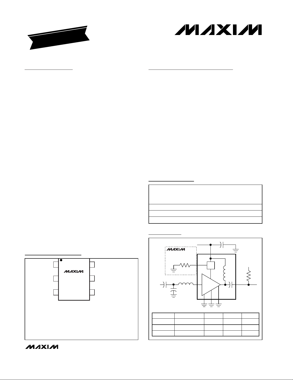
Pin Configuration
MAX2655
MAX2656
C2
3
4
6
10kΩ
Cb
(1)
1
25
C1
R
BIAS
V
CTRL
/GND
V
CC
= +3V
RFOUT
RFIN
L1
BIAS
( ) ARE FOR MAX2654 ONLY
Typical Operating Circuit
19-1872; Rev 1; 4/02
EVALUATION KIT
AVAILABLE
Ordering Information
For pricing, delivery, and ordering information, please contact Maxim/Dallas Direct! at
1-888-629-4642, or visit Maxim’s website at www.maxim-ic.com.
PART
MAX2654EXT-T -40°C to +85°C
MAX2655EXT-T -40°C to +85°C
MAX2656EXT-T -40°C to +95°C
TEMP
RANGE
PIN-
PACKAGE
6 SC70-6
6 SC70-6
6 SC70-6
SOT
TOP-
MARK
AAI
AAJ
AAK
ARE FOR MAX2654 ONLY
BIAS (GND)
5
RFOUT
GND
V
CC
16
MAX2654
2
GND
RFIN
MAX2655
MAX2654
34
SC70-6
PART FREQUENCY L1 (nH) C1 (pF) C2 (pF)
MAX2654 1575 5.6 6 1.6
MAX2655 1575 5.6 1800 1.5
MAX2656 1960 4.7 1800 1.2
Page 2
MAX2654/MAX2655/MAX2656
1575MHz/1900MHz Variable-IP3
Low-Noise Amplifiers
2 _______________________________________________________________________________________
ABSOLUTE MAXIMUM RATINGS
Stresses beyond those listed under “Absolute Maximum Ratings” may cause permanent damage to the device. These are stress ratings only, and functional
operation of the device at these or any other conditions beyond those indicated in the operational sections of the specifications is not implied. Exposure to
absolute maximum rating conditions for extended periods may affect device reliability.
VCCto GND .............................................................-0.3V to +6V
RF Input Power .................................................................+5dBm
Continuous Power Dissipation (T
A
= +70°C)
6-Pin SC70 (derate 3.1mW/°C above +70°C)..............245mW
Operating Temperature Range ...........................-40°C to +85°C
Maximum Junction Temperature .....................................+150°C
Storage Temperature.........................................-65°C to +150°C
Lead Temperature (soldering, 10s) .................................+300°C
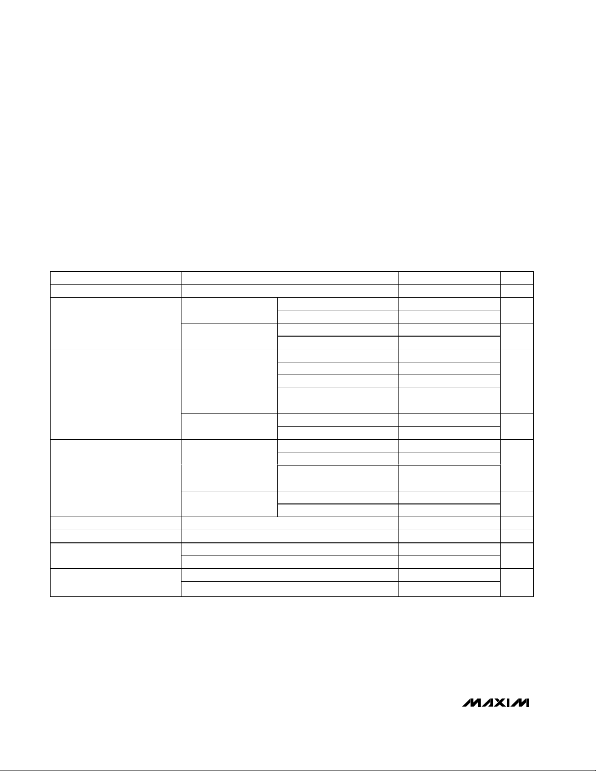
DC ELECTRICAL CHARACTERISTICS
(V
CC
= +2.7V to +5.5V, R
BIAS
= 511Ω ±1%, TA= -40°C to +85°C. No RF signal applied. RFIN is AC-coupled and terminated to 50Ω.
RFOUT is unconnected. Typical values are at V
CC
= +3V, TA= +25°C, unless otherwise noted.) (Note 1)
PARAMETER CONDITIONS MIN TYP MAX UNIT
Supply Voltage 2.7 5.5 V
Operating Supply Current
(MAX2654 only)
Operating Supply Current
RFOUT
V
RFOUT
V
RFOUT
T
= +25°C
A
CC
= GND
= V
CC
V
= V
(MAX2655 only)
V
= GND
RFOUT
= GND
V
RFOUT
= +25°C
T
A
Operating Supply Current
(MAX2656 only)
Input Logic High at V
Input Logic Low at V
RFOUT
RFOUT
Input Logic High Current
at V
RFOUT
(Note 4)
Input Logic Low Current
at V
RFOUT
(Note 5)
V
= V
RFOUT
CC
(Note 2) 2 V
(Note 3) 0.6 V
MAX2654/MAX2655 15.6
MAX2656 71
MAX2654/MAX2655 1
MAX2656 -24
TA = +25°C 5.8 8.2
TA = -40°C to +85°C 9.2
TA = +25°C 0.1 1
= -40°C to +85°C 2.1
T
A
R
= 511Ω ±1% 8.3 10
BIAS
R
= 698Ω ±1% 5.9
BIAS
R
= 357Ω ±1% 10.1
BIAS
R
= 511Ω ±1%,
BIAS
= -40°C to +85°C
T
A
11.1
TA = +25°C 0.1 1
T
= -40°C to +85°C 2.2
A
R
= 511Ω ±1% 11.5 15.2
BIAS
R
= 715Ω ±1% 8.5
BIAS
R
= 511Ω ±1%,
BIAS
T
= +85°C
A
13.6
TA = +25°C 12.3
TA = +85°C 14.6
mA
µA
mA
µA
mA
mA
µA
µA
Page 3
MAX2654/MAX2655/MAX2656
1575MHz/1900MHz Variable-IP3
Low-Noise Amplifiers
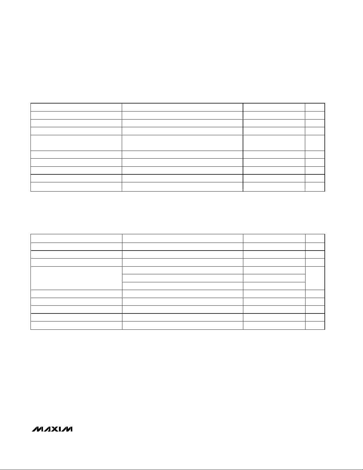
AC ELECTRICAL CHARACTERISTICS (MAX2654)
(MAX2654 Evaluation Kit, VCC= +3.0V, PIN= -30dBm, f
IN
= 1575MHz, V
RFOUT
= VCCthrough a 10kΩ resistor, TA= +25°C. Typical
values are at V
CC
= +3V, TA= +25°C, unless otherwise noted.) (Note 6)
AC ELECTRICAL CHARACTERISTICS (MAX2655)
(MAX2655 Evaluation Kit, VCC= +3.0V, PIN= -30dBm, f
IN
= 1575MHz, V
RFOUT
= VCCthrough a 10kΩ resistor, R
BIAS
= 511Ω ±1%,
T
A
= +25°C. Typical values are at VCC= +3V, TA= +25°C, unless otherwise noted.) (Note 6)
_______________________________________________________________________________________ 3
Operating Frequency Range (Note 7) 1400 1700 MHz
Gain (Note 8) 12.7 15.1 dB
Gain Variation Over Temperature TA = -40°C to +85°C 0.15 1 dB
Input Third-Order Intercept Point
(Note 9)
Input 1dB Compression Point -18 dBm
Noise Figure (Note 10) 1.5 1.8 dB
Input Return Loss 9.7 dB
Output Return Loss 8.4 dB
Reverse Isolation 30 dB
PARAMETER CONDITIONS MIN TYP MAX UNIT
-7.2 dBm
Operating Frequency Range (Note 7) 1400 1700 MHz
Gain (Note 8) 12 14.1 dB
Gain Variation Over Temperature TA = -40°C to +85°C 0.6 1.1 dB
Input Third-Order Intercept Point
(Note 9)
Input 1dB Compression Point -12.2 dBm
Noise Figure (Note 10) 1.45 1.9 dB
Input Return Loss 16.1 dB
Output Return Loss 15.5 dB
Reverse Isolation 32 dB
PARAMETER CONDITIONS MIN TYP MAX UNIT
R
= 511Ω ±1% 2.8
BIAS
R
= 698Ω ±1% 2.2 dBm
BIAS
R
= 357Ω ±1% 3.8
BIAS
Page 4
MAX2654/MAX2655/MAX2656
1575MHz/1900MHz Variable-IP3
Low-Noise Amplifiers
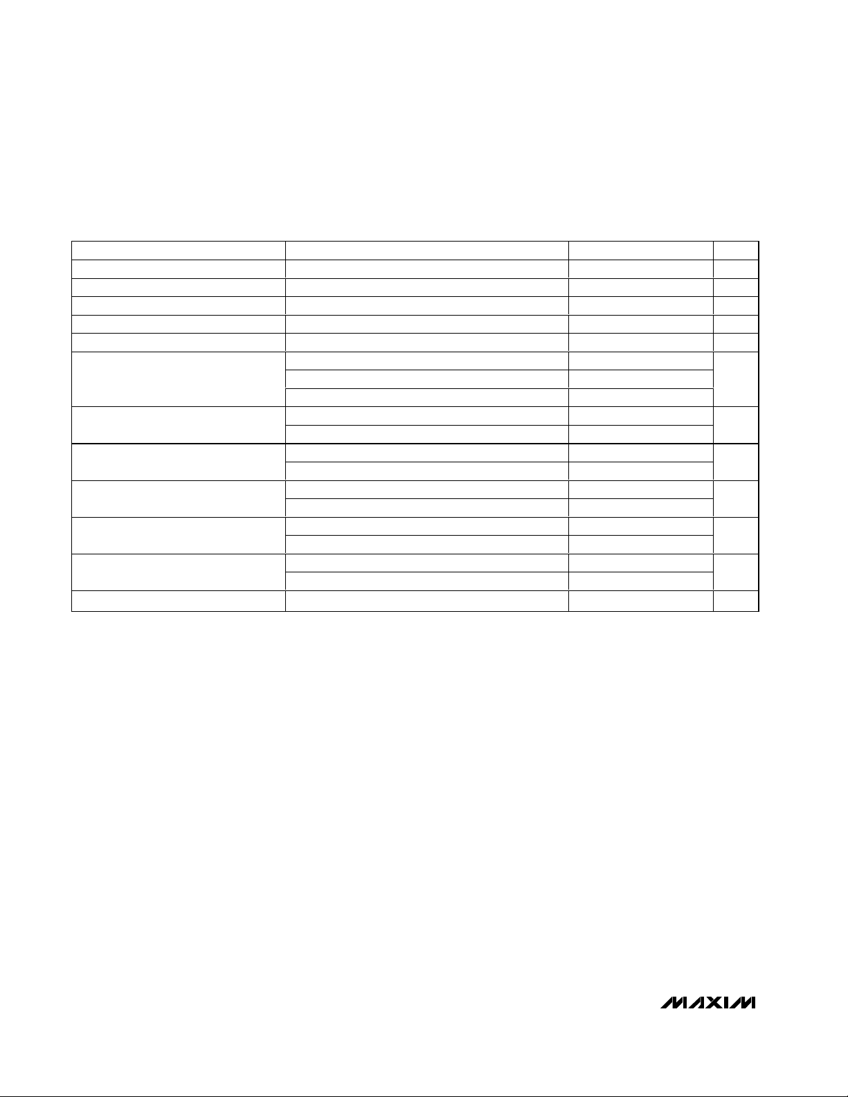
AC ELECTRICAL CHARACTERISTICS (MAX2656)
(MAX2656 Evaluation Kit, VCC= +3V, PIN= -30dBm, f
IN
= 1960MHz, V
RFOUT
= GND through a 12kΩ resistor, R
BIAS
= 511Ω ±1%, T
A
= +25°C. Typical values are at VCC= +3V, TA= +25°C, unless otherwise noted.) (Note 6)
Note 1: Devices are production tested at TA= +25°C. Minimum and maximum values are guaranteed by design and characteriza-
tion over temperature and supply voltages to ±6 sigma.
Note 2: Minimum DC voltage through a 10kΩ resistor that sets the MAX2654/MAX2655 to operate in normal mode and MAX2656 in
low-gain mode.
Note 3: Maximum DC voltage through a 10kΩ resistor that sets the MAX2654/MAX2655 to operate in shutdown mode and
MAX2656 in high-gain mode.
Note 4: DC current required when V
RFOUT
is connected to VCCthrough a 10kΩ resistor.
Note 5: DC current required when V
RFOUT
is connected to GND through a 10kΩ resistor.
Note 6: Guaranteed by design and characterization to ±3 sigma.
Note 7: The part has been characterized at the specified frequency range. Operation outside of this range is possible, but not
guaranteed.
Note 8: Production tested at T
A
= +25°C.
Note 9: Measured with two input tones, f
1
= 1570MHz, f2= 1580MHz, both at -30dBm per tone.
Note 10: Excludes PC board losses of 0.2dB for MAX2654/MAX2655 and 0.25dB for MAX2656.
Note 11: High-gain mode is set up by connecting RFOUT to GND through a 12kΩ resistor.
Note 12: Low-gain mode is set up by connecting RFOUT to V
CC
through a 12kΩ resistor.
Note 13: Measured with two input tones, f
1
= 1955MHz, f2= 1965MHz, both at -30dBm per tone.
4 ______________________________________________________________________________________
Operating Frequency Range (Note 7) 1800 2000 MHz
Gain, High-Gain Mode (Note 11) 12 13.5 dB
Gain, Low-Gain Mode (Note 12) 0.8 dB
Gain Variation Over Temperature TA = -40°C to +85°C 0.3 1.2 dB
Gain Step 12.7 dB
Input Third-Order Intercept Point
(Note 13)
Input 1dB Compression Point
Noise Figure (Note 10)
Input Return Loss
Output Return Loss
Reverse Isolation
Gain Step Response Time 3.2 µs
PARAMETER CONDITIONS MIN TYP MAX UNIT
R
BIAS
R
BIAS
Low-gain mode (Note 12) 7.2
High-gain mode (Note 11) -7
Low-gain mode (Note 12) -1.2
High-gain mode (Note 11) 1.9 2.4
Low-gain mode (Note 12) 10.8
High-gain mode (Note 11) 14.4
Low-gain mode (Note 12) 19.3
High-gain mode (Note 11) 10.7
Low-gain mode (Note 12) 7.3
High-gain mode (Note 11) 28
Low-gain mode (Note 12) 25
= 511Ω ± 1% 1.5
= 715Ω ± 1% -3
dBm
dBm
dB
dB
dB
dB
Page 5
MAX2654/MAX2655/MAX2656
1575MHz/1900MHz Variable-IP3
Low-Noise Amplifiers
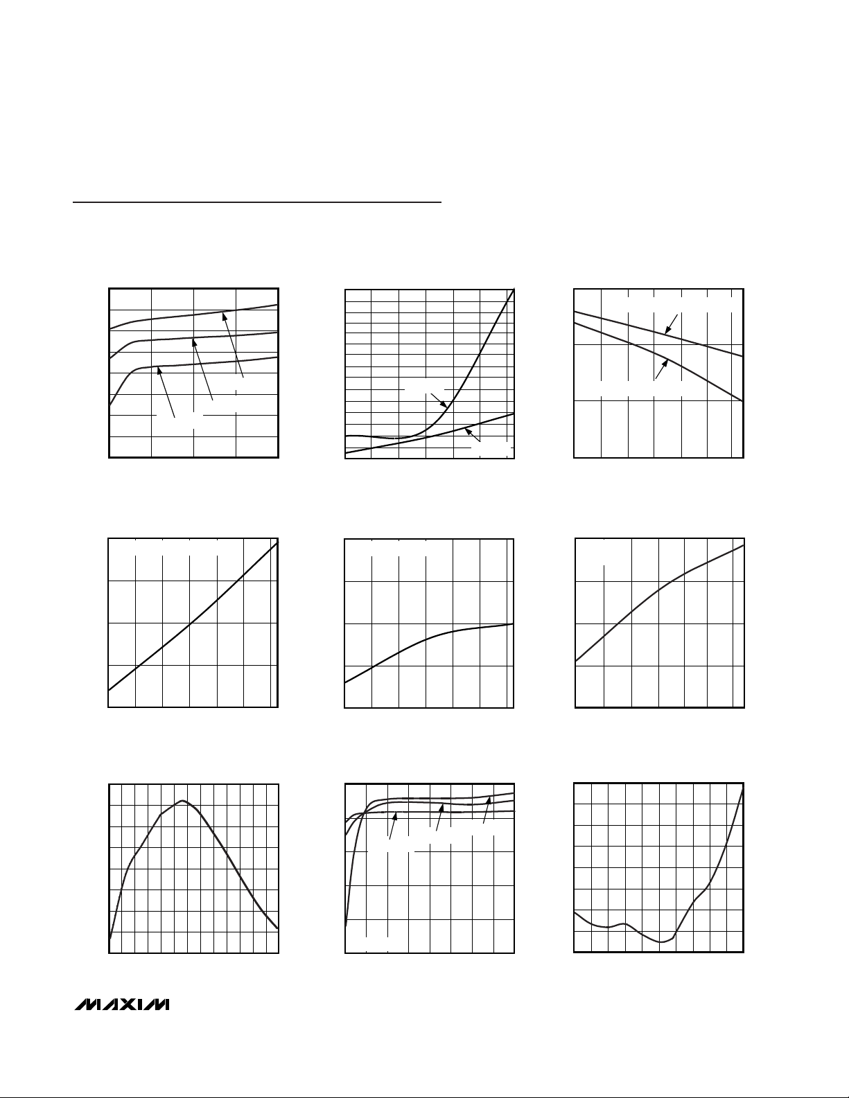
Typical Operating Characteristics
(PIN= -30dBm, input and output are terminated to 50Ω, VCC= +3V, high-gain and low-gain modes are applicable only to the MAX2656,
T
A
= +25°C, unless otherwise noted.)
0
1
2
3
4
5
6
7
8
23456
MAX2654
SUPPLY CURRENT vs. SUPPLY VOLTAGE
MAX2654 toc01
SUPPLY VOLTAGE (V)
SUPPLY CURRENT (mA)
TA = -40°C
TA = +25°C
TA = +85°C
40
45
50
55
60
-40 0 20-20 40 60 80
MAX2654
INPUT LOGIC CURRENT vs. TEMPERATURE
MAX2654 toc05
TEMPERATURE (°C)
INPUT LOGIC CURRENT (µA)
INPUT LOGIC LOW AT V
RFOUT
0
6
4
2
8
10
14
12
16
1000 1200 1400 1600 1800 2000 2200
MAX2654
GAIN vs. FREQUENCY
MAX2654 toc07
FREQUENCY (MHz)
GAIN (dB)
1.6
2.0
1.8
2.2
2.8
3.0
2.6
2.4
3.2
1000 1200 1400 1600 1800 2000
MAX2654
NOISE FIGURE vs. FREQUENCY
MAX2654 toc09
FREQUENCY (MHz)
NOISE FIGURE (dB)
0
4
6
7
8
-40 0 20-20 40 60 80
MAX2654
INPUT LOGIC CURRENT vs. TEMPERATURE
MAX2654 toc04
TEMPERATURE (°C)
INPUT LOGIC CURRENT (µA)
INPUT LOGIC HIGH AT V
RFOUT
10
11
13
12
14
15
2.0 3.0 3.52.5 4.0 4.5 5.0 5.5 6.0
MAX2654
GAIN vs. SUPPLY VOLTAGE
MAX2654 toc08
SUPPLY VOLTAGE (V)
GAIN (dB)
f0 = 1575MHz
TA = +85°C
TA = +25°C
TA = -40°C
4
6
8
10
12
14
-40 -20 0 20 40 8060
MAX2654
SHUTDOWN CURRENT vs. TEMPERATURE
MAX2654 toc02
TEMPERATURE (°C)
SHUTDOWN CURRENT (µA)
2
0
VCC = +6V
VCC = +3V
-40 0-20 20 40 60 80
MAX2654
INPUT LOGIC VOLTAGE vs. TEMPERATURE
MAX2654 toc03
TEMPERATURE (°C)
INPUT LOGIC VOLTAGE (V)
0.5
1.0
1.5
2.0
INPUT LOGIC HIGH AT V
RFOUT
INPUT LOGIC LOW AT V
RFOUT
_______________________________________________________________________________________ 5
INPUT IP3 vs. TEMPERATURE
-6
f1 = 1570 MHz
= 1580 MHz
f
2
-7
MAX2654
MAX2654 toc06
-8
INPUT IP3 (dBm)
-9
-10
-40 20 40-20 0 60 80
TEMPERATURE (°C)
Page 6

MAX2654/MAX2655/MAX2656
1575MHz/1900MHz Variable-IP3
Low-Noise Amplifiers
-10
-8
-6
-4
-2
0
1000 1200 1400 1600 1800 2000
MAX2654
INPUT/OUTPUT RETURN LOSS vs. FREQUENCY
MAX2654 toc11
FREQUENCY (MHz)
INPUT/OUTPUT RETURN LOSS (dB)
2200
INPUT RETURN LOSS
OUTPUT RETURN LOSS
-60
-45
-50
-55
-40
-35
-25
-30
-20
1000 1200 1400 1600 1800 2000 2200
MAX2654
REVERSE ISOLATION vs. FREQUENCY
MAX2654 toc12
FREQUENCY (MHz)
REVERSE ISOLATION (dB)
-14
-10
-12
-8
-6
-4
-2
0
2
4
6
8
-30 -26 -22 -18 -14 -10
MAX2654
OUTPUT POWER vs. INPUT POWER
MAX2654 toc13
INPUT POWER (dBm)
OUTPUT POWER (dBm)
-16
-6 -2 2
6 ______________________________________________________________________________________
Typical Operating Characteristics (continued)
(PIN= -30dBm, input and output are terminated to 50Ω, VCC= +3V, high-gain and low-gain modes are applicable only to the MAX2656,
T
A
= +25°C, unless otherwise noted.)
1.0
1.4
1.2
1.8
1.6
2.2
2.0
2.4
-40 0 20-20 40 60 80
MAX2654
NOISE FIGURE vs. TEMPERATURE
MAX2654 toc10
NOISE FIGURE (dB)
fIN = 1575MHz
-100
-90
-80
-70
-50
-60
-40
-20
-30
-10
0
0 1.0 2.0 3.0 4.0
MAX2654
SHUTDOWN TIME
MAX2655 toc15
TIME (µs)
OUTPUT POWER (dBm)
2.8µs
US
MAX2654
vs. TEMPERATURE
P
-17
-18
1dB
fIN = 1575MHz
MAX2654 toc14
SUPPLY CURRENT vs. SUPPLY VOLTAGE
8
R
BIAS
7
6
5
4
3
SUPPLY CURRENT (mA)
2
TA = -40°C
1
0
23456
MAX2655
= 698Ω ±1%
TA = +25°C
TA = +85°C
-19
(dBm)
1dB
P
-20
-21
-22
10
9
MAX2655 toc16
8
7
6
5
4
3
SUPPLY CURRENT (mA)
2
1
0
-40 0-20 20 40 60 80
TEMPERATURE (°C)
MAX2655
SUPPLY CURRENT vs. SUPPLY VOLTAGE
R
= 511Ω ±1%
BIAS
MAX2655 toc17
TA = +85°C
TA = +25°C
TA = -40°C
23456
SUPPLY CURRENT vs. SUPPLY VOLTAGE
MAX2655
14
R
= 357Ω ±1%
BIAS
12
10
8
6
SUPPLY CURRENT (mA)
4
2
0
TA = -40°C
23456
TA = +25°C
SUPPLY VOLTAGE (V)
TA = +85°C
MAX2655 toc18
Page 7

MAX2654/MAX2655/MAX2656
1575MHz/1900MHz Variable-IP3
Low-Noise Amplifiers
MAX2655
INPUT IP3 vs. R
BIAS
MAX2655 toc23
-10
-4
-6
-8
0
-2
6
8
4
2
10
INPUT IP3 (dBm)
200 600 800400
1000
1200 1400 1600
TEMPERATURE (°C)
TA = +85°C
PIN = -30dBm
f
1
= 1570MHz
f
2
= 1580MHz
TA = +25°C
TA = -40°C
Typical Operating Characteristics (continued)
(PIN= -30dBm, input and output are terminated to 50Ω, VCC= +3V, high-gain and low-gain modes are applicable only to the MAX2656,
TA= +25°C, unless otherwise noted.)
-40 0 20-20 40 60 80
MAX2655
INPUT LOGIC VOLTAGE vs. TEMPERATURE
MAX2655 toc21
TEMPERATURE (°C)
INPUT LOGIC VOLTAGE (V)
0.5
1.0
1.5
2.0
INPUT LOGIC HIGH AT V
RFOUT
INPUT LOGIC LOW AT V
RFOUT
10
11
13
12
14
15
2.0 3.0 3.52.5 4.0 4.5 5.0 5.5 6.0
MAX2655 toc26
SUPPLY VOLTAGE (V)
GAIN (dB)
TA = -40°C
TA = +85°C
TA = +25°C
fIN = 1575MHz
R
BIAS
= 511Ω ±1%
MAX2655
GAIN vs. SUPPLY VOLTAGE
1.4
1.8
1.6
2.2
2.0
2.6
2.4
2.8
3.2
3.0
3.4
1000 1200 1400 1600 1800 2000
MAX2655
NOISE FIGURE vs. FREQUENCY
MAX2655 toc27
FREQUENCY (MHz)
NOISE FIGURE (dB)
R
BIAS
= 357Ω ±1%
R
BIAS
= 511Ω ±1%
R
BIAS
= 698Ω ±1%
8
11
10
9
13
12
17
16
15
14
18
200 400 600 800 1000 1200 1400 1600
MAX2655
GAIN vs. R
BIAS
MAX2655 toc25
R
BIAS
(Ω)
GAIN (dB)
fIN = 1575MHz
TA = -40°C
TA = +85°C
TA = +25°C
MAX2655
INPUT LOGIC CURRENT vs. TEMPERATURE
MAX2655 toc22
4
5
6
9
8
7
10
INPUT LOGIC CURRENT (µA)
-40 0 20-20
40
60 80
TEMPERATURE (°C)
INPUT LOGIC HIGH AT V
RFOUT
INPUT LOGIC LOW AT V
RFOUT
0
6
4
2
8
10
12
14
16
1000 1400 16001200 1800 2000 2200
MAX2655
GAIN vs. FREQUENCY
MAX2655 toc24
FREQUENCY (MHz)
GAIN (dB)
R
BIAS
= 511Ω ±1%
R
BIAS
= 357Ω ±1%
R
BIAS
= 698Ω ±1%
_______________________________________________________________________________________ 7
SUPPLY CURRENT vs. R
16
14
12
10
SUPPLY CURRENT (mA)
TA = -40°C
8
6
4
2
0
200 600 800400
MAX2655
TA = +25°C
R
BIAS
TA = +85°C
1200 1400 1600
1000
(Ω)
BIAS
28
MAX2655 toc19
24
20
16
12
8
SHUTDOWN CURRENT (nA)
4
0
-40 0 20-20 40 60 80
SHUTDOWN CURRENT vs. TEMPERATURE
MAX2655
MAX2655 toc20
VCC = +6V
VCC = +3V
TEMPERATURE (°C)
Page 8

MAX2654/MAX2655/MAX2656
1575MHz/1900MHz Variable-IP3
Low-Noise Amplifiers
8 _______________________________________________________________________________________
Typical Operating Characteristics (continued)
(PIN= -30dBm, input and output are terminated to 50Ω, VCC= +3V, high-gain and low-gain modes are applicable only to the MAX2656,
T
A
= +25°C, unless otherwise noted.)
-4
-8
-12
-16
0
4
8
12
-30 -22 -18-26 -14 -10 -6 -2 2
MAX2655
OUTPUT POWER vs. INPUT POWER
MAX2655 toc32
INPUT POWER (dBm)
OUTPUT POWER (dBm)
fIN = 1575MHz
R
BIAS
= 698Ω ±1%
R
BIAS
= 357Ω ±1%
R
BIAS
= 511Ω ±1%
-18
-15
-16
-17
-13
-14
-9
-10
-11
-12
-8
200 400 600 800 1000 1200 1400 1600
MAX2655
P
1dB
vs. R
BIAS
MAX2655 toc33
R
BIAS
(Ω)
P
1dB
(dBm)
fIN = 1575MHz
TA = -40°C
TA = +85°C
TA = +25°C
0
4
2
6
8
10
12
14
23456
MAX2656
SUPPLY CURRENT vs. SUPPLY VOLTAGE
MAX2654 toc35
SUPPLY VOLTAGE (V)
SUPPLY CURRENT (mA)
R
BIAS
= 511Ω ±1%
HIGH-GAIN MODE
TA = +85°C
TA = +25°C
TA = -40°C
0
6
4
2
8
10
12
14
16
18
23456
MAX2656
SUPPLY CURRENT vs. SUPPLY VOLTAGE
MAX2654 toc36
SUPPLY VOLTAGE (V)
SUPPLY CURRENT (mA)
TA = +85°C
TA = +25°C
TA = -40°C
R
BIAS
= 392Ω ±1%
HIGH-GAIN MODE
0
3
2
1
4
5
6
7
8
9
10
23456
MAX2656
SUPPLY CURRENT vs. SUPPLY VOLTAGE
MAX2654 toc34
SUPPLY VOLTAGE (V)
SUPPLY CURRENT (mA)
R
BIAS
= 715Ω ±1%
HIGH-GAIN MODE
TA = +85°C
TA = +25°C
TA = -40°C
-24
-20
-16
-12
-8
-4
0
1000 1200 1400 1600 1800 2000
MAX2655
INPUT/OUTPUT RETURN LOSS vs. FREQUENCY
MAX2655 toc29
FREQUENCY (MHz)
INPUT/OUTPUT RETURN LOSS (dB)
2200
INPUT RETURN LOSS
OUTPUT RETURN LOSS
MAX2655
REVERSE ISOLATION vs. FREQUENCY
MAX2655 toc30
-60
-55
-45
-50
-30
-25
-35
-40
-20
REVERSE ISOLATION (dB)
1000 1400 16001200
1800
2000 2200
FREQUENCY (MHz)
1.0
1.2
1.6
1.4
1.8
2.0
-40 0-20 20 40 60 80
MAX2655
NOISE FIGURE vs. TEMPERATURE
MAX2655 toc28
TEMPERATURE (°C)
NOISE FIGURE (dB)
fIN = 1575MHz
R
BIAS
= 511Ω ±1%
MAX2655
0
-10
-20
-30
-40
-50
-60
-70
OUTPUT POWER (dBm)
-80
-90
-100
0 2.01.0 4.03.0 6.0 7.05.0 8.0
SHUTDOWN TIME
MAX2655 toc31
5.8µs
TIME (us)
Page 9

MAX2654/MAX2655/MAX2656
1575MHz/1900MHz Variable-IP3
Low-Noise Amplifiers
_______________________________________________________________________________________ 9
Typical Operating Characteristics (continued)
(PIN= -30dBm, input and output are terminated to 50Ω, VCC= +3V, high-gain and low-gain modes are applicable only to the MAX2656,
TA= +25°C, unless otherwise noted.)
0
8
4
16
12
24
20
200 600 800400 1000 1200 1400 1600
MAX2656
SUPPLY CURRENT vs. R
BIAS
MAX2654 toc41
R
BIAS
(Ω)
SUPPLY CURRENT (mA)
LOW-GAIN MODE
TA = +85°C
TA = -40°C
TA = +25°C
2.0
1.5
1.0
0.5
-40 20
-20
04060
MAX2656
INPUT LOGIC VOLTAGE vs. TEMPERATURE
MAX2654 toc42
TEMPERATURE (°C)
INPUT LOGIC VOLTAGE (V)
80
I
NPUT LOGIC HIGH AT V
RFOUT
INPUT LOGIC LOW AT V
RFOUT
-15
-11
-9
-13
-3
-7
-5
3
-1
1
5
200 600 800400 1000 1200 1400 1600
MAX2656
INPUT IP3 vs. R
BIAS
MAX2654 toc44
R
BIAS
(Ω)
INPUT IP3 (dBm)
TA = -40°C
TA = +85°C
f1 = 1955MHz
f
2
= 1965MHz
P
IN
= -20dBm
HIGH-GAIN MODE
TA = +25°C
-6
4
10
6
8
12
0
-4
-2
2
200 600 800400 1000 1200 1400 1600
MAX2656
INPUT IP3 vs. R
BIAS
MAX2654 toc45
R
BIAS
(Ω)
INPUT IP3 (dBm)
f1 = 1955MHz
f
2
= 1965MHz
P
IN
= -20dBm
LOW-GAIN MODE
TA = +25°C
TA = +85°C
TA = -40°C
10
0
-10
-20
-30
-40 20
-20
04060
MAX2656
INPUT LOGIC CURRENT vs. TEMPERATURE
MAX2654 toc43
TEMPERATURE (°C)
INPUT LOGIC CURRENT (µA)
80
INPUT LOGIC LOW AT V
RFOUT
I
NPUT LOGIC HIGH AT V
RFOUT
0
10
12
14
16
2
4
6
8
23456
MAX2656
SUPPLY CURRENT vs. SUPPLY VOLTAGE
MAX2654 toc38
SUPPLY VOLTAGE (V)
SUPPLY CURRENT (mA)
TA = +85°C
TA = +25°C
TA = -40°C
R
BIAS
= 511Ω ±1%
LOW-GAIN MODE
0
16
14
18
20
8
6
10
12
2
4
23456
MAX2656
SUPPLY CURRENT vs. SUPPLY VOLTAGE
MAX2654 toc39
SUPPLY VOLTAGE (V)
SUPPLY CURRENT (mA)
R
BIAS
= 392Ω ±1%
LOW-GAIN MODE
TA = +25°C
TA = +85°C
TA = -40°C
0
4
3
2
1
5
6
7
8
9
10
11
12
23456
MAX2656
SUPPLY CURRENT vs. SUPPLY VOLTAGE
MAX2654 toc37
SUPPLY VOLTAGE (V)
SUPPLY CURRENT (mA)
TA = +85°C
TA = +25°C
TA = -40°C
R
BIAS
= 715Ω ±1%
LOW-GAIN MODE
MAX2656
SUPPLY CURRENT vs. R
24
20
16
12
TA = +85°C
TA = +25°C
BIAS
HIGH-GAIN MODE
MAX2654 toc40
8
SUPPLY CURRENT (mA)
4
0
TA = -40°C
200 600 800400 1000 1200 1400 1600
R
BIAS
(Ω)
Page 10

MAX2654/MAX2655/MAX2656
1575MHz/1900MHz Variable-IP3
Low-Noise Amplifiers
10 ______________________________________________________________________________________
)
)
)
Typical Operating Characteristics (continued)
(PIN= -30dBm, input and output are terminated to 50Ω, VCC= +3V, high-gain and low-gain modes are applicable only to the MAX2656,
TA= +25°C, unless otherwise noted.)
16
R
BIAS
14
12
10
8
GAIN (dB)
6
4
2
0
1000 16001200 1400 20001800 2200
MAX2656
GAIN vs. FREQUENCY
= 392Ω ±1%
HIGH-GAIN MODE
R
= 511Ω ±1%
BIAS
R
= 698Ω ±1%
BIAS
FREQUENCY (MHz)
MAX2654 toc46
MAX2656
GAIN vs. FREQUENCY
4
3
R
= 392Ω ±1%
BIAS
2
1
0
GAIN (dB)
-1
-2
-3
-4
1000 1600 18001200 1400 2000 2200
R
BIAS
FREQUENCY (MHz)
R
= 511Ω ±1%
BIAS
= 715Ω ±1%
LOW-GAIN MODE
MAX2654 toc47
MAX2656
18
GAIN vs. R
fIN = 1960MHz
17
HIGH-GAIN MODE
16
15
14
13
12
GAIN (dB)
11
10
TA = +25°C
9
8
7
6
200 600 800400 1000 1200 1400 1600
TA = -40°C
TA = +85°C
R
(Ω)
BIAS
BIAS
MAX2654 toc48
MAX2656
4
GAIN vs. R
fIN = 1960MHz
LOW-GAIN MODE
3
2
1
GAIN (dB)
0
TA = +25°C
-1
-2
200 600 800400 1000 1200 1400 1600
TA = -40°C
TA = +85°C
BIAS
MAX2654 toc49
R
(Ω)
BIAS
3
R
BIAS
= 1960MHz
f
IN
LOW-GAIN MODE
2
GAIN (dB)
TA = +25°C
1
0
2.5 4.0 4.53.0 3.5 5.0 5.5 6.0
MAX2656
NOISE FIGURE vs. FREQUENCY
2.4
2.2
R
= 392Ω ±1%
BIAS
2.0
1.8
NOISE FIGURE (dB)
1.6
1.4
R
= 715Ω ±1%
BIAS
R
= 511Ω ±1%
BIAS
1500 1700 18001600 1900 2000 2100 2200 2300
FREQUENCY (MHz
MAX2654 toc52
NOISE FIGURE vs. TEMPERATURE
2.4
f1 = 1960MHz
R
2.2
BIAS
2.0
1.8
1.6
NOISE FIGURE (dB)
1.4
1.2
1.0
-40 20
-20
MAX2656
GAIN vs. SUPPLY VOLTAGE
= 511Ω ±1%
TA = -40°C
TA = +85°C
SUPPLY VOLTAGE (V)
MAX2656
= 511Ω ±1%
0406080
TEMPERATURE (°C
MAX2656
GAIN vs. SUPPLY VOLTAGE
16.0
R
= 511Ω ±1%
BIAS
= 1960MHz
f
MAX2654 toc50
1
HIGH-GAIN MODE
15.5
15.0
GAIN (dB)
14.5
14.0
TA = -40°C
2.5 4.0 4.53.0 3.5 5.0 5.5 6.0
TA = +25°C
TA = +85°C
SUPPLY VOLTAGE (V)
MAX2656
INPUT/OUTPUT RETURN LOSS vs. FREQUENCY
0
LOW-GAIN MODE
-2
-4
MAX2654 toc53
-6
-8
-10
INPUT
-12
RETURN LOSS
-14
-16
-18
-20
INPUT/OUTPUT RETURN LOSS (dB)
-22
-24
1000 1600 18001200 1400 2000 2200
FREQUENCY (MHz
OUTPUT
RETURN LOSS
MAX2654 toc51
MAX2654 toc54
Page 11

MAX2654/MAX2655/MAX2656
1575MHz/1900MHz Variable-IP3
Low-Noise Amplifiers
______________________________________________________________________________________ 11
Typical Operating Characteristics (continued)
(PIN= -30dBm, input and output are terminated to 50Ω, VCC= +3V, high-gain and low-gain modes are applicable only to the MAX2656,
TA= +25°C, unless otherwise noted.)
-12
2
4
0
-4
-2
-6
-10
-8
200 600 800400 1000 1200 1400 1600
MAX2656
P
1dB
vs. R
BIAS
MAX2654 toc62
R
BIAS
(Ω)
P
1dB
(dBm)
TA = +25°C
TA = -40°C
TA = +85°C
f
IN
= 1960MHz
HIGH-GAIN MODE
-10
2
4
0
-4
-2
-6
-8
200 600 800400 1000 1200 1400 1600
MAX2656
P
1dB
vs. R
BIAS
MAX2654 toc61
R
BIAS
(Ω)
P
1dB
(dBm)
TA = +25°C
TA = +40°C
fIN = 1960MHz
LOW-GAIN MODE
TA = +85°C
INPUT/OUTPUT RETURN LOSS vs. FREQUENCY
0
HIGH-GAIN MODE
-2
-4
-6
-8
INPUT
RETURN LOSS
-10
INPUT/OUTPUT RETURN LOSS (dB)
-12
-14
1000 1600 18001200 1400 2000 2200
GAIN STEP TIME FROM HIGH TO LOW
-10
-15
-20
-25
-30
OUTPUT POWER (dBm)
-35
-40
0 2.01.0 3.0 4.0
MAX2656
FREQUENCY (MHz)
MAX2656
2.0µs
OUTPUT
RETURN LOSS
TIME (µs)
-20
-25
MAX2654 toc55
-30
-35
-40
-45
REVERSE ISOLATION (dB)
-50
-55
-60
MAX2654 toc58
-10
OUTPUT POWER (dBm)
-12
-14
-16
-18
-20
REVERSE ISOLATION vs. FREQUENCY
MAX2656
LOW-GAIN MODE
HIGH-GAIN MODE
1000 1600 18001200 1400 2000 2200
FREQUENCY (MHz)
MAX2656
OUTPUT POWER vs. INPUT POWER
10
fIN = 1960MHz
8
6
HIGH-GAIN MODE
4
2
R
= 392Ω ±1%
BIAS
0
-2
-4
-6
-8
-30 -15 -10-25 -20 -5 0
R
= 715Ω ±1%
BIAS
R
= 511Ω ±1%
BIAS
INPUT POWER (dBm)
-10
-15
MAX2654 toc56
-20
-25
-30
OUTPUT POWER (dBm)
-35
-40
2
-2
MAX2654 toc59
-6
-10
-14
-18
OUTPUT POWER (dBm)
-22
-26
-30
GAIN STEP TIME FROM LOW TO HIGH
MAX2656
2.0µs
0 2.01.0 3.0 4.0
TIME (µs)
MAX2656
OUTPUT POWER vs. INPUT POWER
fIN = 1960MHz
LOW-GAIN MODE
R
= 392Ω ±1%
BIAS
R
= 715Ω ±1%
BIAS
R
= 511Ω ±1%
BIAS
-30 -15 -10-25 -20 -5 0
INPUT POWER (dBm)
MAX2654 toc57
MAX2654 toc60
Page 12

MAX2654/MAX2655/MAX2656
1575MHz/1900MHz Variable-IP3
Low-Noise Amplifiers
12 ______________________________________________________________________________________
Detailed Description
The MAX2654/MAX2655/MAX2656 are low-noise amplifiers designed for applications in GPS receivers, satellite and PCS phones. The MAX2655/MAX2656 feature
variable IP3s, adjusted by a single external bias resistor. Another feature of the MAX2654/MAX2655 is a
power shutdown control mode, eliminating the need for
an external supply switch. The MAX2656 features a
high- and low-gain control mode selected by an external logic control.
Input and Output Ports
The MAX2654/MAX2655/MAX2656 incorporate on-chip
matching networks to 50Ω at the output ports, eliminating the need for external matching components. (For
MAX2655, a shunt inductor is recommended for best
output return loss. Refer to the MAX2655 EV kit
schematic.) The MAX2654/MAX2655/MAX2656 require
simple matching networks at the input ports. The values
of these matching components are recommended in
the Typical Operating Circuit.
Variable IP3
The IP3 of MAX2655 and MAX2656 is adjusted through
an external resistor (R
BIAS
). Tables 1 and 2 summarize
the values of R
BIAS
for different IP3s for MAX2655 and
MAX2656.
Gain-Step Control (MAX2656)
The DC bias voltage at RFOUT of the MAX2656 serves
as a gain-step control input. When the applied DC voltage at RFOUT through a 10kΩ resistor is less than
+0.6V, the device is in high-gain mode. When the
applied DC voltage is greater than +2.0V, the device
gain is attenuated by 13dB. A standard logic output
can be applied as shown in the Typical Operating
Circuit.
Shutdown-Enable (MAX2654/MAX2655)
The DC bias voltage at RFOUT of the MAX2654/
MAX2655 serves as a shutdown enable input. When the
applied DC voltage at RFOUT through a 10kΩ resistor
is less than +0.6V, the device is in shutdown mode.
When the DC voltage is greater than +2V, the device is
enabled.
Pin Description
Table 1. R
BIAS
vs. IP3 for MAX2655
Table 2. R
BIAS
vs. IP3 for MAX2656
PIN
MAX2654
1 ––– GND G r ound . C onnect to the P C b oar d g r ound p l ane thr oug h a 0.017i n x 0.035i n l i ne.
2, 5 2, 5 GND
––– 1 BIAS
3 3 RFIN Amplifier Input. Requires a DC-blocking capacitor and external matching components.
44V
6 6 RFOUT
MAX2655/
MAX2656
NAME DESCRIPTION
Ground. Connect to the P C b oar d ground plane with as low an inductance path as
possible.
Bias Control. Connect a resistor R
supply current.
CC
Supply Voltage. Bypass to ground with an appropriate capacitor as close to the IC as
possible. Refer to MAX2654/MAX2655/MAX2656 EV kits for capacitor values.
RF Output. Incorporates an internal DC-blocking capacitor. RFOUT is internally
matched to 50Ω. DC bias on this pin selects gain mode (MAX2656) or shutdown mode
(MAX2654/MAX2655) (see Applications Information).
R
R
from BIAS to GND. R
BIAS
(Ω) IP3 (dBm) ICC (mA)
BIAS
698 2.2 5.8
357 3.8 10.1
(Ω) IP3 (dBm) ICC (mA)
BIAS
715 -3 8.5
511 1.5 11.5
sets IP3 and
BIAS
Page 13

MAX2654/MAX2655/MAX2656
1575MHz/1900MHz Variable-IP3
Low-Noise Amplifiers
______________________________________________________________________________________ 13
Applications Information
Input Matching
For optimum performance, input matching is required.
The MAX2654/MAX2655/MAX2656 require a simple LC
matching network. The Typical Operating Circuit shows
the recommended input matching networks. These values are optimized for best simultaneous gain, noise figure, and return loss performance. S-Parameter data can
be found on the Maxim website at www.maxim-ic.com.
Layout Issues
A properly designed PC board is essential to any RFmicrowave circuit. Use controlled impedance lines on all
high-frequency inputs and outputs. Bypass V
CC
with
decoupling capacitors located close to the device. For
long V
CC
lines, it may be necessary to add decoupling
capacitors. Locate these additional capacitors further
away from the device package. Proper grounding of the
GND pins is essential. If the PC board uses a topside RF
ground, connect it directly to all GND pins. For a board
where the ground plane is not on the component layer,
connect the GND pins to the board with a multiple vias
close to the package.
For MAX2654, connect Pin1 to the PC board ground
plane through a 0.017in x 0.035in line.
Chip Information
TRANSISTOR COUNT: 135
(Same for MAX2654, MAX2655, MAX2656)
Page 14

MAX2654/MAX2655/MAX2656
1575MHz/1900MHz Variable-IP3
Low-Noise Amplifiers
Maxim cannot assume responsibility for use of any circuitry other than circuitry entirely embodied in a Maxim product. No circuit patent licenses are
implied. Maxim reserves the right to change the circuitry and specifications without notice at any time.
14 ____________________Maxim Integrated Products, 120 San Gabriel Drive, Sunnyvale, CA 94086 408-737-7600
© 2000 Maxim Integrated Products Printed USA is a registered trademark of Maxim Integrated Products.
Package Information
(The package drawing(s) in this data sheet may not reflect the most current specifications. For the latest package outline information,
go to www.maxim-ic.com/packages.)
SC70, 6L.EPS
 Loading...