

Page 1
General Description
The MAX2648 high-linearity, silicon-germanium (SiGe)
low-noise amplifier (LNA) is designed for 5GHz wireless
LAN systems based on IEEE 802.11a and HiperLAN2
standards. The LNA provides high gain, low noise, and
high linearity performance, allowing it to be used as a
first-stage LNA, an LO buffer, or a transmitter driver
amplifier. This highly versatile amplifier provides 17dB
gain, 1.8dB noise figure, and 0dBm input third-order
intercept point (IIP3) while consuming only 12mA.
The MAX2648 is designed on a low-noise, advanced
SiGe process optimized for high-frequency applications. It operates over a +2.7V to +3.6V supply range.
The device is packaged in a tiny 2✕3 chipscale package (UCSP™) with six solder bumps, measuring 1.0mm
✕
1.5mm.
Applications
IEEE 802.11a Wireless LAN
ETSI HiperLAN/2
5GHz ISM
Microwave Radios
Features
♦ 5GHz to 6GHz Wideband Operation
♦ Low Noise Figure: 1.8dB at 5.25GHz
♦ High Gain: 17dB
♦ High IIP3: 0dBm
♦ +2.7V to +3.6V Single-Supply Operation
♦ Chip-Scale Package (UCSP) Measuring
1.0mm
✕
1.5mm
MAX2648
5GHz to 6GHz Low-Noise Amplifier
in 6-Pin UCSP
________________________________________________________________ Maxim Integrated Products 1
Pin Configuration
Ordering Information
19-1894; Rev 0; 1/01
EVALUATION KIT MANUAL
FOLLOWS DATA SHEET
For price, delivery, and to place orders, please contact Maxim Distribution at 1-888-629-4642,
or visit Maxim’s website at www.maxim-ic.com.
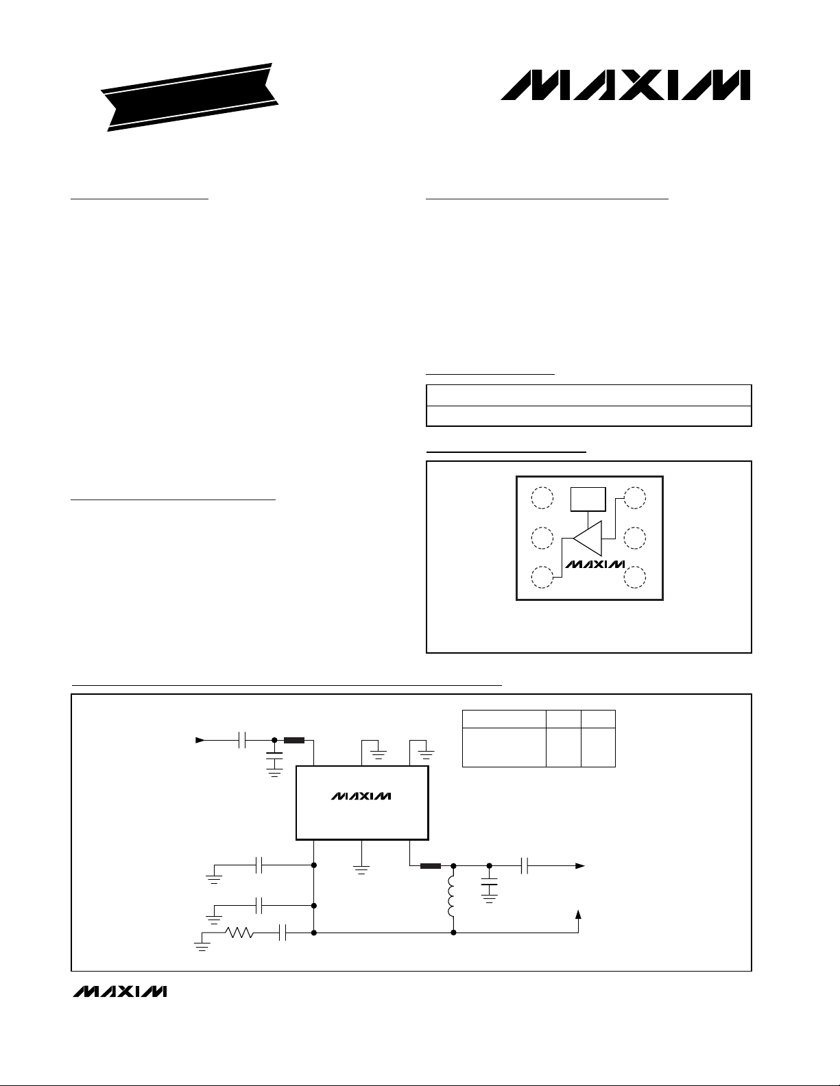
Typical Application Circuit
UCSP is a trademark of Maxim Integrated Products, Inc.
MAX2648EBT -40°C to +85°C2
PART TEMP. RANGE PIN-PACKAGE
✕3 UCSP
V
CC
GND
B2 GND
BIAS
MAX2648
2x3 UCSP
TOP VIEW
(BUMPS ON BOTTOM OF DIE)
A1B1 RFIN
A2
GNDRFOUT
A3B3
C1
100pF
RF INPUT
R2
8.2Ω
C8*
C2
100pF
C3
1000pF
WIDTH = 21 mils
LENGTH = 300 mils**
A1 A2
RFIN GND GND
V
CC
B1
C4
0.01µF
MAX2648
GND RFOUT
B2
A3
WIDTH = 21 mils
B3
LENGTH = 300 mils**
L1
22nH
C7*
1.0pF
0.7pF
RF
OUTPUT
C8*
0.9pF
0.8pF
V
CC
OPERATING BAND
5150MHz TO 5350MHz
5725MHz TO 5825MHz
*THESE ARE ATC 500-SERIES, LOW-LOSS
PORCELAIN 0603 CAPACITORS.
**REFER TO MAX2648 EV KIT DATA SHEET FOR
MORE LAYOUT INFORMATION.
C6
100pF
C7*
Page 2
MAX2648
5GHz to 6GHz Low-Noise Amplifier
in 6-Pin UCSP
2 _______________________________________________________________________________________
ABSOLUTE MAXIMUM RATINGS
DC ELECTRICAL CHARACTERISTICS
(VCC= +2.7V to +3.6V, no RF signals applied, RFIN and RFOUT terminated in 50Ω through a DC-blocking capacitor, RFOUT connected to V
CC
. Typical values for VCC= +3.0V, TA= +25°C, unless otherwise noted.)
Stresses beyond those listed under “Absolute Maximum Ratings” may cause permanent damage to the device. These are stress ratings only, and functional
operation of the device at these or any other conditions beyond those indicated in the operational sections of the specifications is not implied. Exposure to
absolute maximum rating conditions for extended periods may affect device reliability.
Note 1: Limits are guaranteed by design and characterization, and are not production tested.
V
CC
to GND...........................................................-0.3V to +6.0V
RFOUT to GND......................................................-0.3V to +6.0V
RFIN.......................................................................-0.3V to +0.8V
RFIN Power (50Ω source) ..............................................+15dBm
Continuous Power Dissipation
2
✕
3-Bump UCSP (derate 24mW/°C above +70°C) ......500mW
Operating Temperature .......................................-40°C to +85°C
Junction Temperature......................................................+150°C
Storage Temperature.........................................-55°C to +150°C
AC ELECTRICAL CHARACTERISTICS
(MAX2648 evaluation kit, VCC= +3.0V, f
IN
= 5250MHz, PIN= -30dBm, 50Ω system, TA= +25°C. Typical values for V
CC
= +3.0V,
T
A
= +25°C, unless otherwise noted. All limits are guaranteed by design and characterization and are not production tested.)
Note 2: The recommended operating range is 5100MHz to 5850MHz. Operation outside this frequency range is possible but has not
been characterized. The device is matched, characterized, and tested at 5250MHz. For optimum performance at a given
frequency, the input and output ports must be properly matched. See Applications Information section for more information
on matching.
Note 3: Specifications are corrected for board losses (0.4dB at input, 0.4dB at output)
Note 4: Specification is corrected for board losses (0.4dB at input)
Supply Voltage Range V
Supply Current I
PARAMETER SYMBOL CONDITIONS MIN TYP MAX UNITS
CC
CC
TA = +25°C 12.3 15
TA = -40°C to +85°C (Note 1) 18
2.7 3.6 V
mA
Frequency Range f
Power Gain |S21| (Note 3) 16 17.4 dB
Maximum Gain Variation over
Temperature
Input Third Order Intercept IIP3
Noise Figure NF (Note 4) 1.8 2.3 dB
Input Return Loss |S11| -14 dB
Output Return Loss |S22| -14 dB
Reverse Isolation |S12| -31 dB
PARAMETER SYMBOL CONDITIONS MIN TYP MAX UNITS
(Note 2) 5250 MHz
IN
T
= -40°C to +85°C 0.2 1.0 dB
A
Two tones at 5250MHz and 5251MHz,
-30dBm per tone (Note 4)
-4.0 0 dBm
Page 3
MAX2648
5GHz to 6GHz Low-Noise Amplifier
in 6-Pin UCSP
_______________________________________________________________________________________ 3
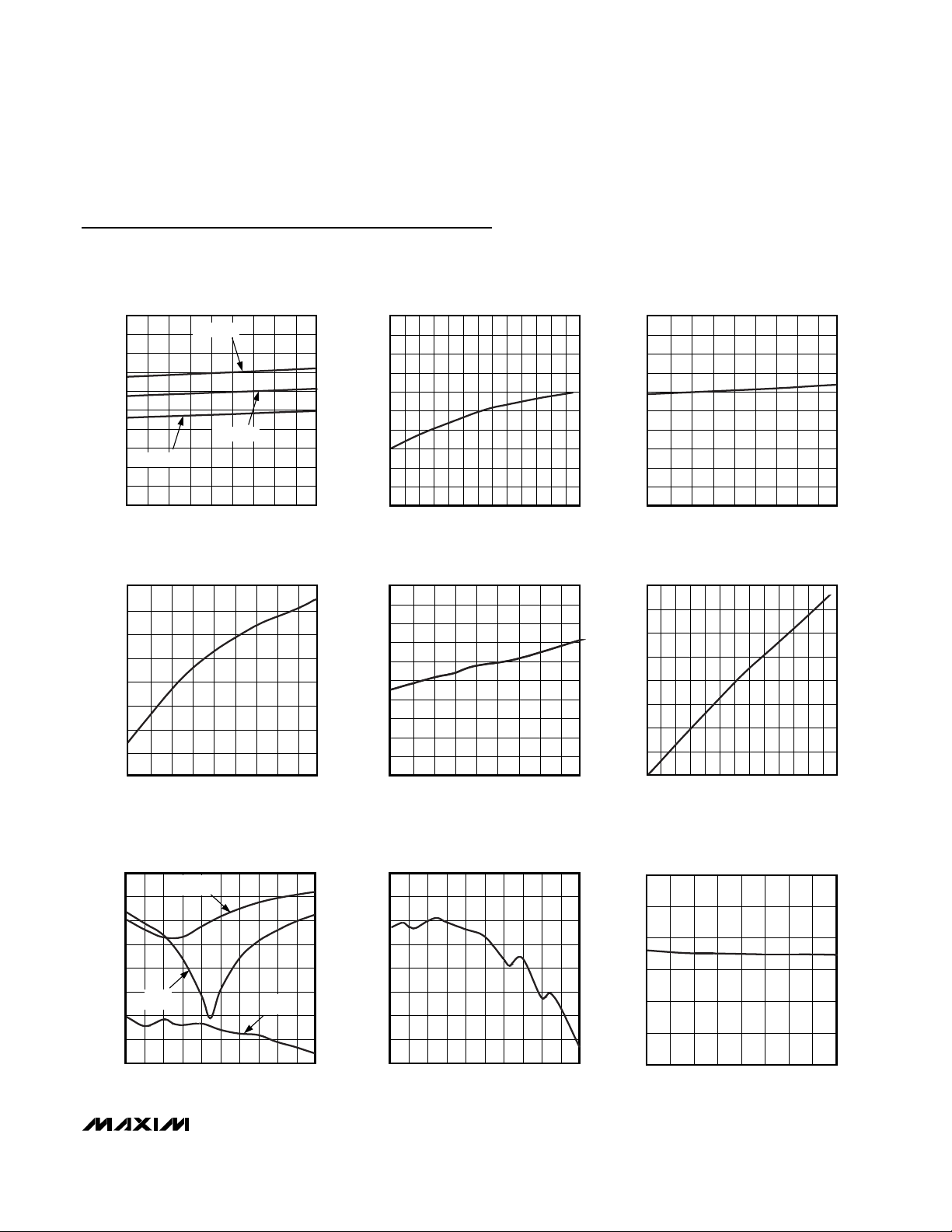
Typical Operating Characteristics
(MAX2648 evaluation kit tuned for 5150MHz to 5350MHz, VCC= +3.0V, fIN= 5250MHz, P
IN
= -30dBm, 50Ω system, TA= +25°C,
unless otherwise noted.)
20
18
16
14
12
10
8
6
SUPPLY CURRENT (mA)
4
2
0
2.7 2.9 3.0 3.12.8 3.2 3.3 3.4 3.5 3.6
7.0
6.8
6.6
6.4
6.2
6.0
5.8
OUTPUT 1dB DOWN POINT (dBm)
5.6
5.4
2.7 2.92.8 3.0 3.1 3.2 3.3 3.4 3.5 3.6
SUPPLY CURRENT
vs. SUPPLY VOLTAGE
TA = +85°C
TA = +25°C
TA = -40°C
SUPPLY VOLTAGE (V)
P(1dB) vs. SUPPLY VOLTAGE
SUPPLY VOLTAGE (V)
18.4
18.2
MAX2648 toc01
18.0
17.8
17.6
17.4
GAIN (dB)
17.2
17.0
16.8
16.6
16.4
-40 -20 -10-30 0 102030405060708090
1.0
0.8
MAX2648 toc04
0.6
0.4
0.2
0
-0.2
-0.4
-0.6
INPUT 3rd-ORDER INTERCEPT (dBm)
-0.8
-1.0
2.7 2.92.8 3.0 3.1 3.2 3.3 3.4 3.5 3.6
GAIN vs. TEMPERATURE
MAX2648 toc02
TEMPERATURE (°C)
IIP3 vs. SUPPLY VOLTAGE
MAX2648 toc05
SUPPLY VOLTAGE (V)
GAIN vs. SUPPLY VOLTAGE
18.2
18.0
17.8
17.6
17.4
17.2
GAIN (dB)
17.0
16.8
16.6
16.4
16.2
2.7 2.92.8 3.0 3.1 3.2 3.3 3.4 3.5 3.6
SUPPLY VOLTAGE (V)
IIP3 vs. TEMPERATURE
2.0
1.5
1.0
0.5
0
-0.5
-1.0
INPUT 3rd-ORDER INTERCEPT (dBm)
-1.5
-2.0
-40 -20 -10-30 01020304050607080
TEMPERATURE (
°C)
MAX2648 toc03
MAX2648 toc06
90
|S11|, |S12|, AND |S22| vs. FREQUENCY
(5250MHz APPLICATION CIRCUIT)
0
-5
-10
-15
-20
-25
MAGNITUDE (dB)
-30
-35
-40
5000 5200 5400 5600 5800 6000
|S22|
|S11|
OPERATING FREQUENCY (MHz)
|S12|
MAX2648 toc07
|S21| vs. FREQUENCY
(5250MHz APPLICATION CIRCUIT)
19
18
17
16
| (dB)
15
21
|S
14
13
12
11
5000 5200 5400 5600 5800 6000
OPERATING FREQUENCY (MHz)
MAX2648 toc08
NOISE FIGURE (dB)
NOISE FIGURE vs. FREQUENCY
(5250MHz APPLICATION CIRCUIT)
3.0
2.5
2.0
1.5
1.0
0.5
0
5150 52005175 5225 5250 5275 5300 5325 5350
OPERATING FREQUENCY (MHz)
MAX2648 toc09
Page 4

Pin Description
MAX2648
5GHz to 6GHz Low-Noise Amplifier
in 6-Pin UCSP
4 _______________________________________________________________________________________
Typical Operating Characteristics (continued)
(MAX2648 evaluation kit tuned for 5150MHz to 5350MHz, VCC= +3.0V, fIN= 5250MHz, P
IN
= -30dBm, 50Ω system, TA= +25°C,
unless otherwise noted.)
-100 1020304050607080 90
NOISE FIGURE vs. TEMPERATURE
(5250MHz APPLICATION CIRCUIT)
MAX2648 toc10
-40 -30-20
0
0.5
1.0
1.5
2.0
2.5
3.0
OPERATING FREQUENCY (MHz)
NOISE FIGURE (dB)
-40
-30
-35
-25
-10
-5
-15
-20
0
5000 5200 5400 5600 5800 6000
|S11|, |S12|, AND |S22| vs. FREQUENCY
(5800MHz APPLICATION CIRCUIT)
MAX2648 toc11
OPERATING FREQUENCY (MHz)
MAGNITUDE (dB)
|S22|
|S11|
|S12|
10
12
11
13
16
17
15
14
18
5000 5200 5400 5600 5800 6000
|S21| vs. FREQUENCY
(5800MHz APPLICATION CIRCUIT)
MAX2648 toc12
OPERATING FREQUENCY (MHz)
|S
21
| (dB)
0
0.5
1.0
1.5
2.0
2.5
3.0
5725 5750 5775 5800 5825
NOISE FIGURE vs. FREQUENCY
(5800MHz APPLICATION CIRCUIT)
MAX2648 toc13
OPERATING FREQUENCY (MHz)
NOISE FIGURE (dB)
PIN NAME FUNCTION
A1 RFIN
A2, A3, B2 GND Ground. Provide a low-inductance connection to the ground plane.
B3 RFOUT
B1 V
CC
Amplifier Input. AC-couple to this pin with a DC-blocking capacitor. External matching network is
required for optimum performance.
Amplifier Output. Provide DC bias to V
(see evaluation kit layout). External matching network is required for optimum performance.
Power-Supply Input. Bypass directly to ground plane at this bump. Additional bypassing may be
necessary for long V
CC
lines.
through an RF choke or a quarter-wave transmission line
CC
Page 5

Detailed Description
The MAX2648 low-noise amplifier offers high gain, high
linearity, and low-noise performance from 5GHz to
6GHz. This LNA also functions as a PA predriver or an
LO buffer. The device has been fully characterized and
tested in the 5.2GHz and 5.8GHz bands.
Applications Information
Optimal gain and noise figure performance requires
input and output matching circuits tuned for the band
of interest. All electrical specifications and typical operating characteristics are measured on the MAX2648
evaluation kit (EV kit), which is tuned for operation in
the 5.2GHz band. Referencing the application circuit,
PC board layout, and components specified in the
MAX2648 EV kit data sheet will reduce evaluation and
design time for 5.2GHz ISM-band system designs. For
applications in other bands, refer to the MAX2648 [S]parameters (Table 1), noise parameters (Table 2), and
comments below to aid design.
Input Matching
The input stage is internally biased, so no external bias
circuitry is required at RFIN. Be sure to AC-couple to
the input.
Since the noise figure of the LNA design is severely
degraded by low-Q matching components, always
design with high-Q wire-wound inductors and low-loss
capacitors. Remember that package parasitics must be
taken into consideration; always use components with
self-resonant frequencies higher than the intended frequency of operation.
Output Matching
The output of the MAX2648 is an open-collector transistor; the DC bias and RF matching network are off-chip
as illustrated in the Typical Application Circuit. Bias the
output stage with VCCthrough an RF choke, leaving as
little pad exposed as possible—any exposed pad here
will act like a small tuning stub and contribute a small,
low-Q, shunt capacitor to the matching network.
If area allows, a better way to supply a bias for narrowband operation is to design in a quarter-wave transmission line. The far side of this high-Z
0
transmission line is
AC-shorted to ground with a radial stub; low-frequency
decoupling is handled by a 1000pF shunt capacitor to
ground nearby. Bias this point through an RF choke,
and decouple the supply with a few µF at the VCCconnection.
Power-Supply Bypassing
Proper power-supply bypassing is essential for highfrequency circuit stability. Place a small value capacitor
as close to the IC as possible to decouple high-frequency noise. Place a larger value capacitor near the
supply to decouple low-frequency noise. Whenever
possible, place the ground-connected side of bypass
capacitors within a few millimeters of the IC’s ground
connections.
Layout Considerations
A properly designed PC board is an essential part of
any RF/microwave circuit. Keep RF signal lines as short
as possible to reduce losses, EMI, and stray inductance. Use multiple separate low-inductance-plated
vias to the ground plane for each ground bump.
The chip-scale package (UCSP) has a bump pitch of
0.5mm (19.7mil) and a bump diameter of 0.3mm
(12mil). Therefore, lay out the solder pad spacing on
0.5mm (19.7mil) centers, and use a pad size of
0.25mm (10mil) and a solder mask opening of 0.33mm
(13mil). Round or square pads are permissible. Refer to
the Maxim application note, Wafer Level Ultra-Chip-
Scale Packaging, for additional detailed information on
UCSP layout and handling.
Chip Information
TRANSISTOR COUNT: 85
MAX2648
5GHz to 6GHz Low-Noise Amplifier
in 6-Pin UCSP
_______________________________________________________________________________________ 5
Page 6

MAX2648
5GHz to 6GHz Low-Noise Amplifier
in 6-Pin UCSP
6 _______________________________________________________________________________________
Table 1. MAX2648 Typical Device [S] Parameters
(TA= +25°C, VCC= +3.0V, ZS= ZL= 50Ω, input and output matching network not included).
FREQUENCY
(MHZ)
100 0.830 -12.7 27.1 22.89 171.3 0.004 72.6 0.984 -6.3
500 0.797 -63.4 25.5 18.88 138.8 0.016 46.6 0.837 -27.0
1000 0.774 -101.4 23.0 14.21 113.6 0.023 28.5 0.706 -40.7
1500 0.774 -126.2 20.6 10.76 94.2 0.025 14.3 0.636 -50.9
2000 0.774 -142.5 18.5 8.483 79.9 0.026 0.2 0.599 -59.5
2500 0.779 -153.2 16.7 6.893 67.6 0.023 -5.9 0.578 -69.9
3000 0.788 -162.4 14.9 5.573 57.8 0.025 -7.8 0.528 -78.8
3500 0.794 -170.0 13.7 4.859 49.8 0.023 -11.8 0.516 -83.0
4000 0.798 -176.3 12.6 4.306 40.7 0.024 -16.5 0.535 -88.0
4500 0.800 178.0 11.6 3.810 32.0 0.024 -27.5 0.553 -95.1
4600 0.803 176.6 11.4 3.733 30.2 0.019 -32.5 0.564 -96.5
4700 0.809 175.5 11.1 3.616 27.6 0.018 -29.4 0.565 -97.8
4800 0.802 174.8 11.0 3.550 26.0 0.022 -39.1 0.575 -99.1
4900 0.803 173.7 10.8 3.481 24.5 0.018 -30.3 0.571 -100.1
5000 0.803 172.9 10.6 3.426 22.4 0.019 -35.8 0.580 -102.4
5100 0.806 172.1 10.5 3.361 21.1 0.018 -34.5 0.587 -103.2
5200 0.801 171.0 10.4 3.324 19.8 0.022 -35.9 0.591 -104.9
5300 0.803 170.6 10.1 3.223 17.1 0.017 -42.7 0.603 -106.6
5400 0.804 169.7 10.0 3.174 15.5 0.017 -29.1 0.600 -107.4
5500 0.809 168.4 9.81 3.094 14.1 0.012 -40.4 0.604 -109.4
5600 0.807 167.7 9.69 3.054 12.2 0.014 -34.7 0.612 -110.8
5700 0.813 167.0 9.46 2.974 10.6 0.014 -44.2 0.622 -112.2
5800 0.818 165.9 9.35 2.937 9.1 0.013 -46.2 0.621 -113.6
5900 0.817 165.7 9.11 2.854 6.5 0.011 -46.4 0.630 -115.6
6000 0.813 164.6 8.97 2.811 5.4 0.010 -44.1 0.637 -117.1
|S
| ∠ S
11
S
11
11
dB |S21| ∠ S
S
21
21
S
12
|S12| ∠ S
S
22
12
|S22| ∠ S
22
Page 7

MAX2648
5GHz to 6GHz Low-Noise Amplifier
in 6-Pin UCSP
_______________________________________________________________________________________ 7
Table 2. MAX2648 Typical Noise Parameters
(TA= +25°C, VCC= +3.0V, data from design simulation.)
FREQUENCY (MHZ) F
5000 1.502
5100 1.528 0.687 159.0 52.2
5200 1.554 0.690 159.8 53.7
5300 1.581 0.692 160.6 55.2
5400 1.613 0.694 161.4 56.8
5500 1.647 0.696 162.2 58.5
5600 1.662 0.700 163.0 59.7
5700 1.672 0.702 163.8 60.8
5800 1.695 0.705 164.6 62.3
5900 1.722 0.707 165.3 63.8
6000 1.750 0.708 166.1 65.3
(dB) |Γ
MIN
0.683 151.8 50.7
| ∠ Γ
OPT
OPT
RN (Ω)
Page 8

MAX2648
5GHz to 6GHz Low-Noise Amplifier
in 6-Pin UCSP
8 _______________________________________________________________________________________
Package Information
6L,UCSP.EPS
 Loading...