

Page 1
General Description
The MAX2642/MAX2643 low-cost, high third-order intercept point (IP3), low-noise amplifiers (LNAs) are
designed for applications in cellular, ISM, SMR, and
PMR systems. They feature a programmable bias,
allowing the IP3 and supply current to be optimized for
specific applications. These LNAs provide up to 0dBm
input IP3 while maintaining a low noise figure of 1.3dB.
The gain for these devices is typically 17dB. The
MAX2642 also features a 13dB attenuation step, which
extends the LNA’s dynamic range. Both devices feature
a shutdown mode that minimizes power consumption.
On-chip output matching saves board space by reducing the number of external components.
The MAX2642/MAX2643 are designed on a low-noise,
advanced silicon-germanium (SiGe) process technology. They operate from a +2.7V to +5.5V single supply
and are available in the ultra-small 6-pin SC70 package.
________________________Applications
800MHz/900MHz Cellular Phones
900MHz Cordless Phones
868MHz/900MHz ISM-Band Wireless Data
PMR/SMR/LMR
Features
♦ Wide Frequency Range: 800MHz to 1000MHz
♦ High Output IP3 and Adjustable
+17dBm at 5.3mA
+7dBm at 2.8mA
♦ Low Noise Figure: 1.3dB at 900MHz
♦ 13dB Attenuation Step (MAX2642)
♦ On-Chip Output Matching
♦ Low-Power Shutdown Mode
♦ +2.7V to +5.5V Single-Supply Operation
♦ Ultra-Small SC70-6 Package
MAX2642/MAX2643
900MHz SiGe, High IP3,
Low-Noise Amplifiers
________________________________________________________________ Maxim Integrated Products 1
Pin Configuration
19-1682; Rev 0; 4/00
For free samples and the latest literature, visit www.maxim-ic.com or phone 1-800-998-8800.
For small orders, phone 1-800-835-8769.
EVALUATION KIT MANUAL
FOLLOWS DATA SHEET
Ordering Information
6 SC70-6
PINPACKAGE
TEMP. RANGE
-40°C to +85°C
MAX2642EXT-T
PART
AAC
TOP
MARK
6 SC70-6-40°C to +85°C
MAX2643EXT-T
AAD
MAX2642
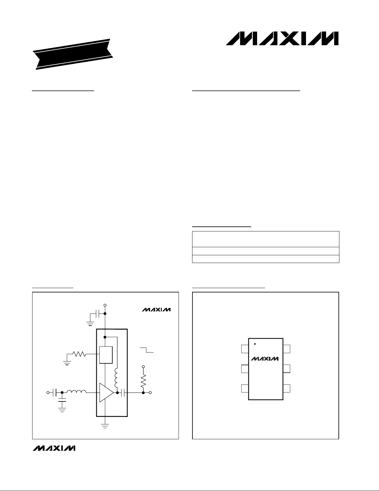
MAX2643
RF
INPUT
GND
RFIN RFOUT
( ) ARE FOR MAX2643.
C1
3.3pF
L1
8.7nH
BIAS
V
CC
V
CC
47pF
R
BIAS
510Ω
RF
OUTPUT
33k
(10k)
LOW GAIN
(ENABLE)
HIGH GAIN
(SHUTDOWN)
BIAS
Typical Operating Circuit
TOP VIEW
16RFOUT
BIAS
GND
RFIN
MAX2642
2
MAX2643
34
5 GND
V
CC
SC70-6
Page 2
MAX2642/MAX2643
900MHz SiGe, High IP3,
Low-Noise Amplifiers
2 _______________________________________________________________________________________
ABSOLUTE MAXIMUM RATINGS
DC ELECTRICAL CHARACTERISTICS—MAX2642
(VCC= +2.7V to +5.5V, TA= -40°C to +85°C, no RF signal applied, RFIN and RFOUT are AC-coupled and terminated to 50Ω, highgain mode. Typical values are at V
CC
= 3.0V, TA= +25°C, unless otherwise noted.) (Notes 1, 2, 3)
DC ELECTRICAL CHARACTERISTICS—MAX2643
(VCC= +2.7V to +5.5V, TA= -40°C to +85°C, no RF signal applied, RFIN and RFOUT are AC-coupled and terminated to 50Ω. Typical
values are at V
CC
= 3.0V, TA= +25°C, unless otherwise noted.) (Notes 1, 8, 9)
Stresses beyond those listed under “Absolute Maximum Ratings” may cause permanent damage to the device. These are stress ratings only, and functional
operation of the device at these or any other conditions beyond those indicated in the operational sections of the specifications is not implied. Exposure to
absolute maximum rating conditions for extended periods may affect device reliability.
VCCto GND..............................................................-0.3V to +6V
RFOUT to GND...........................................-0.3V to (V
CC
+ 0.3V)
RFIN to GND ..................................................................0 to 0.9V
RFIN Power (50Ω source) ................................................+5dBm
BIAS to GND ................................................................0 to +0.3V
Operating Temperature Range ...........................-40°C to +85°C
Maximum Junction Temperature .....................................+150°C
Continuous Power Dissipation (T
A
= +70°C)
SC70-6 (derate 3.1mW/°C above +70°C)...................245mW
Storage Temperature Range .............................-65°C to +150°C
Lead Temperature (soldering, 10s) .................................+300°C
PARAMETER CONDITIONS
MIN
TYP
MAX
UNITS
Supply Voltage 2.7 5.5 V
High-gain mode, R
BIAS
= 510Ω, TA = +25°C 5.3 6.7
R
BIAS
= 510Ω, TA = -40°C to +85°C 7.5
R
BIAS
= 806Ω 3.6
R
BIAS
= 1.1kΩ 2.8
Operating Supply Current
Low-gain mode, R
BIAS
= 510Ω, TA = 25°C 5.9
mA
Shutdown Supply Current BIAS = unconnected (see Applications Information) 0.2 mA
High-gain mode (Note 4) 0.6
Gain Control Voltage Input
Low-gain mode (Note 5) 2.0
V
High-gain mode (Note 6) -10 0
Gain Control Input Current
Low-gain mode (Note 7) 0 50
µA
Supply Voltage 2.7 5.5 V
Operating Supply Current
Shutdown Supply Current Shutdown mode (see Applications Information) 0.2 10 µA
Shutdown Control Input Voltage
Shutdown Control Input Current
PARAMETER CONDITIONS MIN TYP MAX UNITS
R
= 510Ω, TA = +25°C 5.1 6.5
BIAS
R
= 510Ω, TA = -40°C to +85°C 7.3
BIAS
R
= 806Ω 3.4
BIAS
R
= 1.1kΩ 2.6
BIAS
Normal operation (Note 10) 2.0
Shutdown mode (Note 11) 0.6
Normal operation (Note 7) 0 10
Shutdown mode (Note 6) -5 5
mA
V
µA
Page 3
MAX2642/MAX2643
900MHz SiGe, High IP3,
Low-Noise Amplifiers
_______________________________________________________________________________________ 3
AC ELECTRICAL CHARACTERISTICS
(MAX2642/MAX2643 EV kits, P
RFIN
= -30dBm, f
RFIN
= 900MHz, input and output are terminated to 50Ω, VCC= +3.0V, TA= +25°C,
R
BIAS
= 510Ω, unless otherwise noted.) (Note 12)
PARAMETER CONDITIONS
MIN
TYP
MAX
UNITS
Operating Frequency Range (Note 13)
MHz
Gain (Note 14) TA = +25°C
19 dB
Gain Variation Over Temperature
TA = -40°C to +85°C
dB
Attenuation Step MAX2642 only 13 dB
R
BIAS
= 510Ω 0
R
BIAS
= 806Ω -5
Input Third-Order Intercept Point
(Note 15)
R
BIAS
= 1.1kΩ -10
dBm
-18
Input 1dB Compression Point
MAX2642, low-gain mode -17
dBm
1.6
Noise Figure (Note 16)
MAX2642, low-gain mode 4.3
dB
-10 -12
Input Return Loss
MAX2642, low-gain mode -10 -18
dB
-10 -14
Output Return Loss
MAX2642, low-gain mode -10 -11
dB
-20 -26
Reverse Isolation
MAX2642, low-gain mode -10 -17
dB
Gain-Step Response Time MAX2642 5 10 µs
MAX2643 6 10
Shutdown Response Time
MAX2642, through series switch at BIAS 12
µs
Note 1: Devices are production tested at TA= +25°C. Minimum and maximum values are guaranteed by design and characterization
over temperature and supply voltage.
Note 2: High-gain mode is set for the MAX2642 by connecting RFOUT to GND through a 33kΩ resistor.
Note 3: Low-gain mode is applicable only to the MAX2642 and is set by connecting RFOUT to V
CC
through a 33kΩ resistor.
Note 4: Maximum DC voltage through a 33kΩ resistor that sets the MAX2642 to operate in high-gain mode.
Note 5: Minimum DC voltage through a 33kΩ resistor that sets the MAX2642 to operate in low-gain mode.
Note 6: DC current required when RFOUT is connected to GND through a 33kΩ resistor (MAX2642) and 10kΩ resistor (MAX2643).
Note 7: DC current required when RFOUT is connected to V
CC
through a 33kΩ resistor (MAX2642) and 10kΩ resistor (MAX2643).
Note 8: Normal operation is set for the MAX2643 by connecting RFOUT to V
CC
through a 10kΩ resistor.
Note 9: Shutdown is set for the MAX2643 by connecting RFOUT to GND through a 10kΩ resistor.
Note 10: Minimum DC voltage through a 10kΩ resistor that sets the MAX2643 to operate in normal mode.
Note 11: Maximum DC voltage through a 10kΩ resistor that sets the MAX2643 to operate in shutdown mode.
Note 12: Min/Max limits are guaranteed by design and characterization, except gain is production tested at T
A
= +25°C.
Note 13: The part has been characterized at the specified frequency range. Operation outside this range is possible but not guar-
anteed.
Note 14: Devices are production tested at T
A
= +25°C.
Note 15: Measured with two input tones, f
1
= 895MHz and f2= 905MHz, both at -30dBm per tone.
Note 16: Excludes PC board losses (0.25dB typical at the input of the MAX2642/MAX2643 EV kit).
800 1000
14.5 16.7
±0.35 ±0.75
1.35
Page 4
MAX2642/MAX2643
900MHz SiGe, High IP3,
Low-Noise Amplifiers
4 _______________________________________________________________________________________
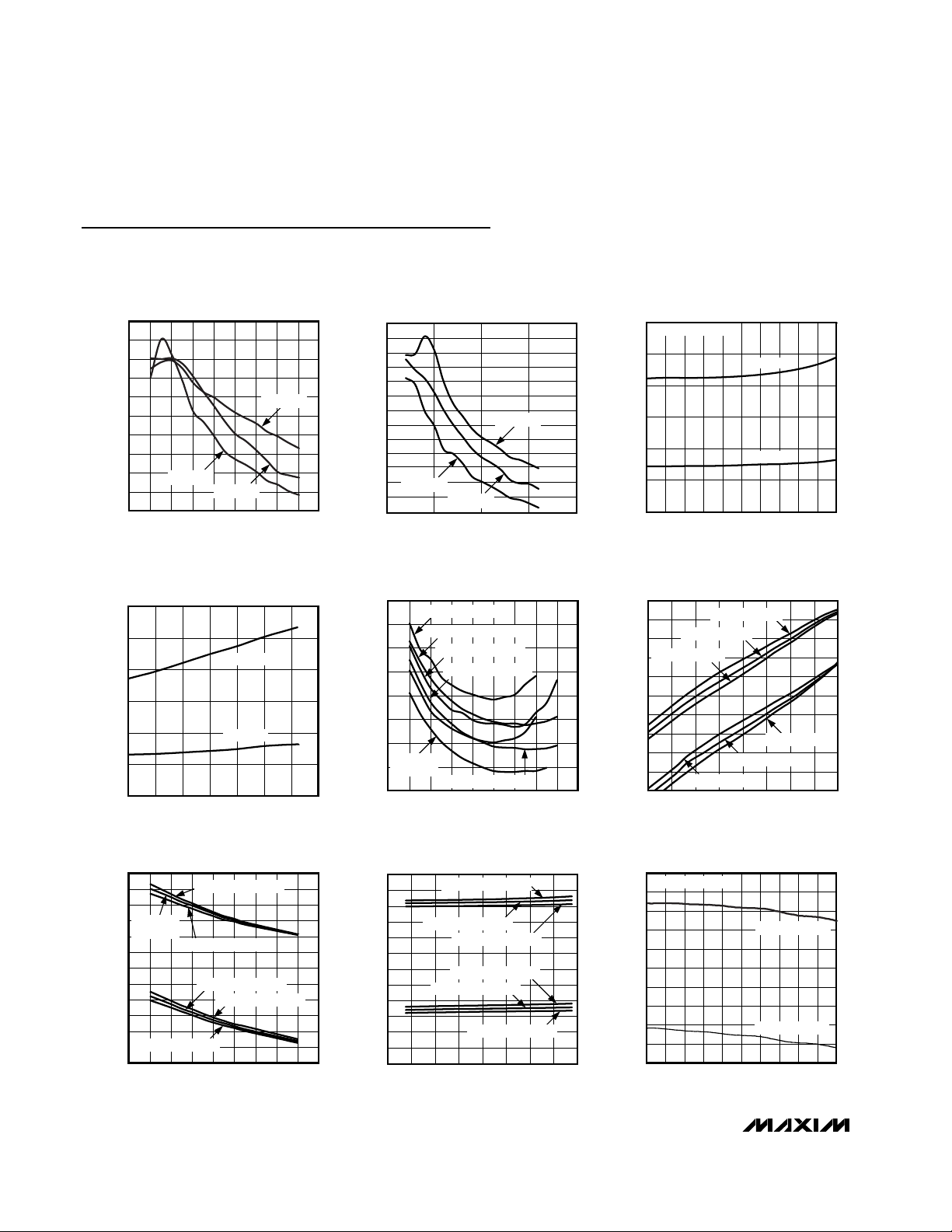
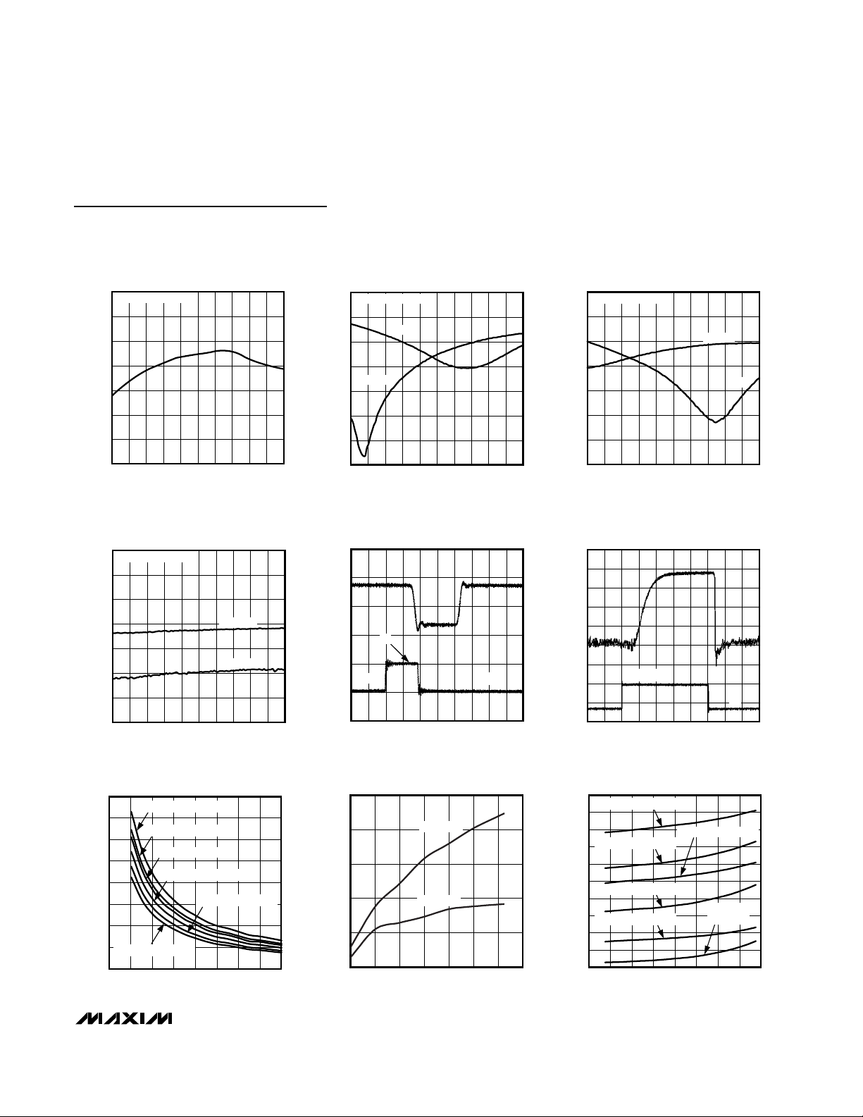
Typical Operating Characteristics
(MAX2642/MAX2643 EV kits, VCC= +3.0V, P
RFIN
= -30dBm, input and output are terminated to 50Ω, f
RFIN
= 900MHz, R
BIAS
=
510Ω, high-gain mode (low-gain mode is applicable only to the MAX2642), T
A
= +25°C, unless otherwise noted.)
-15
-11
-13
-7
-9
-3
-5
-1
3
1
5
0 400 600 800200 1000 1200 1400 1600 1800
INPUT THIRD-ORDER INTERCEPT
vs. R
BIAS
(HIGH GAIN)
MAX2642/43-01
R
BIAS
(Ω)
INPUT IP3 (dBm)
TA = +85°C
TA = +25°C
TA = -40°C
-15
-1
-3
3
1
7
5
9
11
MAX2642
INPUT THIRD-ORDER INTERCEPT
vs. R
BIAS
(LOW GAIN)
MAX2642/43-02
R
BIAS
(Ω)
INPUT IP3 (dBm)
0 500 1000 1500 2000
-5
-7
-9
-11
-13
TA = +85°C
TA = +25°C
TA = -40°C
0
3
2
1
4
5
6
800 880860820 840 900 920 940 960 980 1000
NOISE FIGURE vs. FREQUENCY
MAX2642/43-03
FREQUENCY (MHz)
NOISE FIGURE (dB)
LOW GAIN
HIGH GAIN
MATCHED AT 900MHz
0
1
2
4
3
5
6
-40 -20 0 20 40 60 80 100
NOISE FIGURE vs. TEMPERATURE
MAX2642/43-04
NOISE FIGURE (dB)
LOW GAIN
HIGH GAIN
-24
-20
-22
-14
-16
-18
-10
-12
-8
0 600 800200 400 1000 1200 1400 1600 1800
P1dB vs. R
BIAS
MAX2642/43-05
R
BIAS
(Ω)
P1dB (dBm)
TA = -40°C,
HIGH GAIN
TA = +85°C, HIGH GAIN
TA = -40°C, LOW GAIN
TA = +85°C, LOW GAIN
TA = +25°C, LOW GAIN
TA = +25°C, HIGH GAIN
-28
-20
-24
-12
-16
-4
-8
0
8
4
12
-30 -22 -18-26 -14 -10 -6 -2 2
OUTPUT POWER vs. INPUT POWER
MAX2642/43-06
PIN (dBm)
P
OUT
(dBm)
510Ω, HIGH GAIN
1.1kΩ, LOW GAIN
510Ω, LOW GAIN
806Ω, LOW GAIN
806Ω, HIGH GAIN
1.1kΩ, HIGH GAIN
0
4
2
8
6
12
10
14
18
16
20
0 400 600 800200 1000 1200 1400 1600 1800
GAIN vs. R
BIAS
MAX2642/43-07
R
BIAS
(Ω)
GAIN (dB)
-2
-4
TA = +85°C, HIGH GAIN
TA = -40°C, HIGH GAIN
TA = -40°C, LOW GAIN
TA = +85°C, LOW GAIN
TA = +25°C,
HIGH GAIN
TA = +25°C, LOW GAIN
4
10
8
6
12
14
18
16
20
2.4 2.8 3.2 3.6 4.0 4.4 4.8 5.2 5.6
GAIN vs. SUPPLY VOLTAGE
MAX2642/43-08
VCC (V)
GAIN (dB)
2
0
-2
-4
TA = +85°C, HIGH GAIN
TA = -40°C, HIGH GAIN
TA = -40°C, LOW GAIN
TA = +85°C, LOW GAIN
TA = +25°C, LOW GAIN
TA = +25°C, HIGH GAIN
0
4
2
8
6
12
10
14
18
16
20
800 840 860 880820 900 920 940 980960 1000
GAIN vs. FREQUENCY
MAX2642/43-09
FREQUENCY (MHz)
GAIN (dB)
MATCHED AT 900MHz
LOW-GAIN MODE
HIGH-GAIN MODE
Page 5
MAX2642/MAX2643
900MHz SiGe, High IP3,
Low-Noise Amplifiers
_______________________________________________________________________________________ 5
Typical Operating Characteristics (continued)
(MAX2642/MAX2643 EV kits, VCC= +3.0V, P
RFIN
= -30dBm, input and output are terminated to 50Ω, f
RFIN
= 900MHz, R
BIAS
=
510Ω, high-gain mode (low-gain mode is applicable only to the MAX2642), T
A
= +25°C, unless otherwise noted.)
MAX2642
ATTENUATION STEP vs. FREQUENCY
14.0
MATCHED AT 900MHz
13.8
13.6
13.4
13.2
13.0
ATTENUATION STEP (dB)
12.8
12.6
800 880840 920 960820 900860 940 980 1000
FREQUENCY (MHz)
MAX2642/43-10
REVERSE ISOLATION vs. FREQUENCY
0
MATCHED AT 900MHz
-5
-10
-15
-20
RETURN LOSS (dB)
-25
-30
-35
800 880840 920 960820 900860 940 980 1000
FREQUENCY (MHz)
16
14
12
10
SUPPLY CURRENT (mA)
SUPPLY CURRENT vs. R
TA = +85°C, LOW GAIN
TA = +85°C, HIGH GAIN
TA = +25°C, LOW GAIN
8
6
4
2
TA = -40°C, HIGH GAIN
0
0 400 600200 800 1000 1200 1400 1600
TA = +25°C, HIGH GAIN
LOW GAIN
HIGH GAIN
TA = -40°C, LOW GAIN
R
(Ω)
BIAS
BIAS
MAX2642/43-13
MAX2642/43-16
RETURN LOSS vs. FREQUENCY
(HIGH GAIN)
0
MATCHED AT 900MHz
-5
-10
-15
-20
-25
ATTENUATION STEP (dB)
-30
-35
800 880840 920 960820 900860 940 980 1000
INPUT
OUTPUT
FREQUENCY (MHz)
MAX2642
HIGH/LOW-GAIN SWITCH
CHARACTERISTICS
0
-10
-20
-30
-40
OUTPUT POWER (dBm)
-50
-60
3V
0V
TIME (400ns/div)
SHUTDOWN CURRENT
vs. TEMPERATURE
10
1
0.1
0.01
SHUTDOWN CURRENT (µA)
0.001
0.0001
-40 -20 0 20 40 60 80 100
VCC = 5.5V
VCC = 3.0V
TEMPERATURE (°C)
RETURN LOSS vs. FREQUENCY
0
MATCHED AT 900MHz
-5
MAX2642/43-11
-10
-15
-20
RETURN LOSS (dB)
-25
-30
-35
800 880840 920 960820 900860 940 980 1000
SHUTDOWN CHARACTERISTICS
0
-10
MAX2642/43-14
-20
-30
-40
-50
-60
V
RFOUT
OUTPUT POWER (dBm)
-70
-80
-90
V
vs. SUPPLY VOLTAGE
8.0
TA = +85°C, LOW GAIN
7.6
MAX2642/43-17
7.2
TA = +85°C, HIGH GAIN
6.8
6.4
6.0
TA = +25°C, HIGH GAIN
5.6
5.2
SUPPLY VOLTAGE (mA)
TA = -40°C, LOW GAIN
4.8
4.4
4.0
2.4 3.2 3.62.8 4.0 4.4 4.8 5.2 5.6
MAX2642
(LOW GAIN)
FREQUENCY (MHz)
MAX2643
RFOUT
TIME (4µs/div)
3V
SUPPLY CURRENT
TA = +25°C, LOW GAIN
SUPPLY VOLTAGE (V)
OUTPUT
INPUT
TA = -40°C,
HIGH GAIN
0V
MAX2642/43-12
MAX2642/43-15
MAX2642/43-18
Page 6

MAX2642/MAX2643
900MHz SiGe, High IP3,
Low-Noise Amplifiers
6 _______________________________________________________________________________________
Pin Description
PIN NAME FUNCTION
1 BIAS
Resistor Bias Control. Connect a resistor, R
BIAS
, from BIAS to ground. R
BIAS
sets IP3 and supply
current (see Applications Information). The current through this pin is approximately 50mV divided
by R
BIAS
.
2, 5 GND Ground. For optimum performance, provide a low-inductance connection to the ground plane.
3 RFIN
Amplifier Input. AC-couple to this pin with a DC-blocking capacitor. External matching network is
required for optimum performance.
4V
CC
Supply Voltage. Bypass with a 47pF capacitor directly to ground at the supply pin. Additional
bypassing may be necessary for long V
CC
lines.
6 RFOUT Amplifier Output. Internally matched to 50Ω. DC bias on this pin selects gain mode (MAX2642) or
shutdown mode (MAX2643) (see Applications Information).
Applications Information
Input Matching
Input matching is required for optimum performance.
The MAX2642/MAX2643 require a simple LC matching
network, as shown in the Typical Operating Circuit. To
further reduce cost and external component count,
replace the external inductor with a microstrip transmission line. The Typical Operating Circuit shows the recommended input-matching networks for the MAX2642/
MAX2643 at 900MHz. These values are optimized for
best simultaneous gain, noise figure, and return-loss
performance. To aid in the design of the matching network for other frequencies, Tables 1–6 list typical
device S-parameters for various biases, and Tables 7,
8, and 9 list typical device noise parameters.
Attenuation Step (MAX2642)
The MAX2642’s DC bias voltage at RFOUT serves as
an attenuation step input. When the DC voltage at
RFOUT through a 33kΩ resistor is less than +0.6V, the
device is in high-gain mode; if the DC voltage is greater
than +2.0V, the device is in low-gain mode. A standard
logic output can be applied as shown in the Typical
Operation Circuit. If no bias is applied, the device is in
high-gain mode.
Shutdown
For the MAX2643, the recommended shutdown method
is to set the DC voltage at the RFOUT pin in a manner
similar to the MAX2642’s attenuation step. That is, when
the DC voltage at RFOUT is below +0.6V, the device is
shut down; if the DC voltage is greater than +2.0V, the
device is enabled.
For the MAX2642, shutdown is achieved by leaving
BIAS unconnected. Figure 1 shows the suggested
shutdown methods. Avoid capacitance at the BIAS pin
by connecting the bias resistor from BIAS to the switch.
Table 10 summarizes the operational modes.
Layout Issues
A properly designed PC board is essential to any
RF/microwave circuit. Use controlled impedance lines
on all high-frequency inputs and outputs. Bypass with
decoupling capacitors located close to the device V
CC
pin. For long VCClines, it may be necessary to add
additional decoupling capacitors. These additional
capacitors can be located farther away from the device
package. Proper grounding of the GND pins is essential. If the PC board uses a topside RF ground, connect
it directly to all GND pins. For a board where the
ground plane is not on the component layer, the best
technique is to connect the GND pins to the board with
a plated through-hole located close to the package.
Page 7

MAX2642/MAX2643
900MHz SiGe, High IP3,
Low-Noise Amplifiers
_______________________________________________________________________________________ 7
Table 1. MAX2642/MAX2643 Typical Scattering Parameters
(R
BIAS
= 510Ω, high-gain mode, VCC= +3.0V, TA= +25°C.)
FREQ
(MHz)
S11 MAG
S11 PHASE
S21 MAG
S21 PHASE
S12 MAG
S12 PHASE
S22 MAG
S22 PHASE
(DEGREES)
500
-69.5831
-119.18
-74.01422
600
-83.7622
-136.451
-98.95091
700
-97.3356
-161.126 0.02988
-125.1027
800 0.73798 -108.682
-142.0387
820
-110.578 5.286
132.505
-141.9486
840
-112.499
-139.9869
860
-114.276
-133.8375
880
-115.973
-121.3533
900
-117.585
128.075
-102.3972
920
-119.117
0.06007
-81.32555
940
-120.995
0.04301
-62.51575
960 0.68522 -122.642
-50.8638
980
-124.345
0.04524
-44.30662
1000
-126.035
-40.69565
1100
-134.195 4.29304
-34.00603
1200
-141.558
-32.62157
1300
-147.886
103.583
-33.12784
1400
-153.992
-36.62076
1500
-158.21
-40.68451
0.832641
0.825168
0.785389
0.728099
0.718704
0.711335
0.705742
0.699509
0.695913
0.690406
0.681722
0.675328
0.657582
0.635999
0.616881
0.602418
0.587409
(DEGREES)
2.390806
3.836967
4.983279
5.320575 174.5337 0.036197 134.8794 0.215462
5.241719 166.3987 0.037266 129.1671 0.135415
5.185213 162.4763 0.039143 128.0447 0.100779
5.118265 158.9238 0.039563 128.4158 0.076864
5.050356 155.6292 0.042586
4.973824 152.4338 0.041805 126.9362
4.897571 149.4286
4.826106 146.6999 0.046528 122.0997 0.077374
4.735407 143.8275
4.650673 141.4611 0.046036 120.1779 0.103072
3.998256 121.5475 0.061434 109.6365 0.198686
3.777511 113.2893 0.066092
3.547677 105.6808 0.075756 99.08275 0.283245
3.338385 97.62961 0.076491 92.84421 0.326279
(DEGREES)
0.010763 166.6047 0.878515
0.019608 167.8741 0.731997
170.3323 0.037193
130.7613 0.053825 116.4169 0.156945
(DEGREES)
148.5203 0.481344
0.171633
0.062918
122.9564 0.065287
121.0474 0.090494
0.240437
Page 8

MAX2642/MAX2643
900MHz SiGe, High IP3,
Low-Noise Amplifiers
8 _______________________________________________________________________________________
Table 2. MAX2642/MAX2643 Typical Scattering Parameters
(R
BIAS
= 806Ω, high-gain mode, VCC= +3.0V, TA= +25°C.)
FREQ
(MHz)
S11 MAG
S11 PHASE
(DEGREES)
S21 MAG
S21 PHASE
(DEGREES)
S12 MAG
S12 PHASE
(DEGREES)
S22 MAG
S22 PHASE
(DEGREES)
500
-67.5629
-115.899
600
-80.7084
-132.446
165.374
700
-94.1329
-157.426
0.49107
800
-104.428
820
-106.343
840 0.759 -108.042
169.298
860 0.7495 -109.928
880
-111.683
161.548 0.04118
900
-113.369
0.04194
920
-115.127
940
-116.951
960
-118.584
980
-120.313 3.83867
118.109
1000
-121.959 3.777
119.036
1100
-129.341
1200 0.67035 -136.703 3.27255
1300
-143.014 3.09574
0.26965
1400
-148.565
97.9223
1500
-153.536
0.865705
0.853946
0.820187
0.775557
0.765138
0.741722
0.736069
0.728957
0.724118
0.719676
0.714506
0.709103
0.691292
0.650556
0.635363
0.616202
1.788918
2.926709
3.884537
4.237314 177.9528 0.036728 130.1148 0.216415 -153.3392
4.226094 173.3886 0.038253 129.5942 0.166772 -157.7809
4.214913
4.182436 165.3457 0.040084 127.3742 0.082263 -160.9349
4.134814
4.085018 157.8688
4.032105 154.6118 0.044642 123.3553 0.021369 -38.41852
3.965561 151.3371 0.044574 121.8034 0.043243 -17.90431
3.903364 148.3141 0.044792 120.7695 0.066898 -14.20027
3.483283 131.8578 0.054775 114.7347 0.169693 -18.18657
2.934971 105.3286 0.075142
2.756155 96.43876 0.074664 92.88747 0.360706 -35.70454
0.009763 164.6001 0.880237 -73.81893
0.021656
0.029766 148.5047
0.038842 128.7876 0.121201 -160.7175
127.2791 0.045314 -158.0615
125.3719 0.016624 -133.0426
145.3527 0.045551
142.7001 0.046434
121.9156 0.061407 108.2008 0.220689 -21.72272
113.1691 0.064829 103.5856
0.739354 -99.52715
-128.1454
0.084163 -12.76007
0.102269 -13.88384
-24.86245
0.315264 -30.21604
Page 9
MAX2642/MAX2643
900MHz SiGe, High IP3,
Low-Noise Amplifiers
_______________________________________________________________________________________ 9
Table 3. MAX2642/MAX2643 Typical Scattering Parameters
(R
BIAS
= 1.1kΩ, high-gain mode, VCC= +3.0V, TA= +25°C.)
FREQ
(MHz)
S11 MAG
S11 PHASE
S21 MAG
S11 PHASE
S12 MAG
S12 PHASE
S22 MAG
S22 PHASE
(DEGREES)
500
-66.0475
-114.652
-73.97408
600 0.86813 -79.0081
-131.281 0.01977
-100.0799
700
-91.9431
-155.869
-129.8978
800
-102.384
-160.5161
820
-104.098
-166.8809
840
-105.921
-173.2415
860
-107.766
165.871 0.04004
178.6352
880
-109.461
167.1237
900
-111.254
128.5957
920
-113.148
48.71712
940
-114.988 3.36768
0.04661 18.5372
960
-116.709
10.02515
980
-118.379
118.374
4.197083
1000
-119.87
-0.293905
1100
-127.286
-10.46082
1200
-134.781
-16.81635
1300
-141.275
-21.34393
1400
-146.685
-27.6725
1500
-152.12
-33.81158
0.878512
0.834311
0.793611
0.783644
0.774329
0.767016
0.762463
0.753622
0.748921
0.743011
0.737437
0.733572
0.729122
0.710864
0.688941
0.668471
0.655478
0.638124
(DEGREES)
1.445864
2.398259
3.218232
3.544617 179.1002 0.038594 131.9641 0.223248
3.563583 174.4488 0.040112 131.6111 0.173175
3.546937 170.1934 0.038383 128.1902 0.126351
3.529998
3.500193 161.8438 0.041375 124.4402 0.049822
3.463616 158.0655 0.043587 123.8527 0.020398
3.419726 154.6982 0.043975 123.9237 0.024778
3.309045 148.0373 0.044426 118.9012 0.070736
3.261195 145.4087 0.046581
3.203007 142.5148 0.048343 116.9249 0.110062
2.970843 130.8328 0.055616 115.1579 0.183756
2.789044 120.5809 0.061803 105.9973 0.238134
2.637086 111.4044 0.065281 100.6171 0.289607
2.491515 103.3737 0.073887 96.84646 0.335752
2.352013 94.07729 0.077901 90.34502 0.381179
(DEGREES)
0.011049 175.9688 0.882121
0.033312 149.3926 0.502282
151.2749 0.045614 121.0385
(DEGREES)
166.0087 0.745577
126.4807 0.086328
0.092621
Page 10

MAX2642/MAX2643
900MHz SiGe, High IP3,
Low-Noise Amplifiers
10 ______________________________________________________________________________________
Table 4. MAX2642 Typical Scattering Parameters
(R
BIAS
= 510Ω, low-gain mode, VCC= +3.0V, TA= +25°C.)
FREQ
(MHz)
S11 MAG
S11 PHASE
S21 MAG
S21 PHASE
S12 MAG
S12 PHASE
S22 MAG
S22 PHASE
(DEGREES)
500
-68.0641
-175.019
0.87996 -73.8882
600 0.75734 -84.3042
-146.702
0.71413 -98.6736
700
-98.422
-174.61
-121.361
800
-107.497
-127.267
820
-108.596
152.644
-123.451
840
-109.794
-116.955
860
-110.754
-107.057
880
-111.776 1.22394
-93.617
900
-112.739
-81.5882
920
-113.712
86.9857
-70.2192
940
-114.834
128.909
-61.7886
960
-115.806
-55.1485
980
-116.828
-52.3827
1000
-117.975
0.12743
-48.4917
1100
-124.002
-43.8143
1200 0.6066 -129.873
99.7348
-43.9084
1300
-136.272
-46.8967
1400
-142.195
85.7905
0.33692 -51.7496
1500
-147.446
-56.7658
(DEGREES)
0.757279
0.696969
0.626874
0.616023
0.608751
0.600617
0.596488
0.593722
0.590101
0.588409
0.589625
0.588079
0.588646
0.597562
0.617079
0.628195
0.640304
0.186886
0.715305
1.140352
1.272844 157.4571 0.115242 103.1406 0.201112
1.267541
1.258504 148.0772 0.117601 97.74948 0.137812
1.242296 143.7583 0.119312 95.48379 0.118557
1.203776 135.9799 0.124196 90.21815 0.103446
1.181885 132.3471 0.125203
1.156787
1.129734 125.6671 0.127369 82.07469 0.129083
1.102653 122.5478 0.127952 80.98836 0.140436
1.074686 119.9067
0.952505 108.5103 0.134236 72.42102 0.206216
0.852237
0.778154 92.06538 0.142609 58.40858 0.295689
0.718399
0.656535 78.77735 0.149518 46.71009 0.374046
(DEGREES)
0.032297 163.9787
0.066113 148.5775
0.099941 124.8504 0.449346
0.116521 100.3007 0.165909
139.7228 0.122318 93.07481 0.106845
0.126462 84.27329 0.116508
0.138354 65.08001 0.252003
0.153771 52.64912
(DEGREES)
0.108109
79.48192 0.151608
Page 11

MAX2642/MAX2643
900MHz SiGe, High IP3,
Low-Noise Amplifiers
______________________________________________________________________________________ 11
Table 5. MAX2642 Typical Scattering Parameters
(R
BIAS
= 806Ω, low-gain mode, VCC= +3.0V, TA= +25°C.)
FREQ
(MHz)
S11 PHASE
S21 PHASE
S12 PHASE
S22 PHASE
(DEGREES)
500
-67.1945
-174.341
161.583 0.88084
-73.57176
600
-81.9096
-143.848
-99.08562
700
-95.21
-171.542
-124.5513
800
-103.586
-136.0146
820
-104.763
-133.6185
840
-106.009
-125.307
860
-107.125
-112.6535
880
-108.175
-92.15154
900
-109.302
0.0738
-70.16955
920
-110.728
-54.68721
940
-111.842
-46.62902
960
-113.103 0.90238
0.12394
-40.63098
980
-114.555
-38.28101
1000
-115.739
-35.93101
1100
-121.754
109.613
-35.70716
1200
-128.101
-37.84105
1300 0.65637 -134.578
93.1824
-41.83445
1400
-139.905
51.5965 0.34549
-46.96146
1500
-145.73 0.53929
-52.44192
S11 MAG
0.800327
0.793203
0.736656
0.676741
0.666567
0.660377
0.651791
0.651106
0.643048
0.643064
0.641773
0.640079
0.641175
0.641025
0.647379
0.651053
0.662035
0.665418
(DEGREES)
S21 MAG
0.142134
0.543072
0.885917
1.005172 159.8524 0.114894 101.0446 0.183694
1.005053 154.9507 0.115809 97.08399 0.143872
0.998032 150.1753 0.118042 94.72314 0.109486
0.990225 145.7345 0.118937 91.64486 0.085206
0.978178 141.4141 0.121575 89.19647 0.071836
0.961026 137.4554 0.120654 86.75212
0.942776 133.7632 0.123645 83.74419 0.084769
0.923851 130.1361 0.123333 80.71953 0.098778
0.879907 123.7699 0.123001 76.38534 0.132356
0.857382 120.9598 0.122316 74.64619 0.145883
0.760331
0.685309 100.4887 0.131962 62.04964 0.260554
0.623917
0.582929 86.98415 0.142149
(DEGREES)
126.9098
79.50793 0.138295 45.87176 0.382116
S12 MAG
0.034805
0.067027 146.5234 0.719105
0.101665 122.4962 0.449898
0.127968 68.72507 0.209937
0.132337 56.01043 0.303628
(DEGREES)
78.64308 0.117484
S22 MAG
Page 12

MAX2642/MAX2643
900MHz SiGe, High IP3,
Low-Noise Amplifiers
12 ______________________________________________________________________________________
Table 6. MAX2642 Typical Scattering Parameters
(R
BIAS
= 1.1Ω, low-gain mode, VCC= +3.0V, TA= +25°C.)
FREQ
(MHz)
S11 MAG
S11 PHASE
S21 MAG
S21 PHASE
S12 MAG
S12 PHASE
S22 MAG
S22 PHASE
(DEGREES)
500
-66.5029
-174.275 0.03386
-73.74798
600
-80.314
-143.103
-99.6653
700
-93.0574 0.72921 -170.915 0.0999
-126.0206
800
-101.403
-141.9359
820
-102.693
-140.7761
840
-103.96
150.551
-136.1769
860
-105.16 0.82921
-122.4536
880
-106.424
-93.92001
900
-107.654
-64.05054
920
-109.092
-44.45571
940
-110.488
-37.15094
960
-111.738
-31.16879
980
-113.266
-29.76813
1000
-114.649
0.11967
0.14489 -28.6178
1100
-120.914
0.21152
-30.89364
1200
-127.763
-34.10688
1300
-134.523 0.52948
-38.78385
1400
-139.869
-44.59462
1500
-145.854
79.4068
-50.022
(DEGREES)
0.822139
0.808058
0.755255
0.703243
0.694461
0.687512
0.683106
0.678346
0.674815
0.672424
0.671111
0.669825
0.670457
0.669392
0.674741
0.675283
0.679379
0.682813
0.681251
0.116321
0.439837
0.838753 160.4014 0.115609 98.56961 0.181063
0.839017 155.3972 0.116069 94.64113 0.138616
0.836295
0.818297 141.5384 0.119552 86.39616 0.049577
0.807407 137.4799 0.121372 83.98519 0.052964
0.791395 133.7297 0.122328 80.33097 0.070844
0.775375 129.9834 0.120584 78.46327 0.089595
0.757139 126.6652 0.120221 75.62165 0.110248
0.737655 123.3462 0.120881 73.65825 0.125584
0.719178 120.6109
0.638029 109.1083 0.123318 66.28802
0.575544 100.3768 0.125601 58.42145 0.264377
0.494615 86.94255 0.133067 49.83734 0.348366
0.462984
(DEGREES)
0.065964 146.0581 0.724703
0.117021 92.14834 0.098228
145.8221 0.116949 88.49732 0.068493
92.75184 0.126691 54.07481 0.308252
0.128294 43.41453 0.386044
(DEGREES)
162.1213 0.879442
121.1126 0.457496
71.31908
Page 13

MAX2642/MAX2643
900MHz SiGe, High IP3,
Low-Noise Amplifiers
______________________________________________________________________________________ 13
Table 7. MAX2642/MAX2643 Typical Noise Parameters
(R
BIAS
= 510Ω, high-gain mode, VCC= +3.0V, TA= +25°C.)
FREQUENCY
(MHz)
NF
MIN
(dB)
Γ
opt
MAG
Γ
opt
PHASE
(DEGREES)
R
N
(Ω)
800 1.011 0.3074 55.04 13.11
850 1.023 0.3016 58.89 13.28
875 1.030 0.2990 60.83 13.38
900 1.037 0.2965 62.77 13.49
925 1.045 0.2942 64.70 13.60
950 1.053 0.2919 66.62 13.72
1000 1.069 0.2879 70.40 13.96
Table 8. MAX2642/MAX2643 Typical Noise Parameters
(R
BIAS
= 806Ω, high-gain mode, VCC= +3.0V, TA= +25°C.)
FREQUENCY
(MHz)
NF
MIN
(dB)
Γ
opt
MAG
Γ
opt
PHASE
(DEGREES)
R
N
(Ω)
800 1.149 0.3905 54.95 15.14
850 1.161 0.3832 58.63 15.32
875 1.168 0.3798 60.49 15.43
900 1.176 0.3766 62.35 15.55
925 1.185 0.3735 64.21 15.68
950 1.194 0.3705 66.06 15.82
1000 1.213 0.3650 69.72 16.11
Table 9. MAX2642/MAX2643 Typical Noise Parameters
(R
BIAS
= 1.1kΩ, high-gain mode, VCC= +3.0V, TA= +25°C.)
FREQUENCY
(MHz)
NF
MIN
(dB)
Γ
opt
MAG
Γ
opt
PHASE
(DEGREES)
R
N
(Ω)
800 1.312 0.4473 55.50 17.64
850 1.325 0.4391 59.12 17.83
875 1.333 0.4353 60.96 17.96
900 1.342 0.4317 62.79 18.11
925 1.352 0.4282 64.63 18.26
950 1.363 0.4249 66.46 18.43
1000 1.385 0.4186 70.08 18.78
Page 14

MAX2642/MAX2643
900MHz SiGe, High IP3,
Low-Noise Amplifiers
14 ______________________________________________________________________________________
Table 10. Gain Selection and Shutdown
Modes
PART
CONTROL
VOLTAGE = V
CC
CONTROL
VOLTAGE = 0
MAX2642 Low Gain High Gain
MAX2643 Enabled Shutdown
Figure 1. MAX2642 Recommended Shutdown Configurations
Chip Information
TRANSISTOR COUNT: 158
BIAS
BIAS
R
BIAS
MAX2642
(A)
R
BIAS
MAX2642
(B)
Page 15

MAX2642/MAX2643
900MHz SiGe, High IP3,
Low-Noise Amplifiers
______________________________________________________________________________________ 15
Package Information
SC70, 6L.EPS
Page 16

MAX2642/MAX2643
900MHz SiGe, High IP3,
Low-Noise Amplifiers
16 ______________________________________________________________________________________
NOTES
 Loading...