

Page 1

For free samples & the latest literature: http://www.maxim-ic.com, or phone 1-800-998-8800.
For small orders, phone 408-737-7600 ext. 3468.
________________General Description
The MAX2406 low-noise amplifier (LNA)/downconverter
mixer is designed for use over a wide range of frequencies and is optimized for communications systems
operating at a frequency of 1.9GHz. Applications
include PWT1900/DCT1900, DCS1800/PCS1900, PHS,
and DECT. This device includes an LNA, a downconverter mixer, and a local-oscillator (LO) buffer in a lowcost, plastic surface-mount package. At 1.9GHz, the
LNA has 2.5dB typical noise figure and a -9.5dBm input
third-order intercept point (IP3). The downconverter
mixer has a low 9.1dB noise figure and a 4.5dBm input
IP3. Image and LO filtering are implemented off-chip for
maximum flexibility.
The MAX2406 has a differential IF port that can be used
in a single-ended configuration by tying the unused
side to VCC. The LO buffer can be driven differentially
or in a single-ended configuration with only -10dBm of
LO power. Power consumption is 60mW in receive
mode, and typically drops to less than 1µW in shutdown mode.
For transceiver applications, the MAX2410 or
MAX2411A both offer a transmitter along with a similar
receiver.
________________________Applications
PWT1900/DCT1900
DCS1800/PCS1900
PHS/PACS
DECT
____________________________Features
♦ Integrated LNA/Downconverter
♦ 3.2dB Combined Receiver Noise Figure:
2.5dB (LNA)
9.1dB (mixer)
♦ -12.5dBm Combined Receiver Input IP3:
-9.5dBm (LNA)
4.5dBm (mixer)
♦ LO Buffer
♦ +2.7V to +5.5V Single-Supply Operation
♦ 60mW Power Consumption
♦ Low-Power Shutdown Mode
MAX2406
Low-Cost Downconverter
with Low-Noise Amplifier
________________________________________________________________
Maxim Integrated Products
1
20
19
18
17
16
15
14
13
1
2
3
4
5
6
7
8
GND
LNAOUT
GND
GNDGND
GND
LNAIN
GND
TOP VIEW
RXMXIN
GND
IF
IFLO
LO
RXEN
V
CC
12
11
9
10
GND
GNDGND
V
CC
MAX2406
QSOP
__________________Pin Configuration
POWER
MANAGEMENT
RXMXIN
IF
IF
LO
LNAIN
LNAOUT
RXEN
MAX2406
LO
________________Functional Diagram
19-1303; Rev 0; 10/97
PART
MAX2406EEP -40°C to +85°C
TEMP. RANGE PIN-PACKAGE
20 QSOP
EVALUATION KIT
AVAILABLE
______________Ordering Information
Typical Application Functional Diagram appears at end of
data sheet.
Page 2

MAX2406
Low-Cost Downconverter
with Low-Noise Amplifier
2 _______________________________________________________________________________________
ABSOLUTE MAXIMUM RATINGS
DC ELECTRICAL CHARACTERISTICS
(VCC= 2.7V to 5.5V, RXEN = 2V, LNAIN = RXMXIN = open, LNAOUT pulled up with 100Ω to VCC, IF and IF pulled up with 50Ω to
V
CC
, TA= -40°C to +85°C. Typical values are at TA= +25°C and VCC= 3.0V, unless otherwise noted.)
Stresses beyond those listed under “Absolute Maximum Ratings” may cause permanent damage to the device. These are stress ratings only, and functional
operation of the device at these or any other conditions beyond those indicated in the operational sections of the specifications is not implied. Exposure to
absolute maximum rating conditions for extended periods may affect device reliability.
Note 1: Guaranteed by design and characterization.
Note 2: 1.9GHz and 1.901GHz tones at -30dBm per tone.
Note 3: 1.9GHz and 1.901GHz tones at -21.5dBm per tone.
Note 4: Mixer operation is guaranteed to this frequency. For optimum gain, adjust IF output match. See the IF Output Impedance
(single ended) vs. Frequency graph in the
Typical Operating Characteristics.
Note 5: Time from RXEN = low to RXEN = high, until the combined receive gain is within 1dB of its final value. Measured with 47pF
blocking capacitors on LNAIN and LNAOUT.
Note 6: At this LO drive level, the mixer conversion gain is typically 1dB lower than with -10dBm LO drive.
V
CC
to GND ................................................................-0.3V to 6V
LNAIN Input Power...........................................................15dBm
LO, LO Input Power..........................................................10dBm
RXMXIN Input Power ........................................................10dBm
RXEN Voltage to GND................................-0.3V to (V
CC
+ 0.3V)
RXEN Current........................................................................5mA
Continuous Power Dissipation (T
A
= +70°C)
QSOP (derate 9.1mW/°C above +70°C) ......................727mW
Junction Temperature......................................................+150°C
Operating Temperature Range ...........................-40°C to +85°C
Storage Temperature.........................................-65°C to +165°C
Lead Temperature (soldering, 10sec).............................+300°C
RXEN = 2.0V
RXEN = GND, VCC= 3.0V
CONDITIONS
V0.6RXEN Input Voltage Low
V2.0
V2.7 5.5Supply-Voltage Range
RXEN Input Voltage High
µA0.1 1.0RXEN Input Bias Current
mA20 30Supply Current, Receive Mode
µA0.1 10Supply Current, Shutdown Mode
UNITSMIN TYP MAXPARAMETER
TA= T
MIN
to T
MAX
TA= +25°C
(Notes 1 and 4)
RXEN = high or low
(Note 3)
Single sideband
(Note 2)
TA= +25°C
(Note 6)
TA= T
MIN
to T
MAX
(Notes 1 and 5)
CONDITIONS
dBm-49LO to LNAIN Leakage
dBm-17Minimum LO Drive Level
µs0.5 2.5Receiver Turn-On Time
dB2.5LNA Noise Figure
12.2 18.8
dB
13.6 16 17.6
LNA Gain (Note 1)
MHz450Mixer Output Frequency
dBm-7Mixer Input 1dB Compression
dBm4.5Mixer Input IP3
dB9.1Mixer Noise Figure
dBm-9.5LNA Input IP3
dBm-5.6LNA Output 1dB Compression
dB
7.4 8.4 9.0
Mixer Conversion Gain (Note 1)
6.2 10.2
UNITSMIN TYP MAXPARAMETER
AC ELECTRICAL CHARACTERISTICS
(MAX2406EVKIT, Rev. B, VCC= 3.0V, RXEN = VCC, ƒLO= 1.5GHz, ƒ
LNAIN
= ƒ
RXMXIN
= 1.9GHz, P
LNAIN
= -30dBm,
P
RXMXIN
= -21.5dBm, PLO= -10dBm, differential IF operation, 50Ω system, TA= +25°C, unless otherwise noted.)
Page 3

MAX2406
Low-Cost Downconverter
with Low-Noise Amplifier
_______________________________________________________________________________________
3
5
15
10
20
25
-40 10-15 35 60 85
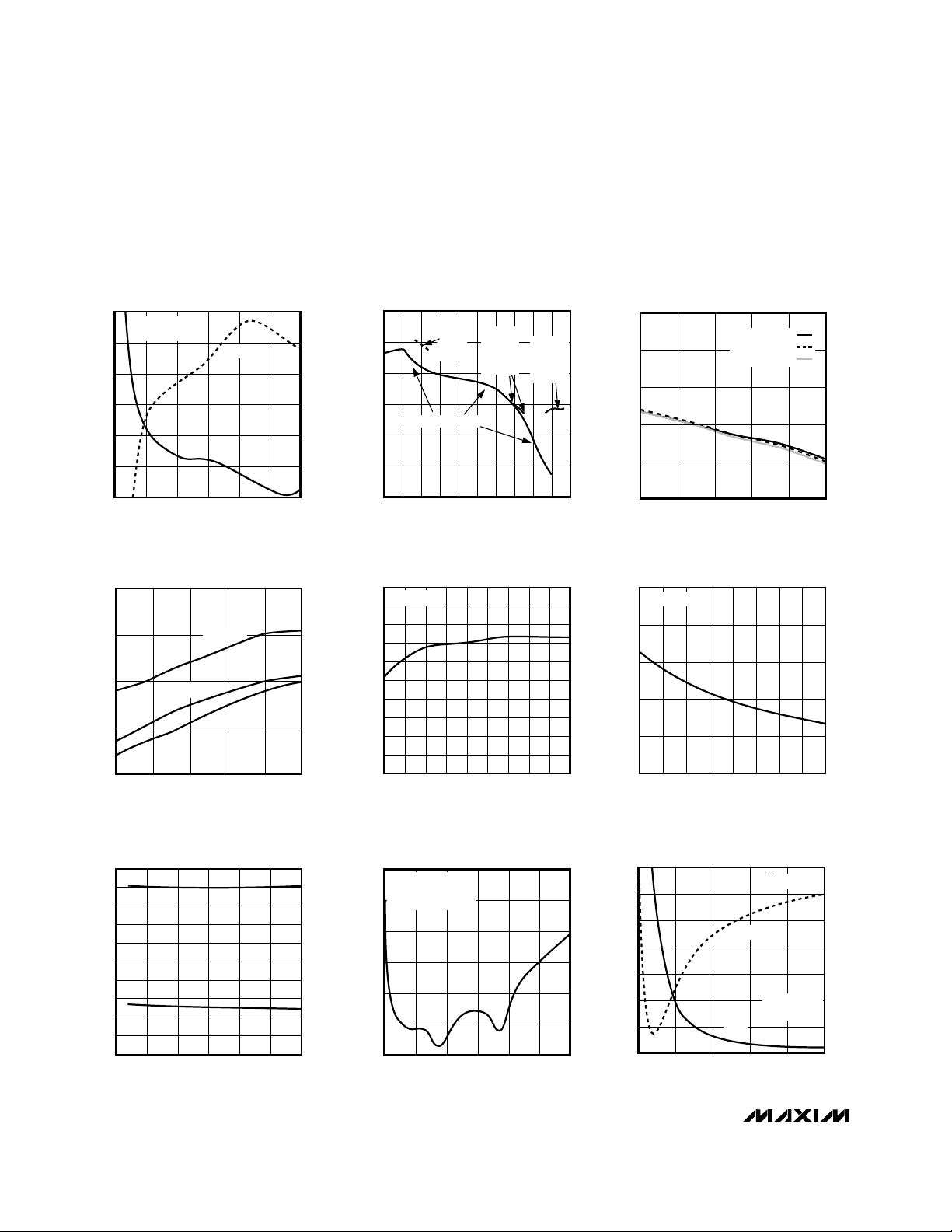
SUPPLY CURRENT vs. TEMPERATURE
MAX2406-01
TEMPERATURE (°C)
SUPPLY CURRENT (mA)
VCC = 5.5V
VCC = 3.0V
VCC = 2.7V
0
0.5
1.0
1.5
2.0
-40 -15 10 35 60 85
SHUTDOWN SUPPLY CURRENT
vs. TEMPERATURE
MAX2406-02
TEMPERATURE (°C)
SHUTDOWN SUPPLY CURRENT ( µA)
VCC = 5.5V
VCC = 4V
VCC = 3V
VCC = 2.7V
0
40
20
80
60
100
120
-200
-120
-160
-40
-80
0
40
0 1000 1500500 2000 2500 3000
LNA INPUT IMPEDANCE vs. FREQUENCY
MAX2406-03A
FREQUENCY (MHz)
REAL IMPEDANCE (Ω)
IMAGINARY IMPEDANCE (Ω)
IMAGINARY
MEASURED AT
DEVICE PIN
REAL
REAL
0
100
50
200
150
250
300
-120
-80
-100
-40
-60
-20
0
0 1000 1500500 2000 2500 3000
LNA OUTPUT IMPEDANCE
vs. FREQUENCY
MAX2406-03B
FREQUENCY (MHz)
REAL IMPEDANCE (Ω)
IMAGINARY IMPEDANCE (Ω)
MEASURED AT
DEVICE PIN
IMAGINARY
-12
-11
-9
-10
-8
-7
-40 10-15 35 60 85
LNA INPUT IP3 vs. TEMPERATURE
MAX2406-06
TEMPERATURE (°C)
INPUT IP3 (dBm)
VCC = 5.5V
VCC = 3.0V
VCC = 2.7V
0
5
10
15
20
25
800 16801240 2120 2560 3000
LNA GAIN vs. FREQUENCY
MAX2406-04
FREQUENCY (MHz)
GAIN (dB)
WITH 1pF SHUNT
CAPACITOR AT INPUT
WITHOUT 1pF SHUNT
CAPACITOR AT INPUT
12
14
18
16
20
22
-40 10-15 35 60 85
LNA GAIN vs. TEMPERATURE
MAX2406-05
TEMPERATURE (°C)
GAIN (dB)
VCC = 5.5V
VCC = 4V
VCC = 3V
VCC = 2.7V
-10
-8
-4
-6
-2
0
-40 10-15 35 60 85
LNA OUTPUT 1dB COMPRESSION POINT
vs. TEMPERATURE
MAX2406-07
TEMPERATURE (°C)
OUTPUT 1dB COMPRESSION POINT (dBm)
VCC = 5.5V
VCC = 3.0V
VCC = 2.7V
0.0
1.0
0.5
2.0
1.5
3.0
2.5
3.5
4.5
4.0
5.0
100 480 860 1240 1620 2000
LNA NOISE FIGURE vs. FREQUENCY
MAX2406-09
FREQUENCY (MHz)
NOISE FIGURE (dB)
__________________________________________Typical Operating Characteristics
(MAX2406EVKIT, Rev. B, VCC= 3.3V, RXEN = VCC, ƒLO= 1.5GHz, ƒ
LNAIN
= ƒ
RXMXIN
= 1.9GHz, P
LNAIN
= -30dBm,
P
RXMXIN
= -21.5dBm, PLO= -10dBm, differential IF operation, 50Ω system, TA= +25°C, unless otherwise noted.)
Page 4
MAX2406
Low-Cost Downconverter
with Low-Noise Amplifier
4 _______________________________________________________________________________________
____________________________Typical Operating Characteristics (continued)
(MAX2406EVKIT, Rev. B, VCC= 3.3V, RXEN = VCC, ƒLO= 1.5GHz, ƒ
LNAIN
= ƒ
RXMXIN
= 1.9GHz, P
LNAIN
= -30dBm,
P
RXMXIN
= -21.5dBm, PLO= -10dBm, differential IF operation, 50Ω system, TA= +25°C, unless otherwise noted.)
0
100
50
200
150
250
300
-350
-250
-300
-150
-200
-100
-50
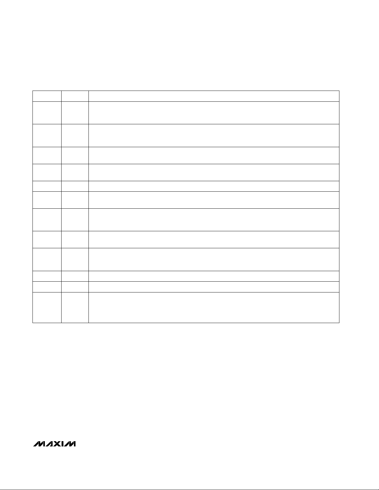
0 1000 1500500 2000 2500 3000
RX MIXER INPUT IMPEDANCE
vs. FREQUENCY
MAX2406-10
FREQUENCY (MHz)
REAL IMPEDANCE (Ω)
IMAGINARY IMPEDANCE (Ω)
REAL
MEASURED AT
DEVICE PIN
IMAGINARY
-10
-5
0
5
10
15
20
0.3 0.6 0.9 1.2 1.5 1.8 2.1 2.4 2.7 3.0 3.3
MIXER GAIN vs. FREQUENCY
MAX2406-11
FREQUENCY (GHz)
GAIN (dB)
900MHz
NARROW-
BAND
MATCH
2.4GHz
NARROW-
BAND
MATCH
3GHz
NARROW-
BAND
MATCH
1.9GHz EV KIT MATCH
5
7
11
9
13
15
-40 10-15 35 60 85
MIXER GAIN vs. TEMPERATURE
MAX2406-12
TEMPERATURE (°C)
GAIN (dB)
VCC = 5.5V
V
CC
= 4.0V
V
CC
= 2.7V, 3.0V
3
4
5
6
7
-40 10-15 35 60 85
MIXER INPUT IP3 vs. TEMPERATURE
MAX2406-13
TEMPERATURE (°C)
INPUT IP3 (dBm)
VCC = 5.5V
VCC = 3.0V
VCC = 2.7V
0
3
2
1
4
5
6
7
8
9
10
2.5 3.53.0 4.0 4.5 5.0 5.5
LNA AND MIXER NOISE FIGURE
vs. SUPPLY VOLTAGE
MAX2406-16
SUPPLY VOLTAGE (V)
NOISE FIGURE (dB)
MIXER
LNA
5.0
6.0
5.5
7.0
6.5
8.0
7.5
8.5
9.5
9.0
10.0
-18 -14 -12 -10-16 -8 -6 -4 -2 0
MIXER GAIN vs. LO POWER
MAX2406-14
LO POWER (dBm)
GAIN (dB)
VCC = 3.0V
5
7
11
9
13
15
-18 -14 -12-16 -10 -8 -6 -4 0
MIXER NOISE FIGURE vs. LO POWER
MAX2406-15
LO POWER (dBm)
NOISE FIGURE (dB)
VCC = 3.0V
30
20
25
10
15
5
0
0 1000 1500500 2000 2500 3000
LO PORT RETURN LOSS
vs. FREQUENCY
MAX2406-17
FREQUENCY (MHz)
RETURN LOSS (dB)
MEASURED ON EV KIT
WITH 220pF SERIES C
AT LO PORT
0
200
100
400
300
600
500
700
-700
-500
-600
-300
-400
-100
-200
0
0 400200 600 800 1000
IF OUTPUT IMPEDANCE (SINGLE ENDED)
vs. FREQUENCY
MAX2406-18
FREQUENCY (MHz)
REAL IMPEDANCE (Ω)
IMAGINARY IMPEDANCE (Ω)
IF TIED TO V
CC
IMAGINARY
MEASURED AT
DEVICE PIN
REAL
Page 5
_______________Detailed Description
The following sections describe each of the blocks in
the MAX2406 Functional Diagram.
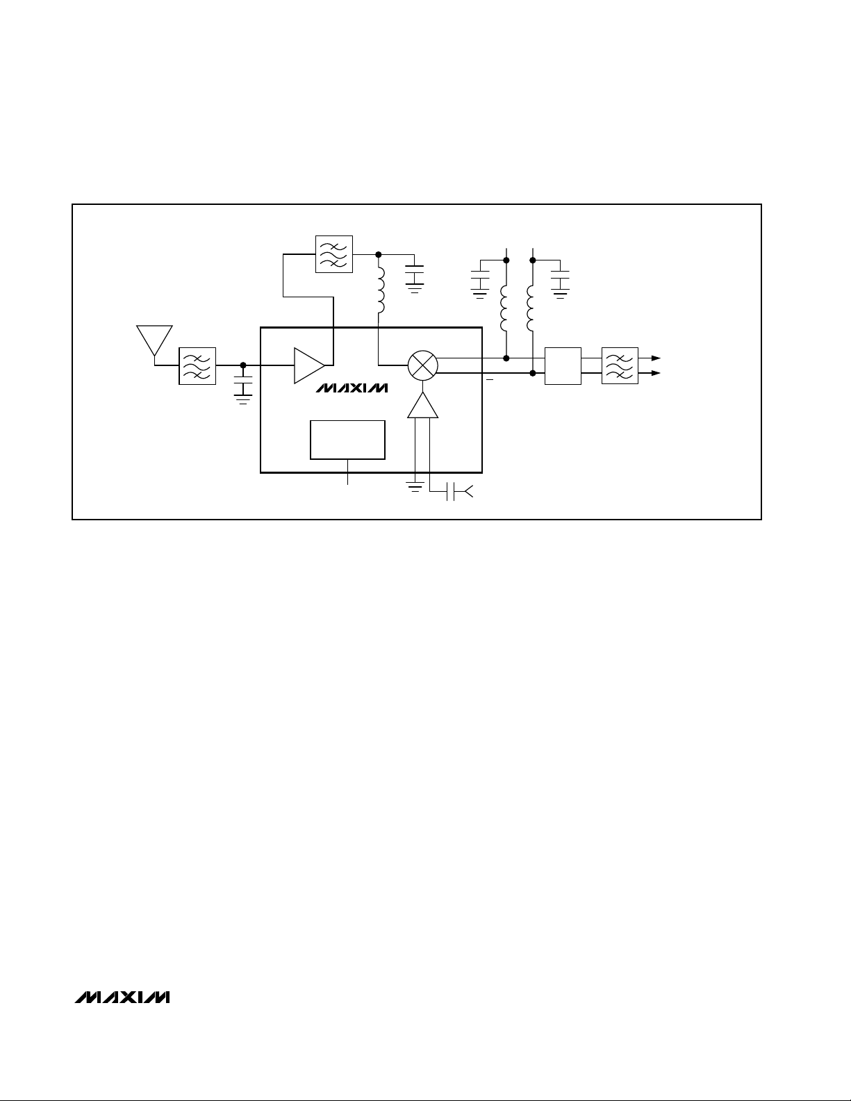
The MAX2406 consists of four major components: a lownoise amplifier (LNA), a downconverter mixer, a localoscillator (LO) buffer, and a power-management block.
Low-Noise Amplifier
The LNA is a wideband, single-ended cascode amplifier that can be used over a wide range of frequencies.
Refer to the LNA Gain vs. Frequency graph in the
Typical Operating Characteristics
. Its port impedances
are optimized for operation around 1.9GHz, requiring
only a 1pF shunt capacitor at the LNA input for a VSWR
of better than 2:1 at the input and output. As with every
LNA, the input match can be traded off for better noise
figure.
Receive Mixer
The receive mixer is a wideband, double-balanced
design with excellent noise figure and linearity.
RF Inputs
The RXMXIN input is typically connected to the LNA
output through an off-chip filter providing enhanced
flexibility. This input is externally matched to 50Ω. See
Figure 1 for an example matching network for 1.9GHz,
and the Rx Mixer Input Impedance vs. Frequency
graph in the
Typical Operating Characteristics
.
MAX2406
Low-Cost Downconverter
with Low-Noise Amplifier
_______________________________________________________________________________________ 5
______________________________________________________________Pin Description
NAME FUNCTION
1, 3, 4, 10,
11, 12,
15, 20
GND Ground. Connect to ground plane with minimal inductance.
2 LNAIN
RF Input to the LNA. At 1.9GHz, LNAIN can be easily matched to 50Ω with one external shunt 1pF
capacitor. AC couple to this pin. See the LNA Input Impedance vs. Frequency plot in the
Typical
Operating Characteristics
.
PIN
5, 9 V
CC
Supply Voltage (+2.7V to +5.5V). Bypass VCCto GND at each pin with a 47pF capacitor as close to each
pin as possible.
6 RXEN
Enable Control Input, active high. Logic high activates all part functions. A logic low places the device in
shutdown mode.
14
IF
Inverting Side of Downconverter’s Differential Open-Collector IF Output. Follow recommendations for IF
output above. If single-ended operation is desired, connect IF directly to V
CC
.
13 IF
Noninverting Side of Downconverter’s Differential Open-Collector IF Output. Pull IF up to VCCwith an
inductor. This inductor can be part of the matching network to the desired IF impedance. Alternatively, a
resistor can be placed in parallel to set a terminating impedance.
8
LO
50Ω Inverting Local-Oscillator Input Port. For single-ended LO operation, connect LO directly to GND. If
a differential LO signal is available, AC couple the inverted LO signal to this pin.
7 LO 50Ω Local-Oscillator Input Port. AC couple to this pin.
19 LNAOUT
LNA Output. This output typically provides a VSWR of better than 2:1 at frequencies from 1.8GHz to 2.5GHz
with no external matching components. At other frequencies, a matching network may be required to match
this pin to an external filter. Consult the LNA Output Impedance vs. Frequency plot in the
Typical Operating
Characteristics
.
16 RXMXIN
RF Input of Downconverter Mixer. AC couple to this pin. A matching network may be required to match
RXMXIN to an external filter. Consult the Rx Mixer Input Impedance vs. Frequency plot in the
Typical
Operating Characteristics.
17 GND LNA Output Ground. Connect to ground plane with minimal inductance.
18 GND Downconverter Mixer Input Ground. Connect to ground plane with minimal inductance.
Page 6
MAX2406
LO Inputs
The LO and LO pins are internally terminated with 50Ω
resistors. See the
Typical Operating Characteristics
for
a plot of LO Port Return Loss vs. Frequency. AC couple
the local-oscillator signal to these pins. If a singleended LO source is used, connect LO to ground.
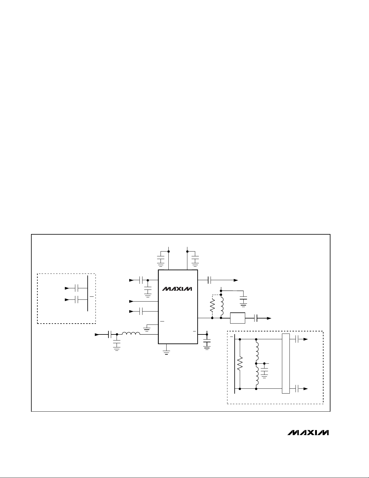
IF Output Port
The receive mixer output appears on the differential IF
and IF pins. These open-collector outputs each require
an external inductor to VCCfor DC biasing. This port
typically requires a matching network for coupling to an
external IF filter. For single-ended operation, connect
the unused side (typically IF) to VCC, and decouple it to
ground with a 1000pF capacitor. Figure 1 shows examples of single-ended and differential IF port connections. Refer to the IF and IF Output Impedance vs.
Frequency plot in the
Typical Operating Characteris-
tics
. At lower IF frequencies, a shunt resistor across the
pull-up inductor (in single-ended applications) or
across IF and IF (in differential applications) can be
used to set the IF impedance.
Power-Down Control
Pulling RXEN low places the MAX2406 in shutdown
mode. Power-down is guaranteed with a control voltage
at or below 0.6V. The device exits shutdown in 0.5µs
typical.
__________Applications Information
Extended Frequency Range
The MAX2406 has been characterized at 1.9GHz for
use in PCS applications; however, it operates over a
much wider frequency range. The LNA gain and noise
figure, as well as receive mixer conversion gain, are
plotted over a wide frequency range in the
Typical
Operating Characteristics
. When operating the device
at frequencies other than those specified in the specification table, it may be necessary to design or alter the
matching networks on LNAIN, RXMIXIN, IF, and (if
used) IF. In some cases, the internal broadband output
match on LNAOUT may have to be supplemented by
an external matching circuit. The
Typical Operating
Characteristics
provide port-impedance data vs. fre-
quency for use in designing a matching network. The
Low-Cost Downconverter
with Low-Noise Amplifier
6 _______________________________________________________________________________________
Figure 1. MAX2406 Typical Operating Circuit
MAX2406
V
CC
V
CC
V
CC
V
CC
V
CC
V
CC
RXMXIN IF
IF
LNAOUT LNA OUTPUT
*OPTIONAL
IF OUTPUT
(SINGLE-ENDED)
IF OUTPUT
DIFFERENTIAL
DIFFERENTIAL IF OPERATION
GND
LO
LO
RXEN
LNAINLNA INPUT
RECEIVER
ENABLE
LO INPUT
(SINGLE-ENDED)
RECEIVE
MIXER
INPUT
47pF47pF
2
95
19
13
L
CHOKE
L
CHOKE
L
CHOKE
14
14
13
1, 3, 4, 10,
11, 12, 15,
17, 18, 20
6
7
R*
R*
8
16
220pF 220pF
MATCH220pF
LO
DIFFERENTIAL LO OPERATION
LO INPUT
DIFFERENTIAL
7
8
220pF
220pF
1000pF
V
CC
1000pF
1000pF
1000pF
1000pF
1000pF
4.7nH
*1pF
220pF
1pF
IF
IF
LO
MATCH
Page 7
LO port is internally terminated to 50Ω and provides a
good match (a VSWR of approximately 1.2:1 to 2GHz,
and a VSWR of approximately 2:1 to 3GHz).
Layout
A properly designed PC board is an essential part of
any RF/microwave circuit. Be sure to use controlled
impedance lines on all high-frequency inputs and outputs, use low-inductance connections to ground on all
GND pins, and place decoupling capacitors close to all
VCCconnections.
For the power supplies, a star topology works well.
Each V
CC
node in the circuit has its own path to a central VCCand a decoupling capacitor that provides low
impedance at the RF frequency of interest. The central
VCCnode has a large decoupling capacitor as well.
This provides good isolation between the different sections of the MAX2406. The MAX2406 EV kit layout can
be used as a guide to integrating the MAX2406 into
your design.
MAX2406
Low-Cost Downconverter
with Low-Noise Amplifier
_______________________________________________________________________________________ 7
BIAS
CONTROL
MATCH
RX MIXER
IF
IF OUT
IF BPF
RF BPF
RF BPF
IF
LO SOURCE
LO
BUFFER
LNAIN
LNAOUT
RXEN
V
CCVCC
MAX2406
LNA
____________________________________Typical Application Functional Diagram
Page 8

MAX2406
Low-Cost Downconverter
with Low-Noise Amplifier
8 _______________________________________________________________________________________
________________________________________________________Package Information
QSOP.EPS
 Loading...