

Page 1
General Description
The MAX2387/MAX2388/MAX2389 low-noise amplifier
(LNA), downconverter mixers designed for W-CDMA
applications, are ideal for ARIB (Japan) and ETSIUMTS (Europe) based systems. The MAX2387/
MAX2388/MAX2389 feature ultra-low current consumption and exceptionally low noise figures in ultra-small
packages.
The MAX2387/MAX2388 include an LNA, a downconverter mixer, and a local-oscillator (LO) buffer. The
MAX2389 has an LNA and mixer, but minimizes current
consumption by omitting the LO buffer. For all devices,
the LNA and downconverter mixers are optimized for
the 2110MHz to 2170MHz band. All devices feature a
high-gain mode and a low-gain mode of LNA operation.
The MAX2387 has a 32dB gain step, and the
MAX2388/MAX2389 have an 18dB gain step. All ICs
include a shutdown mode, powering down the IC during the front-end receiver’s idle periods.
The mixer 3rd-order nonlinearity performance is set
using an external biasing resistor. For the MAX2387/
MAX2388, mixer performance is optimized for a
-10dBm typical drive at the LO buffer input port. The
MAX2389 mixer performance is optimized for a
-4dBm typical drive at the LO input port. The LO port
for all versions is configurable for either single-ended or
differential operation.
These devices operate from a +2.7V to +3.3V single supply and are available in ultra-small (3mm ✕3mm) 12-pin
leadless packages (QFN).
________________________Applications
Japanese 3rd-Generation W-CDMA Cellular
Phones
Dual-Mode W-CDMA/GSM Cellular Phones
Features
♦ Ultra-Low Current Consumption: 10.7mA
(MAX2387), 9.9mA (MAX2388), and 7.9mA
(MAX2389)
♦ +2.7V to +3.3V Single-Supply Operation
♦ Mixer NF: 7dB SSB
♦ Cascaded Noise Figure: 2.3dB
♦ LNA Low-Gain Mode: 32dB Gain Step (MAX2387)
or 18dB Gain Step (MAX2388/MAX2389)
♦ Mixer IIP3: 6dBm
♦ < 1µA Shutdown Current
♦ Ultra-Small (3mm
✕
3mm) 12-Pin QFN Package
MAX2387/MAX2388/MAX2389
W-CDMA LNA/Mixer ICs
________________________________________________________________ Maxim Integrated Products 1
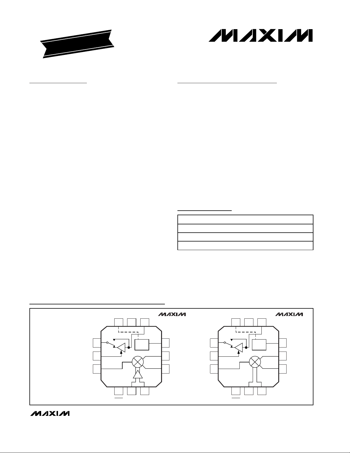
Pin Descriptions/Functional Diagrams
19-1834; Rev 1; 5/01
EVALUATION KIT
AVAILABLE
Ordering Information
For pricing, delivery, and ordering information, please contact Maxim/Dallas Direct! at
1-888-629-4642, or visit Maxim’s website at www.maxim-ic.com.
PART TEMP. RANGE PIN-PACKAGE
MAX2387EGC -40°C to +85°C 12 QFN
MAX2388EGC -40°C to +85°C 12 QFN
MAX2389EGC -40°C to +85°C 12 QFN
TOP VIEW
1LNA_OUT
2GAIN
3MIX_IN
BIAS11GND10LNA_IN
12
BIAS
45
LO+6LO-
SHDN
MAX2387/MAX2388
9 V
8 IF+
7 IF-
CC
1LNA_OUT
2GAIN
3MIX_IN
BIAS11GND10LNA_IN
12
BIAS
45
LO+6LO-
SHDN
MAX2389
9 V
8 IF+
7 IF-
CC
Page 2
MAX2387/MAX2388/MAX2389
W-CDMA LNA/Mixer ICs
2 _______________________________________________________________________________________
ABSOLUTE MAXIMUM RATINGS
DC ELECTRICAL CHARACTERISTICS
(VCC= +2.7V to +3.3V, SHDN = high, R
BIAS
= 24kΩ, no input AC signals, TA= -40°C to +85°C. Typical values are at VCC= +2.7V,
T
A
= +25°C, unless otherwise noted.)
Stresses beyond those listed under “Absolute Maximum Ratings” may cause permanent damage to the device. These are stress ratings only, and functional
operation of the device at these or any other conditions beyond those indicated in the operational sections of the specifications is not implied. Exposure to
absolute maximum rating conditions for extended periods may affect device reliability.
VCCto GND...........................................................-0.3V to +4.3V
SHDN, GAIN to GND..................................-0.3V to (V
CC
+ 0.3V)
AC Signals ....................................................................+1V peak
Digital Input Current .........................................................±10mA
Continuous Power Dissipation (T
A
= +70°C)
12-Pin QFN (derate 11.9mW/°C above T
A
= +70°C)...952mW
Operating Temperature Range ...........................-40°C to +85°C
Junction Temperature......................................................+150°C
Storage Temperature Range .............................-65°C to +150°C
Soldering Temperature (10s) ...........................................+300°C
AC ELECTRICAL CHARACTERISTICS
(MAX238_ EV kit, VCC= 2.7V, SHDN = high, f
RF_IN
= f
LNA_IN
= 2140MHz, fLO= 2330MHz (fIF= 190MHz). Mixer, LNA, and LO input
ports are driven with 50Ω sources. R
BIAS
= 24kΩ ±1%, PLO= -10dBm (MAX2387/MAX2388), PLO= -4dBm (MAX2389), PRF=
-30dBm. Typical values are at V
CC
= +2.7V, TA= +25°C, unless otherwise noted.)
Operating Supply Current I
Shutdown Supply Current I
Digital Input Logic High V
Digital Input Logic Low V
Input Logic High Current I
Input Logic Low Current I
PARAMETER SYMBOL CONDITIONS MIN TYP MAX UNITS
High-gain mode
CC
Low-gain mode
SHDN = low 0.2 1.0 µA
CC
IH
IL
VIN = V
IH
IL
VIN = V
IH
IL
MAX2387 10.7 12.4
MAX2388 9.9 11.7
MAX2389 7.9 9.3
MAX2387 7.2 8.7
MAX2388 6.7 8.1
MAX2389 4.7 5.7
2.0 V
0.6 V
1µA
-20 µA
mA
LNA PERFORMANCE: LOW-GAIN MODE (GAIN = HIGH)
RF Frequency Range (Note 1) f
Gain G
PARAMETER SYMBOL CONDITIONS MIN TYP MAX UNITS
RF
LNA
TA = +25°C 13.5 15 16.5
TA = -40°C to +85°C (Note 2) 12.9 17.0
2110 2170 MHz
dB
Page 3
MAX2387/MAX2388/MAX2389
W-CDMA LNA/Mixer ICs
_______________________________________________________________________________________ 3
AC ELECTRICAL CHARACTERISTICS (continued)
(MAX238_ EV kit, VCC= 2.7V, SHDN = high, f
RF_IN
= f
LNA_IN
= 2140MHz, fLO= 2330MHz (fIF= 190MHz). Mixer, LNA, and LO input
ports are driven with 50Ω sources. R
BIAS
= 24kΩ ±1%, PLO= -10dBm (MAX2387/MAX2388), PLO= -4dBm (MAX2389), PRF=
-30dBm. Typical values are at V
CC
= +2.7V, TA= +25°C, unless otherwise noted.)
Noise Figure (Notes 1, 3) NF
3rd-Order Input Intercept Point
(Note 4)
Input -1dB Compression Point
(Note 1)
LNA PERFORMANCE: LOW-GAIN MODE (GAIN = LOW)
Gain G
Noise Figure (Notes 1, 3) NF
3rd-Order Input Intercept Point
(Note 5)
Input -1dB Compression Point IP
MIXER PERFORMANCE (GAIN = HIGH)
RF Frequency Range (Note 1) f
LO Frequency Range (Note 1) f
IF Frequency Range (Note 1) f
Power Conversion Gain G
PARAMETER SYMBOL CONDITIONS MIN TYP MAX UNITS
LNA
IIP3
LNA
IP
-1dB
LNA
LNA
IIP3
LNA
-1dB
RF
LO
IF
MXR
MXR
TA = +25°C 1.7 2.2 dB
TA = -40°C to +85°C (Note 2) 4.2 dBm
TA = +25°C
TA = -40°C to +85°C
(Note 2)
TA = +25°C 8.5 10 11.5
TA = -40°C to +85°C (Note 2) 7.5 12.5
TA = +25°C
-19 -13 dBm
MAX2387 -18.5 -16.5 -14.5
MAX2388/
MAX2389
MAX2387 -10.5 -14
MAX2388/
MAX2389
MAX2387 19.2 21.3
MAX2388/
MAX2389
MAX2387 1
MAX2388/
MAX2389
MAX2387 -9.9
MAX2388/
MAX2389
MAX2387 7.2 8.8
MAX2388 6.8 8.2Noise Figure (SSB) (Note 1) NF
MAX2389 7.3 9.5
-4.7 -2.8 -0.9
5.4 -0.7
6.5 8.4
3.4
-7.7
2110 2170 MHz
2250 2600 MHz
150 400 MHz
dB
dB
dBm
dBm
dB
dB
Page 4
MAX2387/MAX2388/MAX2389
W-CDMA LNA/Mixer ICs
4 _______________________________________________________________________________________
AC ELECTRICAL CHARACTERISTICS (continued)
(MAX238_ EV kit, VCC= 2.7V, SHDN = high, f
RF_IN
= f
LNA_IN
= 2140MHz, fLO= 2330MHz (fIF= 190MHz). Mixer, LNA, and LO input
ports are driven with 50Ω sources. R
BIAS
= 24kΩ ±1%, PLO= -10dBm (MAX2387/MAX2388), PLO= -4dBm (MAX2389), PRF=
-30dBm. Typical values are at V
CC
= +2.7V, TA= +25°C, unless otherwise noted.)
Note 1: Guaranteed by design and characterization.
Note 2: MIN guaranteed by production test, MAX guaranteed by design and characterization.
Note 3: Includes input matching circuit loss.
Note 4: f
IN1
= 2140MHz, f
IN2
= 2141MHz, PIN= -30dBm per tone.
Note 5: f
IN1
= 2140MHz, f
IN2
= 2141MHz, PIN= -25dBm per tone.
3rd-Order Input Intercept Point
(Notes 1, 3)
Input -1dB Compression Point
(Note 1)
MIXER PERFORMANCE (GAIN = LOW)
Power Conversion Gain (Note 1) G
3rd-Order Input Intercept Point
(Note 4)
Input -1dB Compression Point
(Note 1)
PARAMETER SYMBOL CONDITIONS MIN TYP MAX UNITS
IIP3
MXR
IP
- 1dB,M XRTA
MXR
MXR
IIP3
MXR
IP
- 1dB,M XRTA
= -40°C to +85°C
TA = +25°C 7.5 9.0 10.5
TA = -40°C to +85°C 6.5 12.0
TA = +25°C
TA = +25°C
= -40°C to +85°C
MAX2387 6
MAX2388 6
MAX2389 5
MAX2387 -13.9 -10
MAX2388 -16.3 -10.5
MAX2389 -15.4 -10.5
MAX2387 6.9 8.4
MAX2388 6.1 7.4Noise Figure (SSB) (Note 1) NF
MAX2389 6.6 8.8
MAX2387 0.7
MAX2388 0.2
MAX2389 1.3
MAX2387 -15.0 -10.7
MAX2388 -18.2 -11.3
MAX2389 -17.8 -11.9
dBm
dBm
dB
dB
dBm
dBm
Page 5

MAX2387/MAX2388/MAX2389
W-CDMA LNA/Mixer ICs
_______________________________________________________________________________________ 5
)
)
)
Typical Operating Characteristics
(TA = +25°C, VCC= +2.7V, unless otherwise noted.)
MAX2387
SUPPLY CURRENT vs. TEMPERATURE
MAX2387/88/89 toc01
GAIN (dB)
20
15
10
-5
-10
-15
-20
16
VCC = +2.7V
14
HIGH-GAIN
12
10
VCC = +2.7V
LOW-GAIN
8
SUPPLY CURRENT (mA)
6
4
2
-40 10-15 356085
VCC = +3.3V
LOW-GAIN
TEMPERATURE (°C)
VCC = +4.3V
HIGH-GAIN
VCC = +4.3V
LOW-GAIN
VCC = +3.3V
HIGH-GAIN
MAX2387
MIXER CONVERSION GAIN
vs. LO INPUT POWER
12
10
8
6
4
CONVERSION GAIN (dB)
2
0
-13 -11 -10-12 -9-8-7
LO INPUT LEVEL (dBm)
HIGH-GAIN MODELOW-GAIN MODE
MAX2387/88/89 toc04
30
25
20
15
10
IIP (dBm)
-5
-10
MAX2387
MIXER LO-IF AND LO-RF ISOLATION
vs. LO FREQUENCY
40
35
LO-RF: LOW-GAIN
MODE
30
25
LO-IF: LOW-GAIN
20
MODE
ISOLATION (dB)
15
10
LO-IF: HIGH-GAIN
5
MODE
0
2300 23202310 2330 2340 2350 2360
LO-RF: HIGH-GAIN
MODE
FREQUENCY (MHz
VCC = +2.7V
LO = -10dBm
MAX2387/88/89 toc07
NOISE FIGURE (dB)
25
20
15
10
LNA GAIN vs. TEMPERATURE
5
0
-40 -15 10 35 60 85
MIXER IIP2 AND IIP3 vs. TEMPERATURE
IIP2: HIGH-GAIN
MODE, SINGLEENDED LO
5
0
IIP3: HIGH-GAIN
MODE
-40 -15 10 35 60 85
LNA NOISE FIGURE vs. FREQUENCY
5
0
2110 21302120 2140 2150 2160 2170
MAX2387
HIGH-GAIN MODE
LOW-GAIN MODE
TEMPERATURE (°C)
MAX2387
IIP3: LOW-GAIN
MODE
TEMPERATURE (°C)
MAX2387
LOW-GAIN MODE
HIGH-GAIN MODE
FREQUENCY (MHz
IIP2: HIGH-GAIN
MODE, DIFFERENTIAL
LO
10
8
MAX2387/88/89 toc02
6
4
2
0
IIP3 (dBm)
-2
-4
-6
-8
-10
-40 10-15 35 60 85
MIXER INPUT -1dB COMPRESSION POINT
-6
-8
MAX2387/88/89 toc05
-10
-12
-14
-1dB COMPRESSION POINT (dBm)
-16
-40 10-15 35 60 85
MIXER NOISE FIGURE vs. LO POWER
8
MAX2387/88/89 toc08
7
6
NOISE FIGURE (dB)
5
4
-13 -10-12 -11 -9 -8 -7
MAX2387
LNA IIP3 vs. TEMPERATURE
HIGH-GAIN MODE
LOW-GAIN MODE
TEMPERATURE (°C)
MAX2387
vs. TEMPERATURE
TEMPERATURE (°
C
MAX2387
HIGH-GAIN MODE
LOW-GAIN MODE
LO POWER (dB)
MAX2387/88/89 toc03
MAX2387/88/89 toc06
MAX2387/88/89 toc09
Page 6

MAX2387/MAX2388/MAX2389
W-CDMA LNA/Mixer ICs
6 _______________________________________________________________________________________
Typical Operating Characteristics (continued)
(TA = +25°C, VCC= +2.7V, unless otherwise noted.)
SUPPLY CURRENT vs. TEMPERATURE
16
14
VCC = +2.7V
HIGH-GAIN
12
10
8
SUPPLY CURRENT (mA)
6
VCC = +2.7V
4
LOW-GAIN
2
-40 10-15 35 60 85
MAX2388
VCC = +3.3V
HIGH-GAIN
VCC = +4.3V
LOW-GAIN
VCC = +3.3V
LOW-GAIN
TEMPERATURE (°C)
VCC = +4.3V
HIGH-GAIN
MAX2387/88/89 toc10
GAIN (dB)
LNA GAIN vs. TEMPERATURE
20
15
10
5
0
-5
-40 10-15 35 60 85
HIGH-GAIN MODE
LOW-GAIN MODE
TEMPERATURE (°C)
MAX2388
MAX2387/88/89 toc11
IIP3 (dBm)
MAX2388
LNA IIP3 vs. TEMPERATURE
10
8
6
4
2
0
-2
-4
-6
-8
-10
-40 10-15 356085
HIGH-GAIN MODE
LOW-GAIN MODE
TEMPERATURE (°C)
MAX2387/88/89 toc12
MAX2388
MIXER CONVERSION GAIN
12
vs. LO INPUT POWER
10
8
6
4
CONVERSION GAIN (dB)
2
0
-13 -11 -10-12 -9-8-7
LO INPUT LEVEL (dBm)
HIGH-GAIN MODELOW-GAIN MODE
MAX2387/88/89 toc13
MIXER IIP2 AND IIP3 vs. TEMPERATURE
30
25
IIP2: HIGH-GAIN
20
MODE,
SINGLE-ENDED LO
15
10
IIP (dBm)
5
0
IIP3: HIGH-GAIN
-5
MODE
-10
-40 -15 10 35 60 85
MAX2388
IIP2: HIGH-GAIN
MODE, DIFFERENTIAL LO
IIP3: LOW-GAIN
MODE
TEMPERATURE (°C)
MAX2388
MIXER LO-IF AND LO-RF ISOLATION
vs. LO FREQUENCY
40
35
LO-RF: LOW-GAIN
MODE
30
25
LO-IF: LOW-GAIN
20
MODE
ISOLATION (dB)
15
10
LO-IF: HIGH-GAIN
5
MODE
0
2300 23202310 2330 2340 2350 2360
FREQUENCY (MHz)
LO-RF: HIGH-GAIN
MODE
VCC = +2.7V
LO = -10dBm
MAX2387/88/89 toc16
NOISE FIGURE (dB)
LNA NOISE FIGURE vs. FREQUENCY
10
8
6
4
2
0
2110 21302120 2140 2150 2160 2170
MAX2388
LOW-GAIN MODE
HIGH-GAIN MODE
FREQUENCY (MHz)
MIXER INPUT -1dB COMPRESSION POINT
-6
-8
MAX2387/88/89 toc14
-10
-12
-14
-1dB COMPRESSION POINT (dBm)
-16
-40 10-15 35 60 85
MIXER NOISE FIGURE vs. LO POWER
8
MAX2387/88/89 toc17
7
6
NOISE FIGURE (dB)
5
4
-13 -10-12 -11 -9 -8 -7
MAX2388
vs. TEMPERATURE
MAX2387/88/89 toc15
TEMPERATURE (°C)
MAX2388
HIGH-GAIN MODE
MAX2387/88/89 toc18
LOW-GAIN MODE
LO POWER (dB)
Page 7

MAX2387/MAX2388/MAX2389
W-CDMA LNA/Mixer ICs
_______________________________________________________________________________________ 7
Typical Operating Characteristics (continued)
(TA = +25°C, VCC= +2.7V, unless otherwise noted.)
SUPPLY CURRENT vs. TEMPERATURE
12
10
8
VCC = +2.7V
6
HIGH-GAIN
4
SUPPLY CURRENT (mA)
2
0
-40 10-15 356085
12
10
8
6
4
CONVERSION GAIN (dB)
2
0
-13 -11 -10-12 -9-8-7
MIXER LO-IF AND LO-RF ISOLATION
50
45
LO-RF: LOW-GAIN
40
MODE
35
LO-IF: LOW-GAIN
MODE
30
ISOLATION (dB)
25
20
LO-IF: HIGH-GAIN
MODE
15
10
2300 23202310 2330 2340 2350 2360
MAX2389
VCC = +3.3V
HIGH-GAIN
VCC = +2.7V
LOW-GAIN
TEMPERATURE (°C)
VCC = +4.3V
HIGH-GAIN
VCC = +4.3V
LOW-GAIN
VCC = +3.3V
LOW-GAIN
MAX2389
MIXER CONVERSION GAIN
vs. LO INPUT POWER
HIGH-GAIN MODELOW-GAIN MODE
LO INPUT LEVEL (dBm)
MAX2389
vs. LO FREQUENCY
LO-RF: HIGH-GAIN
MODE
VCC = +2.7V
LO = -4dBm
FREQUENCY (MHz)
MAX2387/88/89 toc19
GAIN (dB)
MAX2387/88/89 toc22
IIP (dBm)
MAX2387/88/89 toc25
NOISE FIGURE (dB)
20
15
10
-5
30
25
20
15
10
5
0
-5
-10
10
8
6
4
2
0
LNA GAIN vs. TEMPERATURE
MAX2389
HIGH-GAIN MODE
5
0
-40 10-15 35 60 85
LOW-GAIN MODE
TEMPERATURE (°C)
MAX2389
MIXER IIP2 AND IIP3 vs. TEMPERATURE
IIP2: HIGH-GAIN
MODE,
SINGLE-ENDED LO
IIP3: HIGH-GAIN
MODE
-40 -15 10 35 60 85
TEMPERATURE (°C)
IIP2: HIGH-GAIN
MODE,
DIFFERENTIAL LO
IIP3: LOW-GAIN
MODE
MAX2389
LNA NOISE FIGURE vs. FREQUENCY
LOW-GAIN MODE
HIGH-GAIN MODE
2110 21302120 2140 2150 2160 2170
FREQUENCY (MHz)
10
8
MAX2387/88/89 toc20
6
4
2
0
IIP3 (dBm)
-2
-4
-6
-8
-10
-40 10-15 356085
MIXER INPUT -1dB COMPRESSION POINT
-6
-8
MAX2387/88/89 toc23
-10
-12
-14
-1dB COMPRESSION POINT (dBm)
-16
-40 10-15 35 60 85
MIXER NOISE FIGURE vs. LO POWER
9
MAX2387/88/89 toc26
8
7
6
NOISE FIGURE (dB)
5
4
-7 -5-6 -4 -3 -2 -1
LNA IIP3 vs. TEMPERATURE
MAX2389
HIGH-GAIN MODE
LOW-GAIN MODE
TEMPERATURE (°C)
MAX2389
vs. TEMPERATURE
TEMPERATURE (°C)
MAX2389
HIGH-GAIN MODE
LOW-GAIN MODE
LO POWER (dB)
MAX2387/88/89 toc21
MAX2387/88/89 toc24
MAX2387/88/89 toc27
Page 8

MAX2387/MAX2388/MAX2389
Detailed Description
The MAX2387/MAX2388/MAX2389 include an LNA
and downconverter mixer. These devices feature a
shutdown mode to power down the IC during the frontend receiver’s idle periods. Each IC operates from a
+2.7V to +3.3V single supply and is housed in a 12-pin
ultra-small QFN (3mm ✕3mm) leadless package.
The MAX2387/MAX2388/MAX2389 are fabricated using
an advanced high-frequency silicon germanium
process. The LNA and mixer NF and IIP3 have been
optimized to provide excellent RF performance in the
2110MHz to 2170MHz band, while drawing minimal
current.
For the MAX2387/MAX2388, the mixer’s performance is
optimized for a -10dBm typical drive at the LO buffer
input port. The MAX2389’s mixer performance is optimized for a -4dBm typical drive at the LO input port.
The LO port for all versions can be driven either singleended or differentially.
LNA High/Low-Gain Mode
These devices offer two modes of operation for the LNA:
high-gain mode and low-gain mode, selectable with a
GAIN select pin. The MAX2387 has a gain of 15dB in
high-gain mode and -16.6dB in low-gain mode. The
MAX2388/MAX2389 have a gain of 15dB in high-gain
mode and -2.8dB in low-gain mode. Matching LNA in
high-gain mode will ensure matching in low-gain mode.
Downconverter Mixer
The receive mixer is a wideband, single-balanced
design with exceptional noise figure and linearity. The
LO input frequency range is 2330MHz to 2360MHz and
the RF input frequency range is 2110MHz to 2170MHz.
The mixer is internally matched to 50Ω, thus eliminating
any external matching components.
LO Input Buffers
The MAX2387/MAX2388 feature open-collector LO
buffers to increase isolation between the LO and the
rest of the system. The MAX2389 offers a lower current
consumption for applications that do not require an LO
buffer.
RF Inputs
The MIX_IN input is typically connected to the LNA output through an off-chip filter providing image rejection
and out-of-band interferers filtering. The LNA input and
output require an external matching network to 50Ω.
Note that the mixer input is internally matched to 50Ω.
See Figure 1, Typical Application Circuits for 2.14GHz.
LO Inputs
The LO+ and LO- pins are internally terminated with
100Ω resistors. AC-couple the local-oscillator signal to
these pins. If a single-ended LO source is used, connect LO+ to ground using an AC-coupling capacitor.
W-CDMA LNA/Mixer ICs
8 _______________________________________________________________________________________
Pin Description
PIN NAME FUNCTION
1 LNA_OUT RF Output Port for LNA. Requires external matching.
2 GAIN LNA/Mixer Gain Control Input
3 MIX_IN RF Input Port for Mixer. Internally matched to 50Ω.
4 SHDN
5 LO+
6 LO-
7 IF- Inverting Mixer’s IF Open-Collector Output
8 IF+ Noninverting Mixer’s IF Open-Collector Output
9VCCSupply Voltage (+2.7V to +3.3V). Capacitively bypass to GND near the IC.
10 LNA_IN RF Input Port for LNA. Requires external matching.
11 GND Ground
12 BIAS LNA/Mixer Bias Pin. For nominal bias, connect 24kΩ ±1% resistor to GND.
Shutdown Input. Drive low to enable shutdown mode. Drive high or connect to V
operation.
Noninverting LO Input for LO Buffer (MAX2387/MAX2388) or Mixer (MAX2389). Differential input
impedance is 200Ω. AC-couple to GND when the LO is driven single-endedly.
Inverting LO Input for LO Buffer (MAX2387/MAX2388) or Mixer (MAX2389). Differential input
impedance is 200Ω.
for normal
CC
Page 9

IF Output Port
The mixer output appears on the differential IF+ and IFpins. These open-collector outputs require an external
inductor to VCCfor DC biasing. This port typically
requires a matching network for coupling to an external
IF filter. Figures 1 and 2 show examples of differential
and single-ended IF port connections.
Applications Information
Layout
A properly designed PC board is essential to any
RF/microwave circuit. Keep RF signal lines as short as
possible to minimize losses and radiation. Always use
controlled impedance lines on all high-frequency inputs
and outputs and use low-inductance connections to
ground on all GND pins. At the mixer outputs, keep the
differential lines together and of the same length to
ensure signal balance.
For the best gain and noise performance, use highquality components for the LNA input matching circuit,
and solder the slug evenly to the board ground plane.
For the power supplies, a star topology works well to
isolate between different sections of the device. Each
V
CC
node has its own path to a central VCC. Place
decoupling capacitors that provide low impedance at
the RF frequency of interest close to all VCCconnections. The central VCCshould have a large decoupling
capacitor as well. (Use MAX2387/MAX2388/MAX2389
EV kit as an example.)
Chip Information
TRANSISTOR COUNT: 208
MAX2387/MAX2388/MAX2389
W-CDMA LNA/Mixer ICs
_______________________________________________________________________________________ 9
Figure 1. MAX2387/MAX2388/MAX2389 Differential IF Load; Single-Ended VCO
Typical Application Circuits
2.2nH
RX
24kΩ
GND
RX BPF
0.8pF
2.2nH
6800pF
0.8pF
TX
LNA_OUT
10nF
10kΩ
GAIN
20Ω
V
CC
MIX_IN
1
2
3
10nF
BIAS_SET
10kΩ
SHDN
12
11
MAX2387
MAX2388
MAX2389
45
82pF
LO+
BIAS
LNA_IN
10
6
LO-
82pF
VCO
V
CC V
6800pF
9
8
IF+
10kΩ
7
IF-
27nH
27nH
22pF
39pF
39pF
10µF
CC
IF
SAW
Z
L
Page 10

MAX2387/MAX2388/MAX2389
W-CDMA LNA/Mixer ICs
10 ______________________________________________________________________________________
Figure 2. MAX2387/MAX2388/MAX2389 Differential IF Load; Differential VCO
2.2nH
RX BPF
0.8pF
2.2nH
6800pF
10nF
BIAS
1
2
3
10kΩ
SHDN
24kΩ
MAX2387
MAX2388
MAX2389
RX
0.8pF
TX
LNA_OUT
10nF
10kΩ
GAIN
20Ω
V
CC
MIX_IN
GND
12
11
45
LO+
82pF
5.6nH
BIAS
9
IF+
8
IF-
7
V
CC
6800pF
27nH
10kΩ 27nH
IF
OUT
39pF
39pF
V
10nF
22pF
CC
IF
SAW
Z
L
LNA_IN
10
6
LO-
82pF
VCO
Page 11

MAX2387/MAX2388/MAX2389
W-CDMA LNA/Mixer ICs
Table 1. LNA Input/Output S-Parameters (VCC= +2.7V, High-Gain Mode)
Package Information
For the latest package outline information, go to
www.maxim-ic.com/packages.
Maxim cannot assume responsibility for use of any circuitry other than circuitry entirely embodied in a Maxim product. No circuit patent licenses are
implied. Maxim reserves the right to change the circuitry and specifications without notice at any time.
Maxim Integrated Products, 120 San Gabriel Drive, Sunnyvale, CA 94086 408-737-7600 ____________________ 11
© 2001 Maxim Integrated Products Printed USA is a registered trademark of Maxim Integrated Products.
S-PARAMETERS LNA (S11) LNA (S21) LNA (S12) LNA (S22)
FREQUENCY
(MHZ)
600 0.83287 -41.655 5.2176 146.82 0.020023 79.051 0.92461 -15.535
700 0.81889 -43.792 5.0791 145.33 0.021153 78.88 0.9171 -16.23
800 0.80364 -46.486 4.9464 143.26 0.022406 78.412 0.91098 -17.187
900 0.78522 -49.489 4.7767 141.09 0.023962 79.181 0.90108 -18.177
1000 0.76638 -53.118 4.6109 138.2 0.025913 78.989 0.8914 -19.536
1100 0.74542 -56.424 4.4363 135.68 0.027189 79.621 0.87913 -20.759
1200 0.72614 -59.477 4.2861 133.2 0.028484 79.666 0.86957 -22.045
1300 0.70338 -62.232 4.1209 130.93 0.030015 80.686 0.85623 -23.156
1400 0.68291 -64.933 4.0146 128.4 0.030979 81.41 0.84504 -24.46
1500 0.66114 -67.298 3.8951 126.82 0.032236 82.856 0.83313 -25.525
1600 0.63958 -69.782 3.7818 124.53 0.033056 83.763 0.82095 -26.882
1700 0.61641 -72.041 3.6761 122.88 0.03398 85.56 0.80875 -28.147
1800 0.59303 -74.571 3.5823 120.51 0.035009 86.377 0.79497 -29.825
1900 0.56989 -76.974 3.5198 118.87 0.036332 88.572 0.78338 -31.503
2000 0.54509 -79.651 3.4376 116.77 0.036887 89.686 0.76891 -33.44
2100 0.52084 -82.452 3.3691 115.17 0.038318 91.409 0.75735 -35.559
2200 0.49554 -85.891 3.2858 112.47 0.039355 93.409 0.74365 -38.175
2300 0.47232 -89.473 3.2544 110.28 0.040817 94.973 0.73415 -41.034
2400 0.44892 -93.529 3.195 108.05 0.042049 97.086 0.72262 -44.165
2500 0.42766 -98.164 3.1347 105.62 0.043438 98.58 0.71335 -47.828
2600 0.40833 -103.42 3.06 102.94 0.044844 100.14 0.70474 -51.733
2700 0.39421 -109.16 2.9818 100.13 0.046899 101.7 0.70067 -56.04
2800 0.38321 -115.32 2.9149 96.964 0.048389 103.31 0.69795 -60.397
2900 0.37608 -121.52 2.821 94.462 0.049426 104.62 0.69514 -64.899
3000 0.37573 -128.03 2.7086 91.479 0.05079 106.39 0.69504 -69.425
3100 0.38123 -134.23 2.5802 88.528 0.051657 108.22 0.69915 -73.798
3200 0.39208 -139.73 2.4696 85.584 0.053915 110.43 0.70504 -77.625
3300 0.40626 -144.57 2.3296 83.264 0.055483 113.29 0.71095 -81.166
3400 0.42512 -148.8 2.2157 80.95 0.05783 115.29 0.71819 -84.4
3500 0.44708 -152.13 2.0519 79.588 0.060614 118.09 0.72516 -87.06
3600 0.47302 -154.7 1.9382 77.337 0.065129 119.23 0.73416 -89.168
3700 0.49849 -156.57 1.8048 76.594 0.069104 120.99 0.73997 -90.676
MAGNITUDE PHASE MAGNITUDE PHASE MAGNITUDE PHASE MAGNITUDE PHASE
 Loading...