

Page 1
General Description
The MAX2374 silicon-germanium (SiGe), switchablegain, variable-linearity, low-noise amplifier (LNA) is
designed for cellular-band, code-division multipleaccess (CDMA). It can be used for applications such
as TDMA and PDC or wherever high dynamic range
and low noise are required. This LNA provides a high
intermodulation intercept point (IIP3), which is
adjustable to meet specific system requirements by
selecting an appropriate external resistor. To achieve
high gain and low noise, the LNA is packaged in a tiny
ultra-chip-scale package (UCSP) with six solder
bumps. The LNA operates from a +2.7V to +5.5V single
supply and consumes just 8.5mA while achieving a
+6.2dBm input IIP3. Supply current reduces to less
than 1µA in shutdown mode.
The MAX2374 provides two gain modes. High-gain
mode optimizes system sensitivity, while low-gain mode
optimizes system linearity.
Applications
CDMA Phones
TDMA Phones
Wireless Local Loop (WLL)
GSM Handsets
Land Mobile Radio
Wireless Data
Features
♦ +2.7V to +5.5V Single Supply
♦ Low Operating Current
8.5mA for High Linearity
4.5mA for Paging
4.1mA in Low-Gain, High-Linearity Mode
♦ Low Noise Figure: 1.5dB Cellular
♦ Adjustable IIP3
♦ Two Gain Settings
♦ < 1µA Shutdown Mode
♦ Ultra-Small 6-Bump UCSP (1mm x 1.5mm)
MAX2374
SiGe, Variable IIP3, Low-Noise Amplifier
in UCSP Package
________________________________________________________________ Maxim Integrated Products 1
19-1614; Rev 0; 6/00
EVALUATION KIT MANUAL
FOLLOWS DATA SHEET
Ordering Information
*UCSP reliability is integrally linked to the user’s assembly
methods, circuit board material, and environment. Refer to the
UCSP Reliability Notice in the UCSP Reliability section of this
data sheet for more information.
For free samples and the latest literature, visit www.maxim-ic.com or phone 1-800-998-8800.
For small orders, phone 1-800-835-8769.
Pin Configuration appears at end of data sheet.
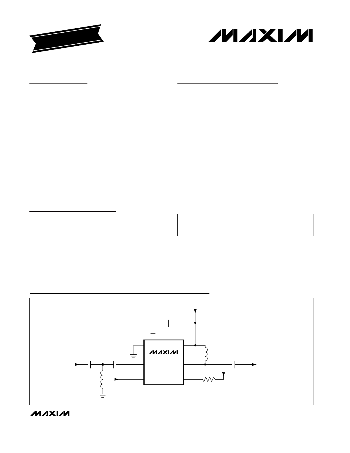
Typical Application Circuit
PART
MAX2374EBT
TEMP. RANGE
-40°C to +85°C
PINPACKAGE
6 UCSP*
TOP
MARK
AAB
+ 2.75V
V
CC =
100pF
A3
GND
5pF
LNA INPUT LNA OUTPUT
6.8nH
0.01µF
GAIN-CONTROL
LOGIC OUTPUT
MAX2374
A2
LNAIN
A1
GAIN
LNAOUT
V
BIAS
B3
CC
8.2nH
B2
B1
R
BIAS
2pF
V
CC
Page 2
MAX2374
SiGe, Variable IIP3, Low-Noise Amplifier
in UCSP Package
2 _______________________________________________________________________________________
ABSOLUTE MAXIMUM RATINGS
DC ELECTRICAL CHARACTERISTICS
(VCC= +2.7V to +5.5V, R
BIAS
= 20kΩ, V
GAIN
= high, LNAOUT = VCC, no input signals at LNAIN, TA= -40°C to +85°C. Typical values
are at V
CC
= +2.75V, TA= +25°C, unless otherwise noted.) (Note 1)
Stresses beyond those listed under “Absolute Maximum Ratings” may cause permanent damage to the device. These are stress ratings only, and functional
operation of the device at these or any other conditions beyond those indicated in the operational sections of the specifications is not implied. Exposure to
absolute maximum rating conditions for extended periods may affect device reliability.
VCCto GND...........................................................-0.3V to +6.0V
GAIN, BIAS Voltage to GND...................-0.3V to (V
CC
+ 0.3V)
GAIN, BIAS Current ......................................................±10mA
RF Input Power
LNAIN .........................................................................+10dBm
LNAOUT to GND ....................................-0.3V to (V
CC
+ 0.6V)
Continuous Power Dissipation (T
A
= +85°C) ...................540mW
Operating Temperature Range
MAX2374 .........................................................-40°C to +85°C
Storage Temperature.........................................-65°C to +150°C
Junction Temperature......................................................+150°C
VCC= 2.75V
GAIN = 0.6V, VCC= 2.75V
BIAS = open circuit
VCC= 5.5V
R
BIAS
= 10kΩ
R
BIAS
= 43kΩ
CONDITIONS
V
VCC-
1.16
BIAS Pin Voltage (Note 2)
µA-5 5Input Current
V0.6Input Logic Voltage Low
V1.5Input Logic Voltage High
µA0.1 1Shutdown Supply Current
8.5 10.5
V2.7 5.5Supply Voltage
mA
4.5 5.5
Supply Current
10.5
15
4.5
UNITSMIN TYP MAXPARAMETER
AC ELECTRICAL CHARACTERISTICS
(Typical Application Circuit, VCC= +2.7V to +5.5V, P
LNAIN
= -30dBm, V
GAIN
= high, f
LNAIN
= 881MHz, R
BIAS
= 20kΩ, TA= +25°C.
Typical values are at V
CC
= +2.75V, unless otherwise noted.) (Note 2)
VCC= 2.75V
All modes, f ≤ 6.5GHz
Input and output ports externally matched to 50Ω
V
GAIN
= high
CONDITIONS
10:1Maximum Stable Load VSWR
MHz750 1000
Recommended Operating Frequency
Range (Note 3)
dBm
-3.5
Output 1dB Compression
dB14Input and Output Return Loss
-20
6
UNITSMIN TYP MAXPARAMETER
V
GAIN
= high
V
GAIN
= low
V
GAIN
= low
dB
-9
Reverse Isolation
SUPPLY
GAIN CONTROL INPUT
Page 3
TA= -40°C to +85°C
MAX2374
SiGe, Variable IIP3, Low-Noise Amplifier
in UCSP Package
_______________________________________________________________________________________ 3
AC ELECTRICAL CHARACTERISTICS (continued)
(Typical Application Circuit, VCC= +2.7V to +5.5V, P
LNAIN
= -30dBm, V
GAIN
= high, f
LNAIN
= 881MHz, R
BIAS
= 18kΩ, TA= +25°C.
Typical values are at V
CC
= +2.75V, unless otherwise noted.) (Note 2)
VCC= 2.75V
CONDITIONS
dB1.5 1.7Noise Figure
dB
12.5 17
Gain
13.8 15 15.6
UNITSMIN TYP MAXPARAMETER
Note 1: Production tested at TA= +25°C. Maximum and minimum limits are guaranteed by design and characterization.
Note 2: Guaranteed by design and characterization.
Note 3: Operation over this frequency range is possible with a matching network tuned to the desired operating frequency.
Note 4: Measured with two-tone test with P
LNAIN
= -25dBm per tone, f1 = 881MHz, f2 = 881.9MHz.
0.4 1.2 2
Gain TA= -40°C to +85°C
-1 3.5
dB
Noise Figure 3 3.5 dB
TA= +25°C
TA= +25°C
TA= -40°C to +85°C
7.2
4.5 6.2
MAX2374 dBm
4.2
Input Third-Order Intercept Point (Note 4)
R
BIAS
= 10kΩ
R
BIAS
= 20kΩ
R
BIAS
= 43kΩ
10.5
5.8 7.2
Input Third-Order Intercept Point (Note 4) MAX2374
1
dBm
HIGH-GAIN MODE (GAIN = VCC)
LOW-GAIN MODE (GAIN = GND)
R
BIAS
= 10kΩ
R
BIAS
= 20kΩ
R
BIAS
= 43kΩ
12
10
8
6
4
2.5 4.03.0 3.5 4.5 5.0 5.5
ICC vs. V
CC
AND TEMPERATURE
MAX2374-01
VCC (V)
I
CC
(mA)
TA = -40°C
TA = +25°C
TA = +85°C
TA = +85°C
TA = +25°C
TA = -40°C
GAIN = V
CC
GAIN = GND
R
BIAS
= 20kΩ
-30
-20
0
-10
10
20
750 850800 900 950 1000
MAX2374-03
FREQUENCY (MHz)
MAGNITUDE (dB)
S21, S11, S22, S12 vs. FREQUENCY
S21
S11
S22
S12
V
CC
= GAIN = 2.75V
-20
-15
-5
-10
0
5
750 850800 900 950 1000
S21, S11, S22, S12 vs. FREQUENCY
MAX2374-04
FREQUENCY (MHz)
MAGNITUDE (dB)
S21
S12
S11
S22
V
CC
= 2.75V
GAIN = GND
TA= -40°C to +85°C
Typical Operating Characteristics
(Typical Application Circuit, VCC= +2.7V to +5.5V, P
LNAIN
= -30dBm, f
LNAIN
= 881MHz, R
BIAS
= 20kΩ, TA= +25°C, unless other-
wise noted.)
Page 4
MAX2374
SiGe, Variable IIP3, Low-Noise Amplifier
in UCSP Package
4 _______________________________________________________________________________________
Typical Operating Characteristics (continued)
(Typical Application Circuit, VCC= +2.7V to +5.5V, P
LNAIN
= -30dBm, f
LNAIN
= 881MHz, R
BIAS
= 20kΩ, TA= +25°C, unless other-
wise noted.)
LNA Output Port. This port requires an external pullup inductor, which may be used as part of the matching
network.
LNAOUTB2
Supply Voltage Input. Bypass with a 100pF capacitor to GND.V
CC
B3
LNA Bias Setting Pin. For nominal bias, connect 20kΩ resistor to VCC. Adjust the resistor value to alter the
linearity of the LNA.
BIASB1
Gain-Control Logic Input. Drive high for high-gain mode. Drive low for low-gain mode.GAINA1
PIN
LNA Input Port. Blocking capacitor is required, which may be used as part of the matching network.LNAINA2
Ground GNDA3
FUNCTIONNAME
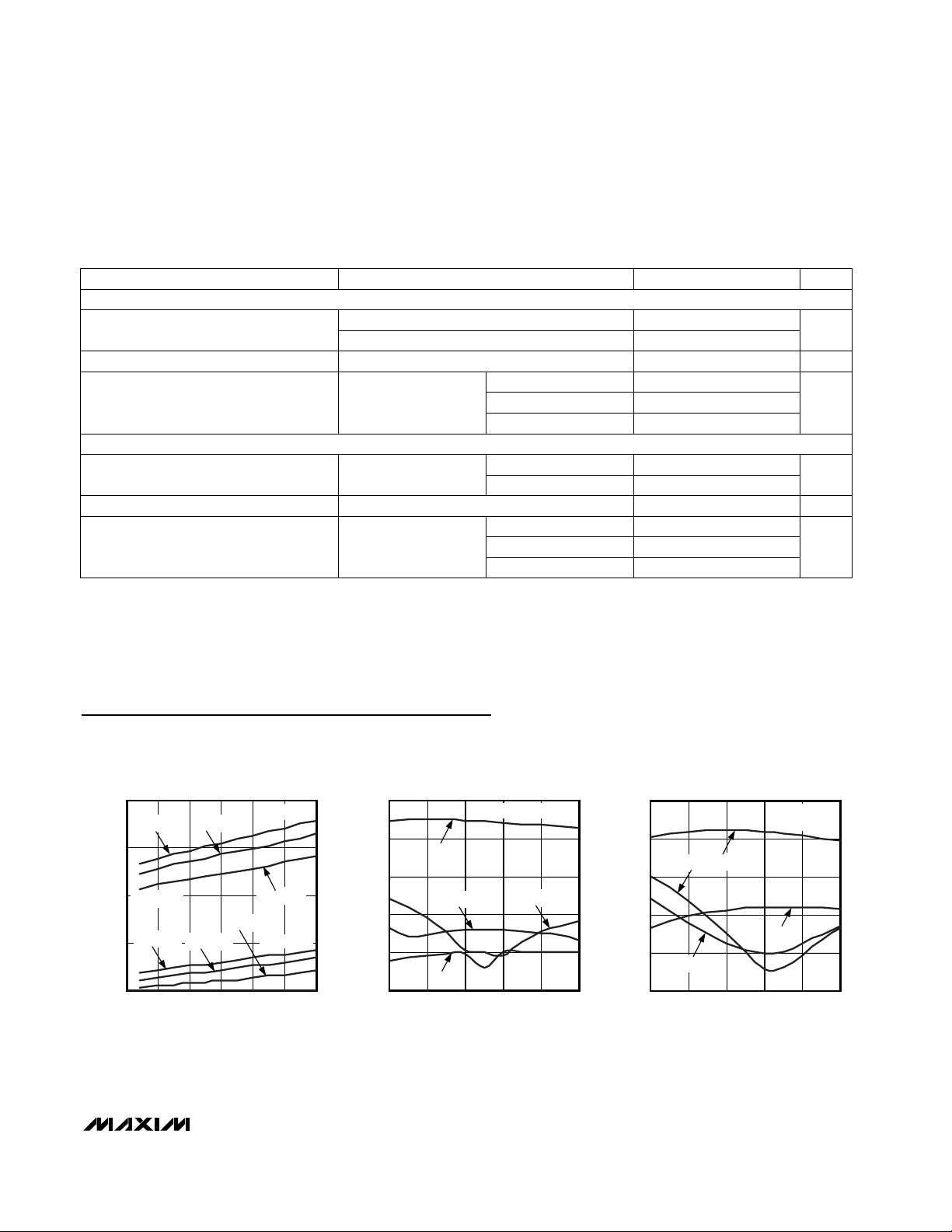
20
0
52515 35 45
GAIN vs. R
BIAS
AND TEMPERATURE
MAX2374-05
R
BIAS
(kΩ)
GAIN (dB)
15
10
5
TA = +85°C
TA = -40°C
TA = -40°C
TA = +25°C
TA = +85°C
TA = +25°C
GAIN = V
CC
GAIN = GND
V
CC
= 2.75V
0204060
IIP3 vs. R
BIAS
AND TEMPERATURE
MAX2374-06
R
BIAS
(kΩ)
IIP3 (dBm)
0
5
15
10
20
V
CC
= 2.75V,
f = 881MHz, 882MHz
= V
GAIN
= GND
A
= V
GAIN
= V
CC
B
TA = +25°C
TA = +85°C
TA = -40°C
TA = +85°C
A
B
B
TA = +25°C
TA = -40°C
Pin Description
4.5
4.0
3.5
3.0
2.5
NOISE FIGURE (dB)
2.0
1.5
1.0
750 850800 900 950 1000
NOISE FIGURE vs. FREQUENCY
V
= 2.75V
CC
GAIN = V
FREQUENCY (MHz)
CURRENT vs. VOLTAGE AND R
20
R
= 10kΩ, GAIN = V
MAX2374-07
(mA)
CC
I
CC
BIAS
15
R
= 20kΩ, GAIN = V
BIAS
10
5
0
2.5 4.03.0 3.5 4.5 5.0 5.5
R
BIAS
CC
R
= 43kΩ, GAIN = V
BIAS
R
= 20kΩ, GAIN = GND
BIAS
R
= 43kΩ, GAIN = GND
BIAS
VCC (V)
CC
= 10kΩ, GAIN = GND
BIAS
MAX2374-08
CC
Page 5
MAX2374
SiGe, Variable IIP3, Low-Noise Amplifier
in UCSP Package
_______________________________________________________________________________________ 5
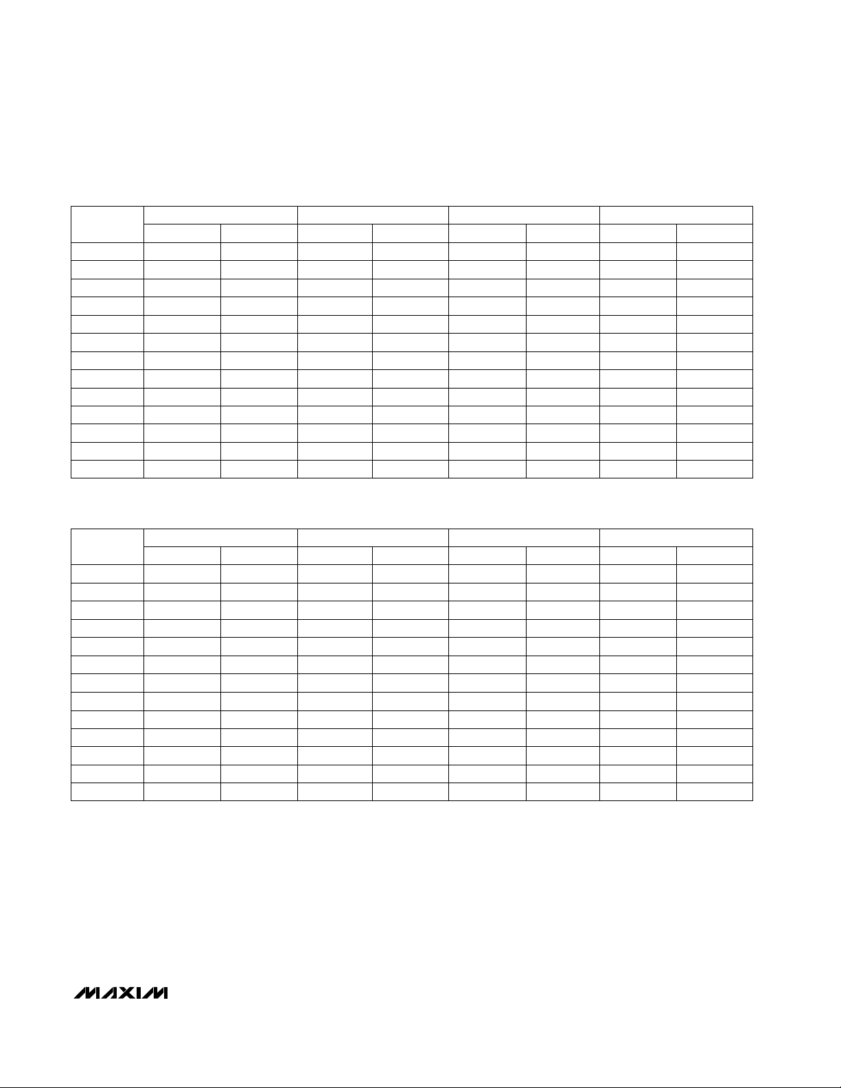
Table 1a. S-Parameters (VCC= V
GAIN
= 2.75V)
2250
2500
158.7
146.5
-20.2
78.8
-54.8
S22
0.626
3000
0.689
FREQ (MHz)
0.842
0.908
0.728
2750
250
128
MAGNITUDE
0.68
50
0.671
0.68
0.704
0.732
0.697
-12.9
-45.4
ANGLE
69
123.5
47.6
S12
0.693
500
ANGLE
33.3
21
11.19
5.042
15
17
1100.686
0.161
0.1
-81
0.026
0.007
-33.3
0.041
-370.078
MAGNITUDE
0.053
0.06
0.063
0.057
0.061
0.094
-60.5
750
-77
-105
122.73
-151.3
79.42
S21
0.074
ANGLE
49.35
24.18
1
-19.2
-35
-51
1.01
0.892
-128
9.83
12.84
6.19
-91.7
1000
0.781
MAGNITUDE
4.21
1250
3.12
2.38
1.771500
1.46
1.07
149
1750
139
-150
-49
2000
-11.89
-77.5
S11
125
ANGLE
-101
-123.7
-145.2
-165
176
163
0.664
0.691
-171
0.728
0.929
0.571
0.716
162
MAGNITUDE
0.524
0.529
0.568
0.612
0.639
0.652
-1040.662111.50.72
2250
2500
140
126.35
1.23
85.8
-42
S22
0.534
3000
0.623
FREQ (MHz)
0.471
0.374
0.596
2750
250
103.2
MAGNITUDE
0.659
50
0.689
0.694
0.695
0.681
0.629
-47
-77.2
ANGLE
85.7
127
52.2
S12
0.6
500
ANGLE
19.6
-9.33
-30.7
-47
-53.4
-42.5
85.80.566
0.175
0.123
-82
0.06
0.01
-62.8
0.14
-63.30.082
MAGNITUDE
0.189
0.2
0.184
0.146
0.117
0.096
-62
750
-89
-117.3
128.8
-148.7
72.4
S21
0.103
ANGLE
28.18
-6.87
-34.5
-54
-66
-66
0.196
0.156
-147.5
1.21
1.25
1
-83
1000
0.096
MAGNITUDE
0.772
1250
0.583
0.429
0.3011500
0.228
0.148
126.3
1750
112
-173
-42.4
2000
-8.93
-77
S11
92.4
ANGLE
-106
-132.7
-158
180
159.5
141.5
0.739
0.745
164.6
0.916
0.987
0.8
0.701
141.7
MAGNITUDE
0.75
0.754
0.782
0.803
0.811
0.797
-73.480.112730.591
Table 1b. S-Parameters (VCC= 2.75V, V
GAIN
= GND)
Page 6
MAX2374
SiGe, Variable IIP3, Low-Noise Amplifier
in UCSP Package
6 _______________________________________________________________________________________
Detailed Description
The MAX2374 SiGe LNA is packaged in a UCSP package in order to deliver high gain, high linearity, and low
noise in the smallest package possible. The special
feature of this LNA is that its linearity is adjusted by an
external resistor, R
BIAS
. The LNA has two digitally controllable gain modes to increase system dynamic
range. Digital high at GAIN selects the high-gain mode,
and digital low selects the low-gain mode.
Adjust the LNA bias current to control the amplifier’s linearity. The resistor R
BIAS
connected between BIAS and
VCCcontrols the LNA current. The amplifier’s linearity is
directly related to the operating current. Increasing the
bias current of the LNA increases the IIP3. V
BIAS
is
approximately constant at VCC- 1.16V. Connecting a
resistor from BIAS to VCCresults in a supply current
that can be calculated as follows:
VCC= (High Gain)
~
–
(150 - 1.16V) / R
BIAS
I
BIAS
can be set by a fixed resistor to VCCas described
above, or it can be generated with a switched network.
To operate the LNA in high-gain/high-linearity mode,
set R
BIAS
= 20kΩ and drive GAIN high. Do this in the
presence of a transmit signal to minimize cross-modulation. To operate the LNA in low-gain/low-linearity
mode, set R
BIAS
= 43kΩ and drive GAIN high. This
mode draws less current and should be used in the
absence of a transmit signal (paging mode). Shutdown
of the IC is accomplished by switching R
BIAS
to open
circuit.
Layout Issues
Design the layout for the IC to be as compact as possible to minimize the parasitics. The chip-scale IC package uses a bump pitch of 0.5mm (19.7mil) and bump
diameter of 0.3mm (~12mil). Therefore, lay out the solder-pad spacing on 0.5mm (19.7mil) centers, using a
pad size of 0.25mm (~10mil) and a solder mask opening of 0.33mm (13mil). Round or square pads are permissible. Connect multiple vias from the ground plane
as close to the ground pins as possible.
Install capacitors as close as possible to the IC supply
voltage pin and supply end of the series inductor.
Place the ground end of these capacitors near the IC
GND pins to provide a low-impedance return path for
the signal current.
Prototype Chip Installation
Alignment keys on the PC board around the area where
the chip is located will be helpful in the prototype
assembly process. It is better to align the chip on the
board before any other components are placed, and
then place the board on a hot plate or hot surface until
the solder starts melting. Remove the board from the
hot plate without disturbing the position of the chip, and
let it cool down to room temperature before processing
the board further.
UCSP Reliability
The ultra-chip-scale package (UCSP) represents a
unique packaging form factor that may not perform
equally well as a packaged product through traditional
mechanical reliability tests. UCSP reliability is integrally
linked to the user’s assembly methods, circuit board
material, and usage environment. The user should
closely review these areas when considering use of a
UCSP package.
Performance through operating-life test and moisture
resistance remains uncompromised as it is primarily
determined by the wafer-fabrication process.
Mechanical stress performance is a greater consideration for UCSP packages. UCSPs are attached through
direct solder contact to the user’s PC board, foregoing
the inherent stress relief of a packaged product lead
frame. Solder joint contact integrity must be considered. Comprehensive reliability tests have been performed and are available upon request. In conclusion,
the UCSP performs reliably through environmental
stresses.
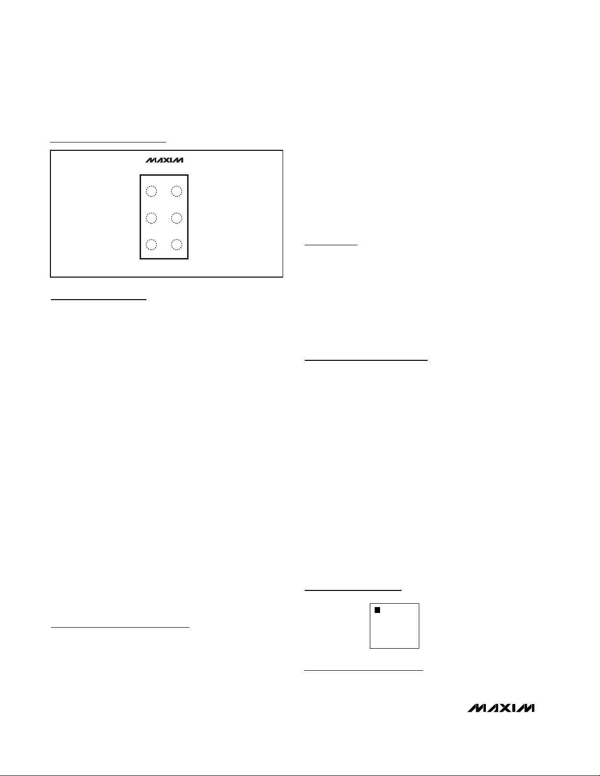
Marking Information
Pin Configuration
TRANSISTOR COUNT: 296
Chip Information
TOP VIEW
(BUMPS ON BOTTOM)
LNAIN
GAIN
MAX2374
A3GND
A2
A1
UCSP
V
B3
CC
LNAOUT
B2
B1
BIAS
ORIENTATION
A A A
A A A
PRODUCT ID CODE
LOT CODE
Page 7
MAX2374
SiGe, Variable IIP3, Low-Noise Amplifier
in UCSP Package
_______________________________________________________________________________________ 7
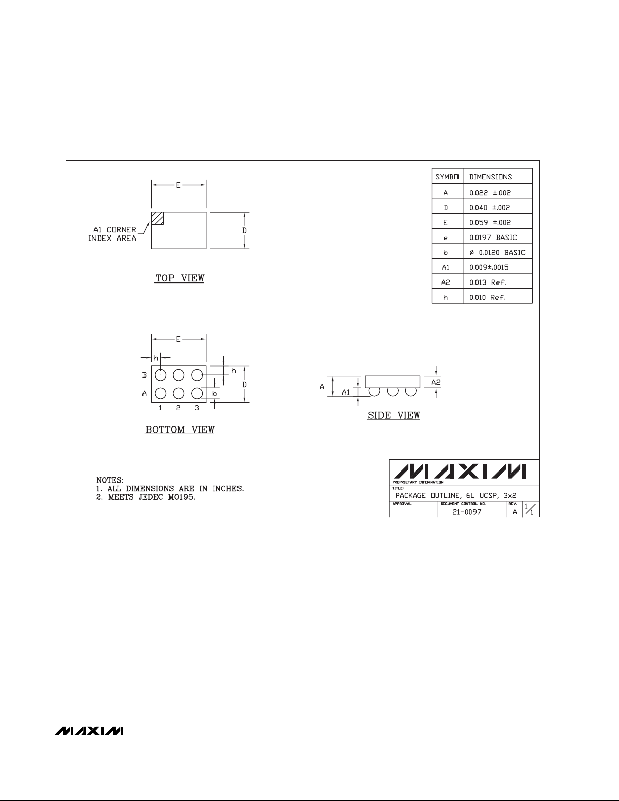
Package Information
6L,UCSP.EPS
Page 8

MAX2374
SiGe, Variable IIP3, Low-Noise Amplifier
in UCSP Package
8 _______________________________________________________________________________________
NOTES
 Loading...