

Page 1
________________General Description
The MAX2323/MAX2325 are low-noise amplifier (LNA)
plus mixer ICs optimized for code-division multiple-access
(CDMA) applications in both cellular and PCS bands. The
MAX2323 addresses dual-band, triple-mode CDMA applications by providing switched signal paths for cellular FM,
cellular CDMA, and PCS CDMA. The MAX2325 is a cellular-band dual-mode version.
To optimize cellular-band dynamic range at minimum current, the MAX2323/MAX2325 implement four LNA states:
high gain/high linearity, high gain/low linearity, midgain,
and low gain. In high-gain/high-linearity mode, the
adjustable high-intercept LNA minimizes desensitization in
the presence of a large interfering signal. For the other
gain states, the LNA current is reduced to improve standby time.
The CDMA mixers are designed for high linearity, low
noise, and differential IF outputs, while the FM mixer is
designed for lower current and single-ended output. Each
band is implemented with a separate mixer to optimize
performance for the specific band.
The MAX2323/MAX2325 can also be used in TDMA,
EDGE, and W-CDMA phones.
________________________Applications
Dual-Band, Triple-Mode PCS/Cellular Phones
Dual-Mode Cellular Phones
____________________________Features
♦ 2.7V Operation
♦ Dual Band, Triple Mode
♦ Three LNA Gain Settings (Cellular)
♦ Two LNA Gain Settings (PCS)
♦ 18mA in Low-Gain Mode
19.5mA in Paging and Midgain Mode
26.5mA in High-Gain, High-Linearity Mode
16.5mA in FM Mode, High-Gain, Low-Linearity
Mode
♦ 2.5dB (typ) Cascade Noise Figure
♦ Adjustable LNA IIP3, +5dBm to +13dBm
♦ Ultra-Small 28-Pin Package (5mm x 5mm)
MAX2323/MAX2325
Triple/Dual-Mode
CDMA LNA/Mixers
________________________________________________________________ Maxim Integrated Products 1
19-1736; Rev 0; 7/00
For free samples and the latest literature, visit www.maxim-ic.com or phone 1-800-998-8800.
For small orders, phone 1-800-835-8769.
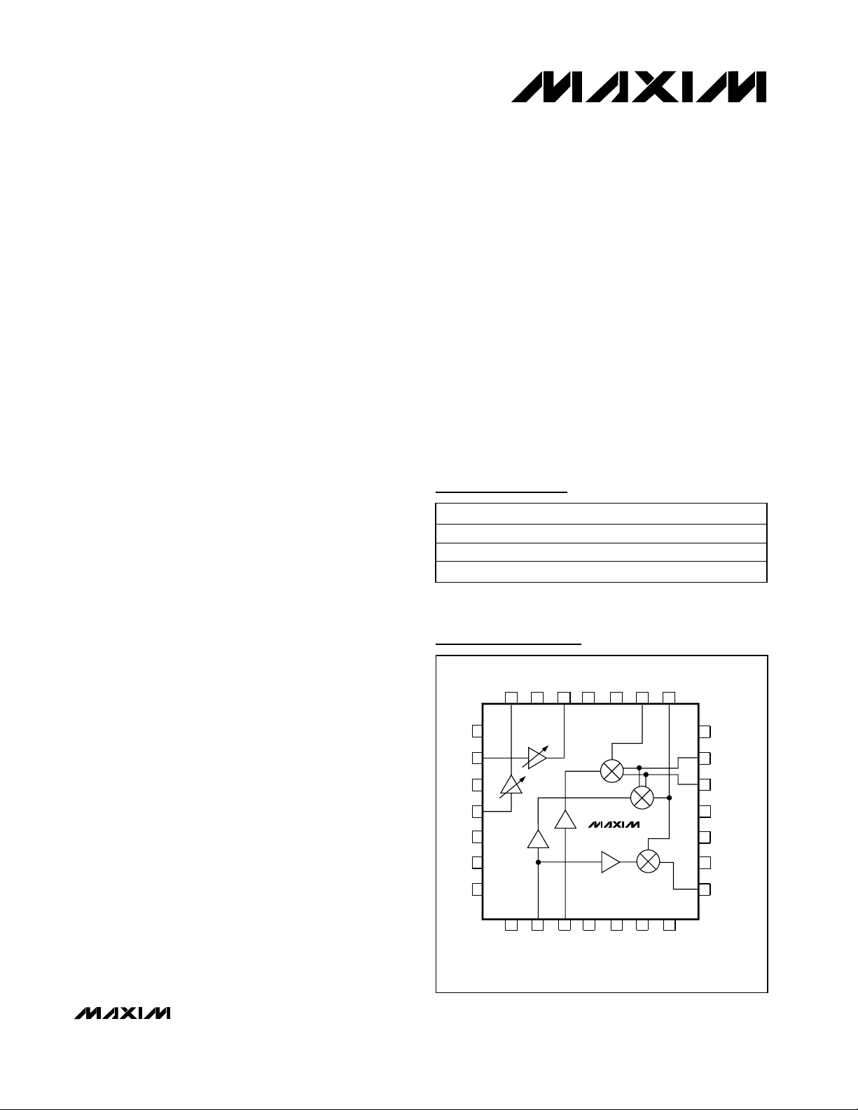
Pin Configuration/
Functional Diagram
Typical Application Circuits appear at end of data sheet.
T
Ordering Information
PART TEMP. RANGE PIN- PACKAGE
MAX2323EGI -40°C to +85°C 28 QFN
MAX2325EGI -40°C to +85°C
MAX2323EVKIT -40°C to +85°C
28 QFN
28 QFN
TOP VIEW
RLNA
PLNAIN
GND
CLNAIN
SLEEP
G2
G1
CLNAOU
GND
PLNAOUTGND
27
28 22
1
2
3
4
5
6
7
8
9
GND
LOLIN
2526
MAX2323
10 11 12 13 14
GND
LOHIN
QFN
GND
GND
2324
PMIXIN
GND
CMIXIN
MODE.
21
20
19
18
17
16
15
RBIAS
CDMA+
CDMA-
GND
BAND
V
CC
FMOUT
Page 2
MAX2323/MAX2325
Triple/Dual-Mode
CDMA LNA/Mixers
2 _______________________________________________________________________________________
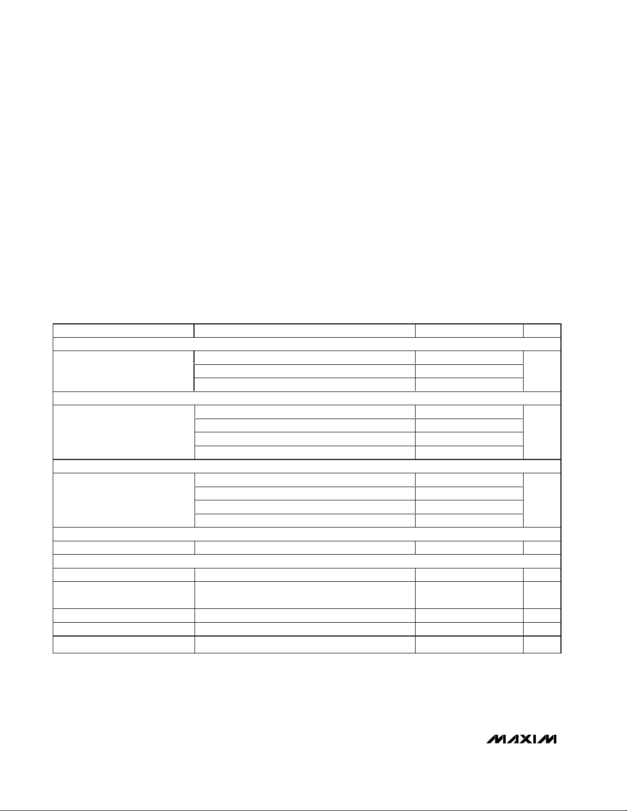
ABSOLUTE MAXIMUM RATINGS
DC ELECTRICAL CHARACTERISTICS
(VCC= +2.7V to +3.6V, R
RBIAS
= 20kΩ, R
RLNA
= 24kΩ, TA= -40°C to +85°C, no RF applied. Typical values are VCC= 2.75V and
T
A
= +25°C, unless otherwise noted.)
Stresses beyond those listed under “Absolute Maximum Ratings” may cause permanent damage to the device. These are stress ratings only, and functional
operation of the device at these or any other conditions beyond those indicated in the operational sections of the specifications is not implied. Exposure to
absolute maximum rating conditions for extended periods may affect device reliability.
VCCto GND ...............................................................0.3V, +4.3V
Digital Input Voltage to GND......................-0.3V to (V
CC
+ 0.3V)
LNA Input Level .....................................................................1Vp
LO, Mixer Input Levels .....................................................+5dBm
Digital Input Current .........................................................±10mA
Continuous Power Dissipation (T
A
= +70°C)
28-Pin QFN (derate 28.5mW/°C
above T
A
= +70°C) ...................................................2000mW
Operating Temperature Range ...........................-40°C to +85°C
Junction Temperature......................................................+150°C
Storage Temperature Range .............................-65°C to +150°C
Lead Temperature (soldering, 10s) ................................ +300°C
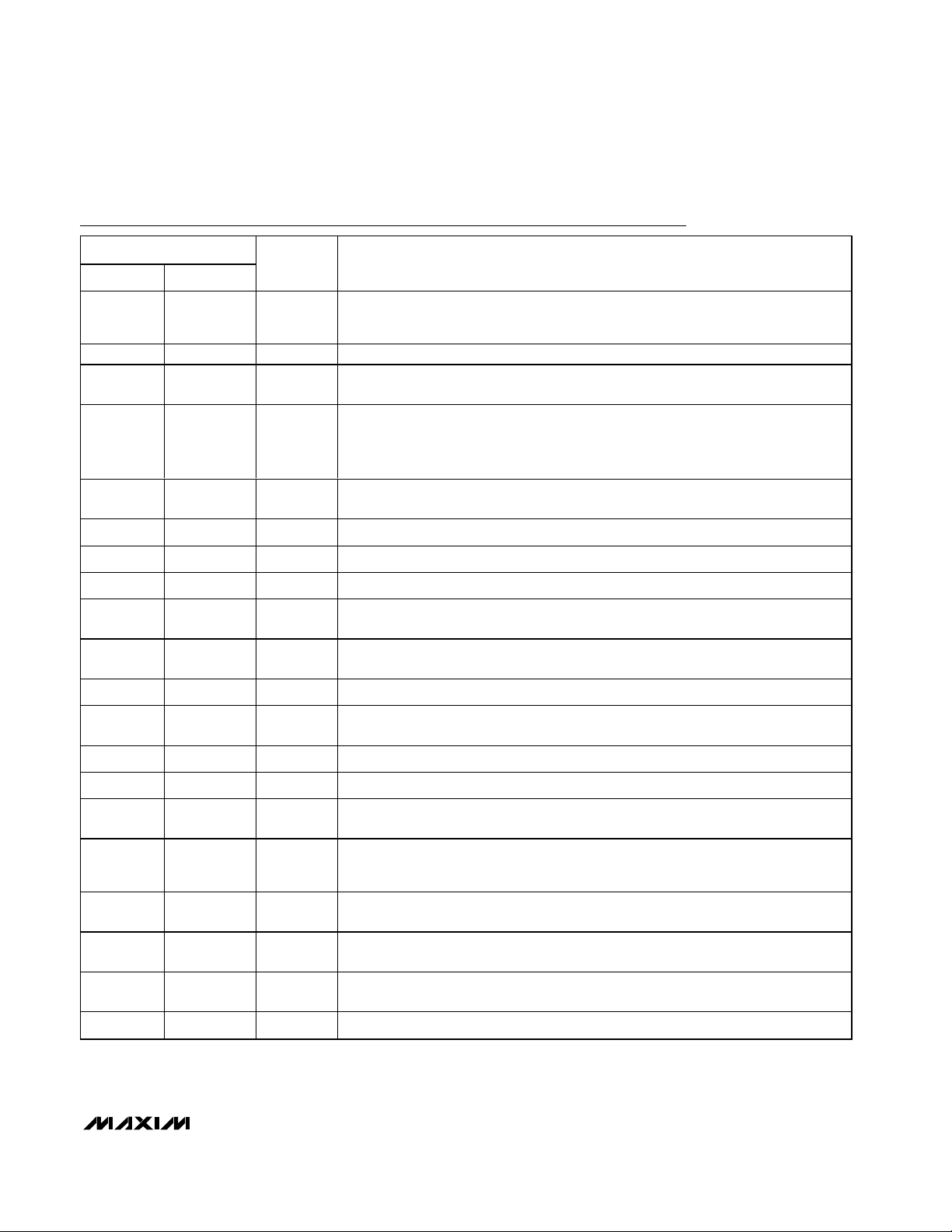
PCS CDMA MODE (MAX2323)
PARAMETER CONDITIONS MIN TYP MAX UNITS
CELLULAR CDMA MODE (MAX2323/MAX2325)
Operating Supply Current
FM MODE (MAX2323/MAX2325)
Operating Supply Current
SHUTDOWN MODE
Shutdown Supply Current SLEEP = high 1 25 µA
ALL MODES
Digital Input Logic High Except SLEEP input 2.0 V
SLEEP Input Logic High
Digital Input Logic Low 0.6 V
Digital Input Current High 5 µA
Digital Input Current Low -25 µA
Midgain mode 20.5 24
High-gain, low-linearity idle mode 22 25.5Operating Supply Current
High-gain, high-linearity mode 25.5 30
Low-gain mode 18.0 21.5
Midgain mode 19.5 23.5
High-gain, low-linearity idle mode 19.5 23.5
High-gain, high-linearity mode 26.5 31.5
Low-gain mode 15 18
Midgain mode 16.5 20
High-gain, low-linearity mode 16.5 20
High-gain, high-linearity mode 23.5 28
V
-
CC
0.6
mA
mA
mA
V
Page 3
MAX2323/MAX2325
Triple/Dual-Mode
CDMA LNA/Mixers
_______________________________________________________________________________________ 3
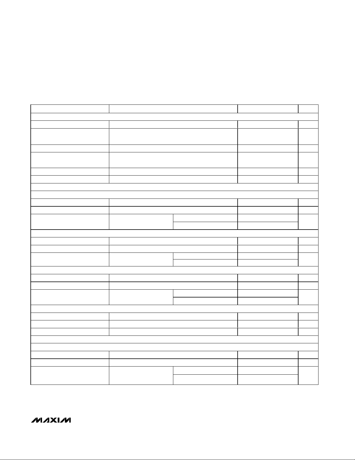
AC ELECTRICAL CHARACTERISTICS
(MAX2323 EV kit, F
PLNAIN
= 1960MHz, F
CLNAIN
= 881MHz, FIF= 110MHz, high-side LO, 50Ω system, R
RBIAS
= 20kΩ,
R
RLNA
= 24kΩ. Typical values are VCC= 2.75V, TA= +25°C. LO input power = -7dBm, LOW = 0V, HIGH = VCC, unless otherwise
noted.) (Note 1)
OVERALL PERFORMANCE
Low-Band RF Frequency Range (Note 2) 850 950 MHz
High-Band RF Frequency
Range
Low-Band LO Frequency Range (Note 2)
High-Band LO Frequency
Range
IF Frequency Range (Note 2) 40 400 MHz
LO Input Level 100Ω input impedance -7 -5 0 dBm
CELLULAR LNA PERFORMANCE (MAX2323/MAX2325)
CDMA AND FM HIGH-GAIN, HIGH-LINEARITY MODES
Gain TA = T
Noise Figure 1.7 1.9 dB
IIP3
CDMA HIGH-GAIN, LOW-LINEARITY PAGING MODE, AND FM HIGH-GAIN MODE
Gain TA = T
LNA Noise Figure 1.7 1.9 dB
LNA IIP3 (Note 3)
CDMA AND FM MIDGAIN MODES
Gain TA = T
Noise Figure 3.3 3.5 dB
IIP3 (Note 3)
CDMA AND FM LOW-GAIN MODES
Gain TA = T
Noise Figure 7.5 8.5 dB
IIP3 (Note 3) 13 17.5 dBm
PCS LNA PERFORMANCE (MAX2323)
CDMA HIGH-GAIN, HIGH-LINEARITY MODE
Gain TA = T
Noise Figure 1.9 2.1 dB
IIP3 (Note 3)
PARAMETER CONDITIONS MIN TYP MAX UNITS
MAX2323 (Note 2) 1800 2200 MHz
MAX2323 (Note 2) 1600 2300 MHz
MIN
MIN
MIN
MIN
MIN
800 1150 MHz
to T
to T
to T
to T
to T
MAX
MAX
MAX
MAX
MAX
TA = +25°C 9 10.5
= T
= T
= T
= T
MIN
MIN
MIN
MIN
to T
to T
to T
to T
MAX
MAX
MAX
MAX
T
A
TA = +25°C 2.5 5
T
A
TA = +25°C 8.5 10
T
A
TA = +25°C78
T
A
14.5 15.5 17 dB
7.5
13 14.5 16 dB
2.7
4.5 6 8 dB
5
-4.5 -3.5 -1.5 dB
13.5 14.5 15.5 dB
5.5
dBm
dBm
dBm
dBm
Page 4
Note 1: Devices are production tested for functionality at frequencies stated; 30 units from 3 independent wafer lots, when one lot
was at the upper process extreme, one lot was nominal, and one lot was at the lower process extreme, were characterized.
The resulting standard deviation therefore includes process variations. Data sheet limits are ±3σ from the mean.
Note 2: Operation over this frequency range requires the ports to be rematched for the desired operating range. Performance at
various frequencies is indicated by the S-parameter data in Tables 3–7.
Note 3: Specifications are based on R
BIAS
= 20kΩ. ICCfor all LNAs (except HGHL) and mixers are inversely proportional to R
RBIAS
.
IIP3 can be traded for I
CC
by selecting other values of R
RBIAS
.
MAX2323/MAX2325
Triple/Dual-Mode
CDMA LNA/Mixers
4 _______________________________________________________________________________________
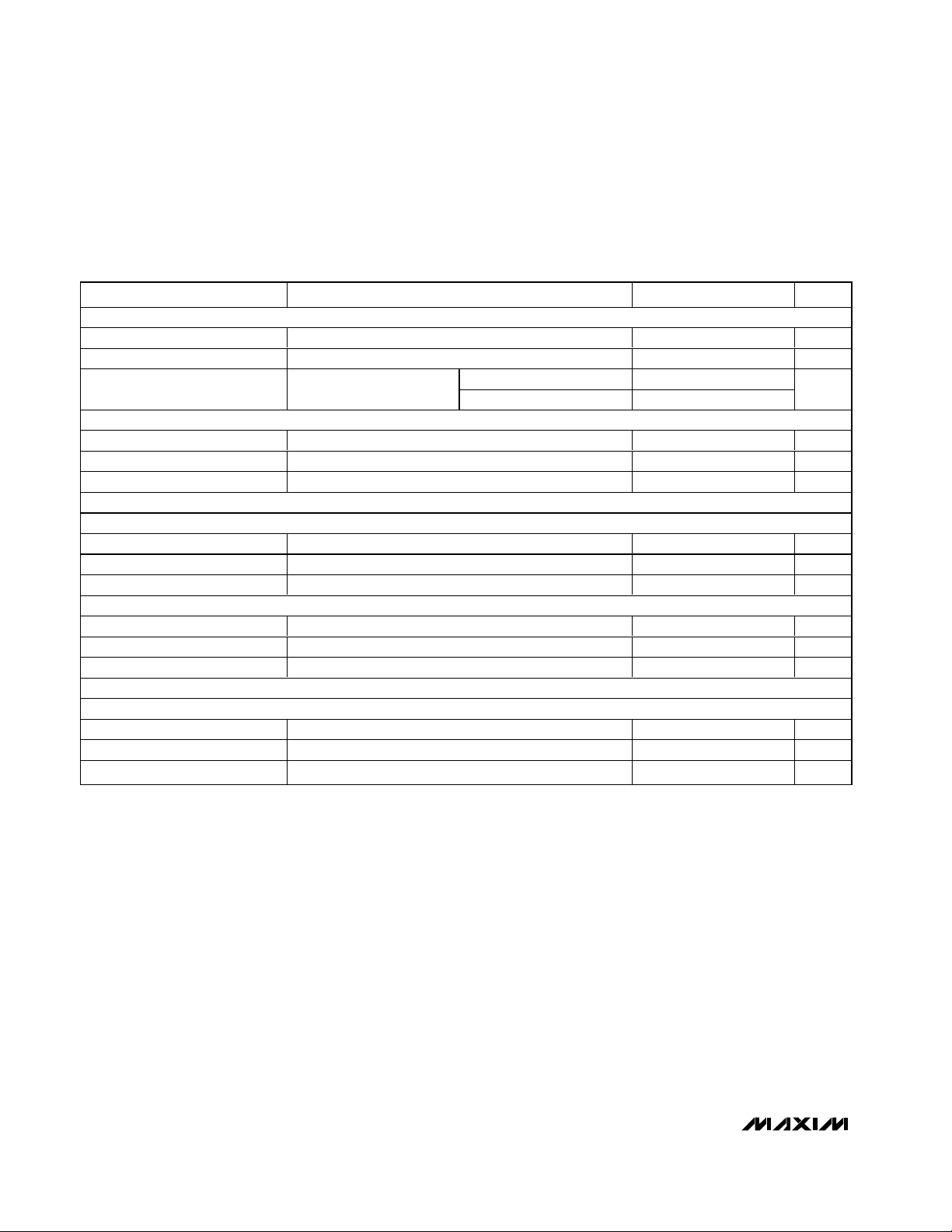
AC ELECTRICAL CHARACTERISTICS (continued)
(MAX2323 EV kit, F
PLNAIN
= 1960MHz, F
CLNAIN
= 881MHz, FIF= 110MHz, high-side LO, 50Ω system, R
RBIAS
= 20kΩ,
R
RLNA
= 24kΩ. Typical values are VCC= 2.75V, TA= +25°C. LO input power = -7dBm, LOW = 0V, HIGH = VCC, unless otherwise
noted.) (Note 1)
CDMA HIGH-GAIN, LOW-LINEARITY PAGING MODE
Gain TA = T
LNA Noise Figure 1.9 2.1 dB
LNA IIP3 (Note 3)
CDMA MIDGAIN MODE
Gain TA = T
Noise Figure 5.6 6.0 dB
IIP3 (Note 3)
CELLULAR MIXER PERFORMANCE (MAX2323/MAX2325)
CDMA, ALL MODES
Gain TA = T
Noise Figure 7.5 8.5 dB
IIP3 TA = T
FM MODE
Gain TA = T
Noise Figure 10.5 11.5 dB
IIP3 TA = T
PCS MIXER PERFORMANCE (MAX2323)
CDMA HIGH-GAIN, HIGH-LINEARITY MODE
Gain TA = T
Noise Figure 7.9 8.5 dB
IIP3 TA = T
PARAMETER CONDITIONS MIN TYP MAX UNITS
to T
MIN
to T
MIN
to T
MIN
to T
MIN
to T
MIN
to T
MIN
to T
MIN
to T
MIN
MAX
TA = +25°C
T
= T
MIN
to T
MAX
A
MAX
MAX
(Note 3) 3.5 4.8 dBm
MAX
MAX
(Note 3) 1.5 5 dBm
MAX
MAX
(Note 3) 1.5 4 dBm
MAX
12.5 14 14.5 dB
4.5 5.5
3.0
-2.0 -1.0 -0.5 dB
12 13.5 dBm
11.5 13 14.5 dB
8.5 10 11.5 dB
12 13.5 15.5 dB
dBm
Page 5
MAX2323/MAX2325
Triple/Dual-Mode
CDMA LNA/Mixers
_______________________________________________________________________________________ 5
Pin Description
PIN
MAX2323 MAX2325
1 1 RLNA
— 2, 10, 23 N.C. No Connection. Leave this pin floating.
2 — PLNAIN
3, 8, 11,
12, 13, 18,
24, 25, 27
4 4 CLNAIN
5 5 SLEEP Logic Input. High shuts off entire device.
6 6 G2 Logic Input. See Tables 1 and 2 for details.
7 7 G1 Logic Input. See Tables 1 and 2 for details.
9 9 LOLIN
10 — LOHIN
14 14 MODE Logic Input. See Tables 1 and 2 for details.
15 15 FMOUT
16 16 V
17 — BAND Logic Input. High selects high band (PCS). Low selects low band (cellular).
19, 20 19, 20
21 21 RBIAS
22 22 CMIXIN
23 — PMIXIN
26 — PLNAOUT
—
3, 8, 11, 12,
13, 17, 18,
24, 25, 27
26
NAME FUNCTION
L N A B i a s - S e t t i ng P i n . F o r no m i n a l b i a s , c o n n ec t a 24 k Ω r es i s t o r t o g r o u n d . T h i s
r e si s t o r v a l u e c a n b e a d j u st e d t o a l t e r t h e l i n e a r i t y o f t h e i np u t L N A i n hi g h - g ai n ,
h i g h - l i n ea r i t y C D M A m o d e s .
High-Band RF Input Port. Blocking capacitor is required, which may be used as part of
the matching network.
GND Ground
Low-Band RF Input Port. Blocking capacitor is required, which may be used as part of
the matching network.
Low-Frequency LO Input Port. Requires blocking capacitor, which may be used as
part of an optional matching network.
High-Frequency LO Input Port. Requires blocking capacitor, which may be used as
part of an optional matching network.
FM IF Output Port. Requires a pull-up inductor and a DC blocking capacitor, which
may be used as part of the matching network.
CC
CDMA-,
CDMA+
V
CC
2.7V to 3.6V Supply Pin. Must be capacitively bypassed near the pin.
Differential Output Port for CDMA Mode. Requires pull-up inductors and blocking
capacitors, which may be used as part of the matching network.
Bias Setting Pin. For nominal bias, connect a 20kΩ resistor to ground. This resistor
value can be adjusted to alter the linearity of the mixers in all modes and the LNA in all
modes except high gain and high linearity.
Low-Band Mixer Input Port. Requires blocking capacitor, which may be used as part of
the matching network.
High-Band Mixer Input Port. Requires blocking capacitor, which may be used as part
of the matching network.
High-Band LNA Output Port. This port requires an external pull-up inductor and series
capacitor as part of the matching network.
2.7 to 3.6V Supply Pin. Bypassing is not necessary at this pin.
Page 6

MAX2323/MAX2325
Triple/Dual-Mode
CDMA LNA/Mixers
6 _______________________________________________________________________________________
Pin Description (continued)
Table 1. MAX2323 Operational Modes
X: Don’t care
MAX2323 MAX2325 NAME FUNCTION
28 28 CLNAOUT
Slug Slug GND Ground
MODES
BAND
PCS Band, High Gain,
High Linearity (HGHL)
PCS Band, High Gain,
Low Linearity (Paging
Mode) (HGLL)
PCS Band, Midgain
(MGHL)
Cellular Band CDMA
Mode, High Gain, High
Linearity (HGHL)
P √√1X 00 0
P √√1X 01 0
P √√ 1X 100
C √√01 000
Low-Band LNA Output Port. This port requires an external pull-up inductor and series
capacitor as part of the matching network.
FUNCTION CTRL PIN
HGHL AMP
HGLL AMP
MGHL AMP
LGHL AMP
CDMA MIXER
FM MIXER
BAND
MODE
G1
G2
SLEEP
Cellular Band CDMA,
High Gain, Low Linearity
(Paging Mode) (HGLL)
Cellular Band, CDMA
Mode, Midgain (MGHL)
Cellular Band, CDMA
Mode, Low Gain (LGHL)
Cellular Band, FM Mode,
High Gain, Low Linearity
(HGLL)
Cellular Band, FM Mode,
Midgain
Cellular Band, FM Mode,
Low Gain
Shutdown — —— ———— XX XX 1
Undefined ——————— 1X11 0
Cellular Band, FM Mode,
High Gain, High Linearity
(HGHL)
C √√01 010
C √√ 01 100
C √√ 01 110
C √√00 01 0
C √√00 10 0
C √√00 11 0
C √ ———— √ 0000 0
Page 7

MAX2323/MAX2325
Triple/Dual-Mode
CDMA LNA/Mixers
_______________________________________________________________________________________ 7
Table 2. MAX2325 Operational Modes
X: Don’t care
FUNCTION CTRL PIN
MODES
BAND
Cellular Band CDMA
Mode, High Gain, High
Linearity (HGHL)
Cellular Band CDMA,
High Gain, Low Linearity
(Paging Mode) (HGLL)
Cellular Band, CDMA
Mode, Midgain (MGHL)
Cellular Band, CDMA
Mode, Low Gain (LGHL)
Cellular Band, FM Mode,
High Gain, Low Linearity
(HGLL)
Cellular Band, FM Mode,
Midgain
Cellular Band, FM Mode,
Low Gain
Shutdown ——————— XXX1
C √√1000
C √√1010
C √√1100
C √√ 1110
C √√0010
C √√0100
C √√0110
HGHL AMP
HGLL AMP
MGHL AMP
LGHL AMP
CDMA MIXER
FM MIXER
MODE
G1
G2
SLEEP
Cellular Band, FM Mode,
High Gain, High Linearity
(HGHL)
√√0000
Page 8

MAX2323/MAX2325
Triple/Dual-Mode
CDMA LNA/Mixers
8 _______________________________________________________________________________________
Table 3. Cellular LNA S Parameters in High-Gain High-Linearity Mode
Table 4. PCS LNA S Parameters in High-Gain High-Linearity Mode
FREQUENCY
(MHz)
700 0.623 -81.9 4.58 79.8 0.046 59.5 0.746 -29.5
750 0.627 -84.3 4.30 78.0 0.048 60.6 0.748 -30.2
800 0.629 -86.6 4.06 74.8 0.049 60.9 0.750 -30.9
850 0.631 -89.0 3.70 72.3 0.051 61.4 0.749 -31.1
900 0.632 -91.4 3.50 72.2 0.052 62.1 0.751 -32.3
950 0.635 -93.7 3.39 68.7 0.053 61.3 0.753 -33.0
1000 0.635 -96.0 3.08 66.3 0.053 62.7 0.753 -33.5
FREQUENCY
(MHz)
1700 0.671 -125.8 5.77 109.2 0.062 90.4 0.796 -50.3
S11
(MAG)
S11
(MAG)
S11
(PHASE)
S11
(PHASE)
S21
(MAG)
S21
(MAG)
S21
(PHASE)
S21
(PHASE)
S12
(MAG)
S12
(MAG)
(PHASE)
(PHASE)
S12
S12
S22
(MAG)
S22
(MAG)
S22
(PHASE)
S22
(PHASE)
1750 0.675 -126.9 5.66 109.3 0.064 89.9 0.800 -50.7
1800 0.685 -128.9 5.66 107.2 0.065 89.1 0.808 -51.7
1850 0.689 -130.8 5.56 106.3 0.066 88.7 0.812 -52.6
1900 0.694 -132.7 5.63 104.7 0.066 89.3 0.817 -53.6
1950 0.696 -134.3 5.54 102.7 0.066 90.6 0.820 -54.4
2000 0.700 -135.8 5.50 101.2 0.068 91.9 0.826 -55.3
2050 0.706 -137.3 5.41 99.0 0.070 92.6 0.832 -56.3
2100 0.712 -138.9 5.33 97.4 0.072 92.7 0.839 -57.4
2150 0.717 -140.4 5.24 95.0 0.073 93.0 0.844 -58.8
2200 0.718 -141.9 5.08 93.3 0.073 94.2 0.845 -60.1
2250 0.721 -143.2 4.99 91.2 0.074 96.2 0.849 -61.4
2300 0.724 -144.5 4.78 89.0 0.077 98.3 0.852 -62.9
2350 0.730 -145.6 4.64 87.7 0.081 99.2 0.858 -64.5
2400 0.735 -146.9 4.45 85.7 0.085 99.4 0.862 -66.5
2450 0.740 -147.9 4.33 85.4 0.087 99.3 0.867 -68.0
2500 0.746 -148.4 4.39 85.5 0.089 99.5 0.875 -69.1
Page 9

MAX2323/MAX2325
Triple/Dual-Mode
CDMA LNA/Mixers
_______________________________________________________________________________________ 9
Table 5. Cellular Mixer S11 in High-Gain
High-Linearity Mode
Table 6. PCS Mixer S11 in High-Gain
High-Linearity Mode
FREQUENCY
(MHz)
700 0.803 -17.5
750 0.792 -18.1
800 0.799 -18.8
850 0.769 -20.2
900 0.761 -21.9
950 0.751 -23.9
1000 0.738 -26.7
S11
(MAG)
S11
(PHASE)
FREQUENCY
(MHz)
1700 0.764 -42.6
1750 0.763 -44.1
1800 0.764 -45.8
1850 0.763 -47.3
1900 0.765 -48.5
1950 0.762 -50.0
2000 0.762 -50.1
2050 0.762 -50.0
2100 0.762 -49.9
2150 0.762 -49.9
2200 0.762 -50.0
2250 0.762 -50.0
2300 0.762 -49.9
2350 0.762 -50.1
S11
(MAG)
S11
(PHASE)
2400 0.751 -64.4
2450 0.750 -64.3
2500 0.750 -64.2
Page 10

MAX2323/MAX2325
Triple/Dual-Mode
CDMA LNA/Mixers
10 ______________________________________________________________________________________
Table 7. Mixer IF Port S22
FREQUENCY
(MHz)
50 0.999 -2.1 50 0.998 -1.7
100 0.997 -4.1 70 0.998 -2.5
110 0.996 -4.5 85 0.998 -2.8
130 0.995 -5.5 100 0.998 -3.6
150 0.994 -6.2 110 0.998 -4.0
200 0.993 -8.2 150 0.998 -5.4
210 0.992 -8.6 200 0.998 -7.2
250 0.986 -10.0 250 0.997 -8.9
300 0.983 -12.0 300 0.997 -10.6
350 0.982 -13.9 350 0.997 -12.1
400 0.977 -15.8 400 0.997 -13.8
DIGITAL MIXER
(SINGLE-ENDED)
S22
(MAG)
S22
(PHASE)
FREQUENCY
(MHz)
S22
(MAG)
FM MIXER
S22
(PHASE)
Page 11

MAX2323/MAX2325
Triple/Dual-Mode
CDMA LNA/Mixers
______________________________________________________________________________________ 11
Typical Application Circuits
PCS
CELLULAR
SLEEP
CELLULAR
V
CC
PCS
27
28 22
1
2
3
4
5
2526
MAX2323
2324
21
20
19
18
17
BAND
V
CC
CDMA
V
CC
G2
G1
CELLULAR LO
PCS LO
6
7
8
10 11 12 13 14
9
16
FM
15
MODE
Page 12

MAX2323/MAX2325
Triple/Dual-Mode
CDMA LNA/Mixers
12 ______________________________________________________________________________________
Typical Application Circuits (continued)
V
CC
27
28 22
1
SLEEP
2
3
4
5
G2
6
G1
7
8
9
VCO
2526
2324
MAX2325
10 11 12 13 14
MODE
V
CC
21
20
19
18
17
16
15
CDMA
V
CC
FM
Page 13

MAX2323/MAX2325
Triple/Dual-Mode
CDMA LNA/Mixers
______________________________________________________________________________________ 13______________________________________________________________________________________ 13
Component List
EV Kit Information
DESIGNATION QTY DESCRIPTION
C1, C4, C9,
C24, C29
C2, C3,
C21, C22, C27
C17 1
C7 1
C8 1
C12 1 0Ω resistor (0402)
C6, C10 — Not installed
C11, C18, C19,
C26, C28,
C32, C33
C5, C14, C16 3
C15 1
C23, C25 2
C31 1
L1 1
L2, L4 2
L3, L6 2 0Ω resistors (0603)
L5 1
0.01µF ±10% ceramic caps (0402)
Murata GRM36X7R103K016 or
5
Taiyo Yuden EMK105B103KW
100pF ±5% ceramic caps (0402)
Murata GRM36COG101J050 or
5
Taiyo Yuden UMK105CH101JW
2.7pF ±0.1pF ceramic cap (0402)
Murata GRM36COG2R7B050 or
Taiyo Yuden EVK105CH2R7JW
3.0pF ±0.1pF ceramic cap (0402)
Murata GRM36COG3R0B050 or
Taiyo Yuden EVK105CH3R0JW
1.5pF ±0.1pF ceramic cap (0402)
Murata GRM36COG1R5B050 or
Taiyo Yuden EVK105CH1R5BW
1000pF ±10% ceramic caps (0402)
Murata GRM36X7R102K050 or
7
Taiyo Yuden UMK105B102KW
6800pF ±10% capacitors (0402)
Murata GRM36X7R682K025 or
Taiyo Yuden TMK105B682KW
1.0pF ±0.1pF ceramic cap (0402)
Murata GRM36COG010B050 or
Taiyo Yuden EVK105CH010BW
5.6pF ±0.25pF ceramic caps (0402)
Murata GRM36COG5R6C050
4.3pF ±0.1pF ceramic cap (0402)
Murata GRM36COG4R3B050 or
Taiyo Yuden EVK105CH4R3JW
8.2nH ±5% inductor (0603)
Murata LQG11A8N2J00
1.8nH ±10% inductors (0603)
Coilcraft 0603CS-1N8XKBC
6.8nH ±5% inductor (0603)
Murata LQG11A6N8J00
DESIGNATION QTY DESCRIPTION
L7, L8 2
L10 1
L11 1
L12 1
R1, R4, R5,
R8, R10
R2 1 24.3kΩ ±1% resistor (0402)
R3 1 20.0kΩ ±1% resistor (0402)
R7 1 2.7kΩ ±5% resistor (0402)
R11 1 8.2kΩ ±5% resistor (0402)
T1 1
PLNAIN,
CLNAIN,
LOLIN, LOHIN,
CLNAOUT,
PLNAOUT,
CDMAOUT,
FMOUT
PMIXIN,
CMIXIN
GND, VCC 2
JU1, JU3, JU4,
JU7, JU9
JU2, JU6, JU8,
JU10
None 10 Shunts (JU1–JU4, JU6–JU10)
U1 1 MAX2323EGI (QFN-28)
None 1 MAX2323/MAX2325 data sheet
None 1 MAX2323 PC board
51kΩ ±5% resistors (0402)
8
2
5 3-pin headers
4 2-pin headers
270nH ±2% inductors (0805)
Coilcraft 0805CS-271XGBC
3.9nH ±0.3nH inductor (0603)
Murata LQG11A3N9S00
330nH ±2% inductor (0805)
Coilcraft 0805CS-331XGBC
2.7nH ±0.3nH inductor (0603)
Murata LQG11A2N7S00
Balun transformer (B5F type)
Toko 458DB-1011
SMA connectors (PC edge mount)
EFJohnson 142-0701-801 or
Digi-Key J502-ND
SMA connectors (vertical mount)
Digi-Key J500-ND
Test points
Mouser 151-203
Page 14

MAX2323/MAX2325
Triple/Dual-Mode
CDMA LNA/Mixers
MAX2323
U1
CLNAOUT
RLNA
PLNAIN
GND
CLNAIN
SLEEP
G2
G1
RBIAS
IF+
IF-
GND
BAND
V
CC
FM
GND PLNAOUT GND GND PMIXIN CMIXIN
GND LOLIN LOHIN GND GND GND MODE
JU2
C2
100pF
L1
8.2nH
L4
1.8nH
C7
3.0pF
R2
24.3k
SMA
CLNAOUT
SMA
PLNAIN
C1
0.01µF
V
CC
JU10
C3
100pF
L2
1.8nH
C4
0.01µF
V
CC
C14
6800pF
SMA
CLNAIN
C16
6800pF
C15
1.0pF
L5
6.8nH
C17
2.7pF
C11
1000pF
JU1
V
CC
R1
1k
C18
1000pF
C27
100pF
C26
1000pF
C28
1000pF
C29
0.01µF
JU3
V
CC
R4
1k
C19
1000pF
JU4
V
CC
R5
1k
SMA
LOLIN
C21
100pF
SMA
LOHIN
C22
100pF
R10
1k
JU9
V
CC
C32
1000pF
SMA
FMOUT
JU8
L11
330nH
V
CC
R11
8.2k
R7
2.7k
C33
1000µF
C31
4.3pF
V
CC
GND
V
CC
JU7
V
CC
R8
1k
JU6
V
CC
L7
270nH
C24
0.01µF
C23
5.6pF
C25
5.6pF
L8
270nH
3
2
1
4
6
SMA
CDMAOUT
T1
458DB-1011
R3
20k
L6
0Ω
SMA
CMIXIN
L10
3.9nH
C10
OPEN
C9
0.01µF
L3
0Ω
SMA
PMIXIN
L12
2.7nH
C6
OPEN
C5
6800pF
SMA
PLNAOUT
C8
1.5pF
1
2
3
4
5
6
7
8 9 10 11 12 13 14
15
16
17
18
19
20
21
22232425262728
C12
0Ω
L9
OPEN
L12 POSITION: 1mm FROM C5
Figure 1. MAX2323 Evaluation Kit
Maxim cannot assume responsibility for use of any circuitry other than circuitry entirely embodied in a Maxim product. No circuit patent licenses are
implied. Maxim reserves the right to change the circuitry and specifications without notice at any time.
14 ____________________Maxim Integrated Products, 120 San Gabriel Drive, Sunnyvale, CA 94086 408-737-7600
© 2000 Maxim Integrated Products Printed USA is a registered trademark of Maxim Integrated Products.
Package Information
For the latest package outline information, go to
www.maxim-ic.com/packages.
 Loading...