Page 1

General Description
The MAX2203 RMS power detector is designed to
operate from 800MHz to 2.0GHz. The device is ideal for
wideband code-division multiple access (WCDMA),
cdma2000
®
, and high-speed downlink/uplink packet
access. The MAX2203 accepts an RF signal at the
input and outputs the same voltage regardless of the
peak-average of the input signal. The output voltage
and input power is linear in dB. The device has a
-24dBm to +3dBm detection range, and every dB
change in input power gives 35mV (typ) change in output voltage.
The MAX2203 operates from a 2.5V to 4.2V supply and
is specified over the -40°C to +85°C extended temperature range. The device is available in a 6-bump WLP
package.
Applications
WCDMA, cdma2000, 1xEVDO
High-Speed Downlink Packet Access (HSDPA)
High-Speed Uplink Packet Access (HSUPA)
Features
o -24dBm to +3dBm Power-Detection Range
o 35mV/dB (typ) Log Detector
o 0.1dB (typ) RMS Accuracy from WCDMA
Modulation Change
o ±0.4dB Detection Error Due to Temperature
o +2.5V to +4.2V Single-Supply Operation
o Space-Saving 6-Bump WLP Package
MAX2203
RMS Power Detector
________________________________________________________________
Maxim Integrated Products
1
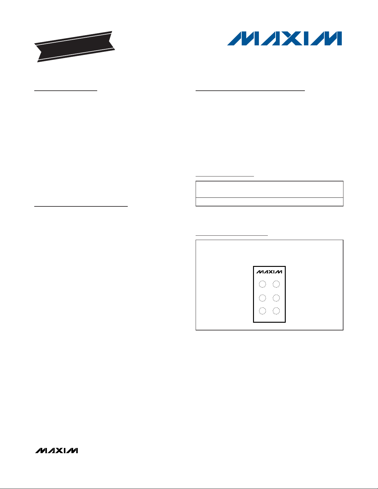
Pin Configuration
Ordering Information
19-4982; Rev 0; 10/09
For pricing, delivery, and ordering information, please contact Maxim Direct at 1-888-629-4642,
or visit Maxim’s website at www.maxim-ic.com.
EVALUATION KIT
AVAILABLE
PART TEMP RANGE
PIN-
PACKAGE
TOP
MARK
MAX2203EWT+T10 -40°C to +85°C 6 WLP AA
+
Denotes a lead(Pb)-free/RoHS-compliant package.
T = Tape and reel.
Typical Operating Circuit appears at end of data sheet.
cdma2000 is a registered trademark of Telecommunications
Industry Association.
TOP VIEW
(BUMPS ON BOTTOM)
12
+
MAX2203
A
RFIN/ENA
GND
B
GND
FILT
C
V
OUT
CC
Page 2

MAX2203
RMS Power Detector
2 _______________________________________________________________________________________
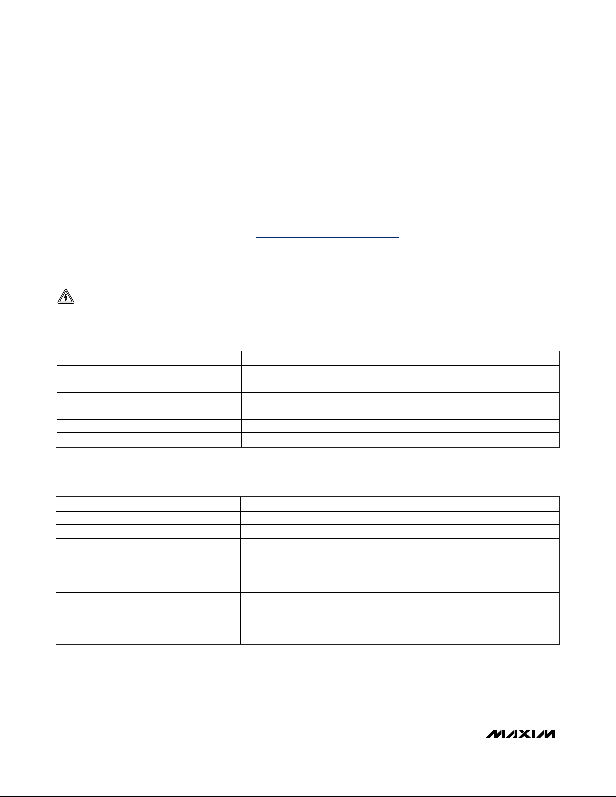
ABSOLUTE MAXIMUM RATINGS
DC ELECTRICAL CHARACTERISTICS
(VCC= 2.5V to 4.2V, TA= -40°C to +85°C, V
ENA
= 2.7V, no RF signal applied. Typical values are at VCC= 2.8V, TA= +25°C, unless
otherwise noted.) (Note 3)
Stresses beyond those listed under “Absolute Maximum Ratings” may cause permanent damage to the device. These are stress ratings only, and functional
operation of the device at these or any other conditions beyond those indicated in the operational sections of the specifications is not implied. Exposure to
absolute maximum rating conditions for extended periods may affect device reliability.
Note 3: Guaranteed by production test at TA= +85°C and 800MHz. Guaranteed by design and characterization at TA= -40°C and
T
A
= +25°C, and over frequency limits.
Note 4: Guaranteed by design and characterization.
Note 5: Input power -24dBm to +3dBm. Ideal straight line calibrated with input power -20dBm and 0dBm at T
A
= +25°C.
V
CC
to GND...........................................................-0.3V to +4.5V
ENA, OUT, FILT to GND ........................................-0.3V to +3.0V
RFIN Input Power ...........................................................+10dBm
Continuous Power Dissipation (TA= +70°C)
6-Bump WLP (derate 2.9mW/°C above +70°C)...........232mW
Junction-to-Ambient Thermal Resistance (θJA)
(Note 1) ......................................................................347°C/W
Operating Temperature Range ...........................-40°C to +85°C
Storage Temperature Range .............................-65°C to +160°C
Junction Temperature .....................................................+150°C
Lead Temperature (soldering, 10s)..........Reflow Profile (Note 2)
AC ELECTRICAL CHARACTERISTICS
(VCC= 2.8V, TA= -40°C to +85°C, V
ENA
= 2.7V, fRF= 800MHz to 2GHz, unless otherwise noted. Typical values are at TA= +25°C.)
(Note 3)
Note 1: Package thermal resistances were obtained using the method described in JEDEC specifications. For detailed information
on package thermal considerations, refer to www.maxim-ic.com/thermal-tutorial
.
Note 2: Refer to Application Note 1891:
Wafer-Level Packaging (WLP) and Its Applications
.
CAUTION! ESD SENSITIVE DEVICE
Supply Voltage V
Supply Current I
Shutdown Supply Current V
ENA Logic-High Threshold V
ENA Logic-Low Threshold V
ENA Input Current V
PARAMETER SYMBOL CONDITIONS MIN TYP MAX UNITS
CC
CC
VCC = 2.8V, RF input = -24dBm to +3dBm 5 8 mA
= 0V 0.5 10 µA
ENA
IH
IL
= 1.1V 25 µA
ENA
2.5 2.8 4.2 V
1.1 2.7 V
0 0.6 V
RF Input Frequency 800 2000 MHz
Max imum Output Voltage RFIN at +3dBm 1.05 1.5 1.75 V
Min imum Output Voltage No RF input power 300 400 mV
Minimum Input Power Level
Log Slope [(V
Log Conformance Error with
10dB Step
Power-Detector Accuracy Due to
Temperature
PARAMETER SYMBOL CONDITIONS MIN TYP MAX UNITS
+1dB input power step results in at least
25mV increase in V
at +3dBm) - (V
OUT
(Notes 4, 5) -1.3 +1.3 dB
RF input at -4dBm to 0dBm, TA = -40°C to
+85°C, relative to +25°C
(Note 4)
OUT
at -24dBm)]/27 25 35 45 mV/dB
OUT
-24 dBm
±0.4 dB
Page 3

MAX2203
RMS Power Detector
_______________________________________________________________________________________ 3
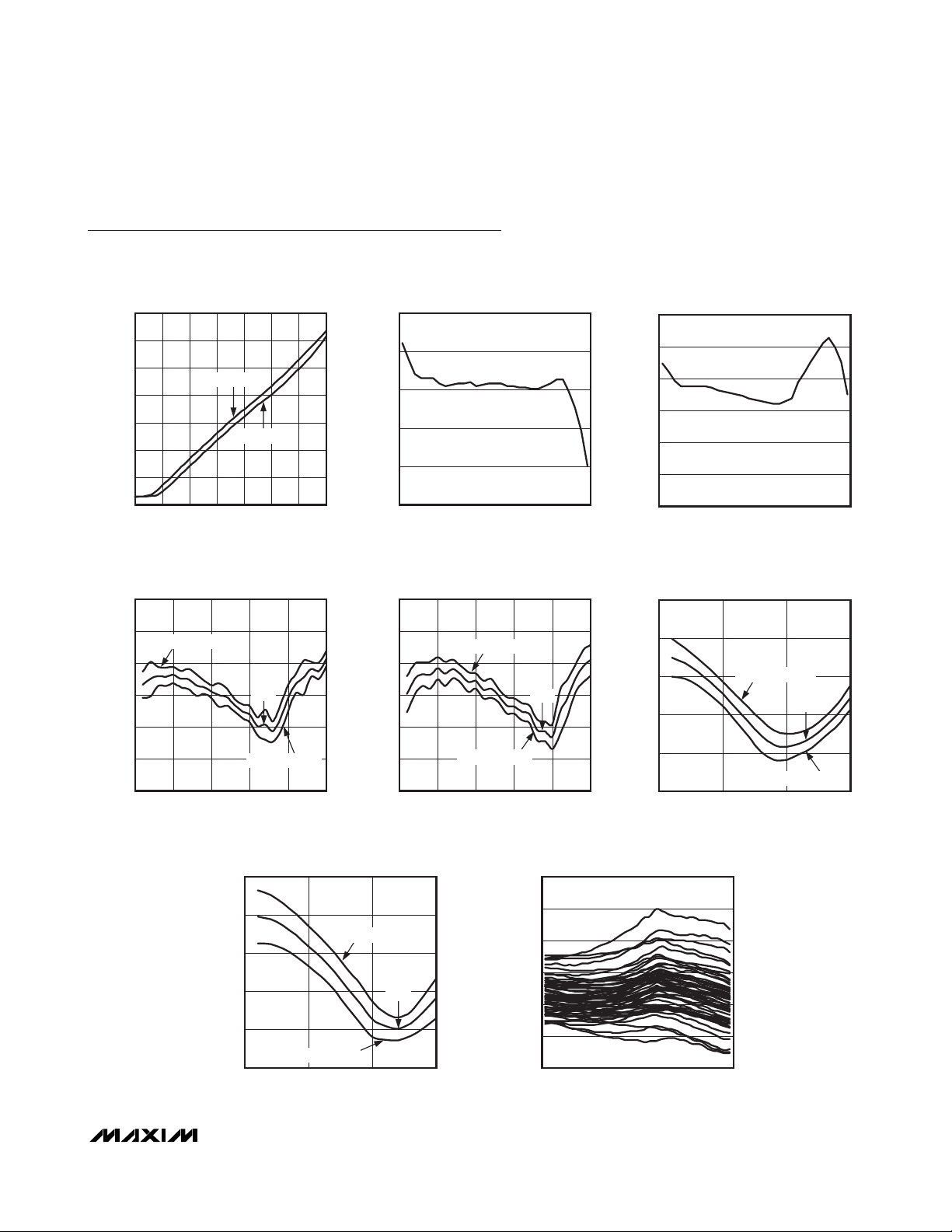
Typical Operating Characteristics
(VCC= 2.7V, TA= +25°C, WCDMA uplink DPCCH + 1DPDCH, log conformance calculation is referenced to a straight line that is
calibrated at -20dBm and 0dBm, unless otherwise noted.)
OUTPUT VOLTAGE vs. INPUT POWER
1.6
1.4
1.2
1.0
0.8
OUTPUT VOLTAGE (V)
0.6
0.4
0.2
-30 5
800MHz
2000MHz
INPUT POWER (dBm)
MAX2203 toc01
0-5-10-15-20-25
LOG CONFORMANCE WITH 1dB STEP
CELLULAR BAND
0.3
0.2
MEAN + 3 x STDEV
0.1
0
-0.1
LOG CONFORMANCE (dB)
-0.2
-0.3
MEAN
MEAN - 3 x STDEV
-5-10-15-20-25 0
INPUT POWER (dBm)
MAX2203 toc04
PCS WCDMA 1+1 vs. 1+5 RMS ERROR
(± DEVIATION FROM MIDPOINT)
0.25
0.20
0.15
0.10
RMS ERROR (dB)
0.05
0
-25
-21
-17
-13
-23
-19
-15
PIN (dBm)
-11 -7 -3
-9 -51-153
LOG CONFORMANCE WITH
1dB STEP PCS BAND
0.3
0.2
0.1
0
-0.1
LOG CONFORMANCE (dB)
-0.2
-0.3
MEAN + 3 x STDEV
MEAN - 3 x STDEV
INPUT POWER (dBm)
MEAN
-5-10-15-20-25 0
0.06
0.05
MAX2203 toc02
0.04
0.03
RMS ERROR (dB)
0.02
0.01
0
1.0
MAX2203 toc05
0.6
0.2
-0.2
LOG CONFORMANCE (dB)
-0.6
-1.0
-15 0
CELL WCDMA 1+1 vs. 1+5 RMS ERROR
(± DEVIATION FROM MIDPOINT)
-25
-21
-17
-13
-23
-19
-15
PIN (dBm)
-11 -7 -3
-9 -51-153
LOG CONFORMANCE WITH
10dB STEP CELLULAR BAND
MEAN + 3 x STDEV
MEAN
MEAN - 3 x STDEV
-5-10
INPUT POWER (dBm)
MAX2203 toc03
MAX2203 toc06
LOG CONFORMANCE WITH
10dB STEP PCS BAND
1.0
0.6
MEAN + 3 x STDEV
0.2
-0.2
LOG CONFORMANCE (dB)
-0.6
-1.0
-15 0
MEAN - 3 x STDEV
-5-10
INPUT POWER (dBm)
MAX2203 toc07
MEAN
TEMPERATURE ERROR (dB)
55-UNIT CELLULAR ROOM-COLD
TEMPERATURE ERROR
0.8
0.6
0.4
0.2
0
-0.2
-0.4
-25
-21
-17
-23
-13
-19
-15
INPUT POWER (dBm)
-9 -51-153
-11 -7 -3
MAX2203 toc08
Page 4

MAX2203
RMS Power Detector
4 _______________________________________________________________________________________
Typical Operating Characteristics (continued)
(VCC= 2.7V, TA= +25°C, WCDMA uplink DPCCH + 1DPDCH, log conformance calculation is referenced to a straight line that is
calibrated at -20dBm and 0dBm, unless otherwise noted.)
55-UNIT PCS ROOM-COLD
TEMPERATURE ERROR
0.2
0
-0.2
-0.4
-0.6
TEMPERATURE ERROR (dB)
-0.8
MAX2203 toc09
1.4
1.2
1.0
0.8
0.6
0.4
TEMPERATURE ERROR (dB)
0.2
55-UNIT PCS ROOM-HOT
TEMPERATURE ERROR
0.6
MAX2203 toc10
0.4
0.2
0
TEMPERATURE ERROR (dB)
-0.2
55-UNIT CELLULAR ROOM-HOT
TEMPERATURE ERROR
MAX2203 toc11
-1.0
-25
-21
-17
-23
-13
-19
-15
INPUT POWER (dBm)
OUTPUT VOLTAGE vs. FREQUENCY
1.6
+5dBm
1.4
0dBm
(V)
V
OUT
1.2
1.0
0.8
0.6
0.4
0.2
0
-5dBm
-10dBm
-15dBm
-20dBm
-25dBm
50
300
550
800
1050
1300
FREQUENCY (MHz)
0.5V/div
-9 -51-153
-11 -7 -3
1550
1800
2050
2300
2550
28002800
3050
TURN-ON TIME
3300
MAX2203 toc12
0.5V/div
0.2V/div
0
-25
-23
MAX2203 toc15
-21
-17
-13
-19
-9 -51-153
-15
-11 -7 -3
INPUT POWER (dBm)
TURN-ON TIME
INPUT POWER = 0dBm, 800MHz
40µs/div
0.5V/div
MAX2203 toc13
-0.4
-25
0.5V/div
0.2V/div
TURN-ON TIME
-21
-17
-23
-13
-19
-15
INPUT POWER (dBm)
TURN-ON TIME
INPUT POWER = 0dBm, 2000MHz
40µs/div
MAX2203 toc16
-9 -51-153
-11 -7 -3
MAX2203 toc14
INPUT POWER = -25dBm, 2000MHz
40µs/div
50mV/div
INPUT POWER = -25dBm, 800MHz
50mV/div
40µs/div
Page 5

Detailed Description
The MAX2203 RMS power detector is designed to
operate from 800MHz to 2.0GHz. The device is ideal for
WCDMA, cdma2000, and high-speed downlink/uplink
packet access. The MAX2203 accepts an RF signal at
the input and outputs the same voltage regardless of
the peak-average of the input signal. The output voltage and input power is linear in dB. The device has a
-24dBm to +3dBm detection range, and every dB
change in input power gives 35mV (typ) change in output voltage. Table 1 shows the peak to average of the
signals used to test the MAX2203.
MAX2203
RMS Power Detector
_______________________________________________________________________________________ 5
Pin Description
Table 1. Peak-to-Average Ratio (PAR*) of Test Signals
*
PAR of CW is 3dB.
BUMP NAME FUNCTION
A1 RFIN/ENA
A2, B1 GND Ground. Connect to PCB ground plane.
B2 FILT Intermediate Filtering Node. Bypass FILT with a capacitor as close as possible to the device.
C1 V
C2 OUT Detector Output. Connect an external lowpass RC filter for filtering.
CC
RF Input and Enable Logic Input. See the Typical Operating Circuit. Drive ENA high to turn on the
device. Drive ENA low to place it in shutdown mode.
Power Supply. Connect to either a regulated supply or battery. Bypass VCC with a capacitor as close
as possible to the device.
PAR AT DIFFERENT PROBABILITY OF COMPLEMENTARY CUMULATIVE
MODUL ATION
10% 1% 0.1% 0.01%
DPCCH + 1DPDCH 4.8 5.8 6.2 6.5
DPCCH + 5DPDCH 6.5 8.4 9.2 9.8
IS95 Reverse 5.5 6.9 7.6 8.1
IS95 Forward Pilot 5.6 7.6 8.8 9.5
9-Channel Forward 7 10.3 12 12.7
cdma2000 Pilot + DCCH 6.8 8.3 9.2 9.7
DISTRIBUTION (dB)
Page 6

MAX2203
Applications Information
The MAX2203 uses external termination when using
directional couplers. Figure 1 shows the system level
connection of dual-band power detection. The output of
the detector is typically connected to an ADC in
cdma2000 or WCDMA power-control topology.
Enable Logic Level
The MAX2203 features an enable input (ENA) that
allows the device to be put into shutdown. For normal
operation, drive ENA high. For device shutdown, drive
ENA low. The ENA pin is DC biased through a resistor.
The value of the resistor is recommended to be greater
than 1kΩ to avoid loading the RF input signal. There is
an internal resistor to GND of approximately 50kΩ. If
the control source high voltage is greater than 2.8V,
calculate and use a resistor value that ensures the ENA
pin only sees a maximum of 2.7V, which is within specification. In this manner, the MAX2203 can be driven
from a control device with a logic-high greater than
2.8V.
Layout
The MAX2203 is not particularly sensitive to the layout
since it only needs 3dBm for maximum output voltage.
However, there are two areas that need attention: the
GND pins and the supply bypassing. Connect the GND
pins to the PCB ground with a ground via as close as
possible, and bypass VCCto ground with a capacitor
as close as possible to the part.
Chip Information
PROCESS: BiCMOS
RMS Power Detector
6 _______________________________________________________________________________________
Figure 1. System Level Connection
COUPLER 1
PA 1
50Ω
50Ω
COUPLER 2
ENABLE
10Ω
10Ω
RMS
DETECT
BIAS
PA 2
BUFFER
DETECTOR
OUTPUT
MAX2203
Page 7

MAX2203
RMS Power Detector
Maxim cannot assume responsibility for use of any circuitry other than circuitry entirely embodied in a Maxim product. No circuit patent licenses are
implied. Maxim reserves the right to change the circuitry and specifications without notice at any time.
Maxim Integrated Products, 120 San Gabriel Drive, Sunnyvale, CA 94086 408-737-7600 _____________________
7
© 2009 Maxim Integrated Products Maxim is a registered trademark of Maxim Integrated Products, Inc.
C1
V
CC
V
CC
+
A1
RFIN/
ENA
RF INPUT FROM
DIRECTIONAL
COUPLER
ENABLE
LOGIC INPUT
B1
GND
C2
OUT
TO ADC
C2
4700pF
220pF
C1
0.1µF
MUST BE X5R
OR X7R TYPE
10kΩ
24.3kΩ
50Ω
1%
B2
FILT
A2
GND
TERMINATION RESISTOR NOT NEEDED
IF TWO OR MORE DIRECTIONAL COUPLERS
ARE USED AND CONFIGURED AS IN FIGURE 1.
0.1µF
MAX2203
Typical Operating Circuit
Package Information
For the latest package outline information and land patterns, go
to www.maxim-ic.com/packages
.
PACKAGE TYPE PACKAGE CODE DOCUMENT NO.
6 WLP W61B1+1
21-0217
TYPE C1 (µF) C2 (nF)
WCDMA 0.1 4.7
NCDMA 0.33 15
 Loading...