

Page 1
General Description
The MAX2114 low-cost, direct-conversion tuner is
designed for use in digital direct-broadcast satellite
(DBS) television set-top box units. Its direct-conversion
architecture reduces system cost compared to devices
with IF-based architectures. The MAX2114 directly
tunes L-band signals to baseband using a broadband
I/Q downconverter. The operating frequency range
spans 925MHz to 2175MHz.
The MAX2114 includes a low-noise amplifier (LNA) with
gain control, I and Q downconverting mixers, lowpass
filters with gain and frequency control, a local oscillator
(LO) buffer with a 90° quadrature network, and a
charge-pump-based phase-locked loop (PLL) for frequency control. The MAX2114 has an on-chip LO,
requiring only an external varactor-tuned LC tank for
operation. The LO’s output drives the internal quadrature generator and has a buffer amplifier to drive offchip circuitry. The MAX2114 comes in a 44-pin QFN
package with exposed paddle (EP).
Applications
Features
♦ Complete Low-Cost Solution for DBS Direct
Downconversion
♦ High Level of Integration Minimizes Component
Count
♦ 1MBaud to 45MBaud Operation
♦ Selectable LO Buffer
♦ +5V Single-Supply Operation
♦ 925MHz to 2175MHz Input Frequency Range
♦ On-Chip Quadrature Generator, Dual-Modulus
Prescaler (/32, /33)
♦ On-Chip Crystal Oscillator Amplifier
♦ PLL Phase Detector with Gain-Controlled Charge
Pump
♦ Input Levels: -25dBm to -68dBm per Carrier
♦ Over 50dB Gain Control Range
♦ Noise Figure = 10.6dB; IIP3 = +10.7dBm
(at 1550MHz)
♦ Automatic Baseband Offset Correction
MAX2114
DBS Direct Downconverter
________________________________________________________________ Maxim Integrated Products 1
19-1814; Rev 0; 11/00
Functional Diagram appears at end of data sheet.
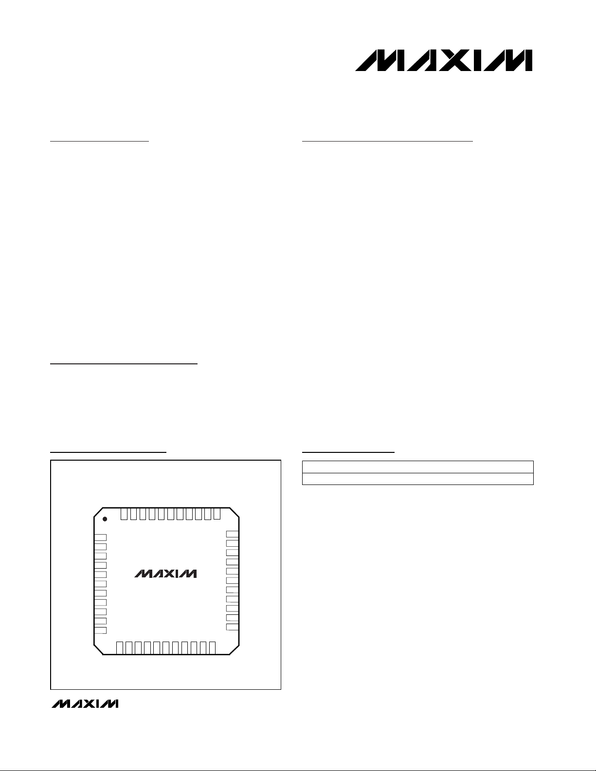
Ordering InformationPin Configuration
44 QFN-EP*
PIN-PACKAGETEMP. RANGE
0°C to +85°CMAX2114UGH
PART
PLLINPLLIN+
MODMOD+
IOUT+
IOUTV
CC
QOUT+
QOUTRFBAND
FLCLK
V
CC
CFLT
XTL-
XTL+
GND
V
CC
RFIN+
RFIN-
GND
QDC-
QDC+
1
2
3
4
5
6
7
8
9
10
11
1213141516171819202122
4443424140393837363534
33
32
31
30
29
28
27
26
25
24
23
IDC-
IDC+
LOBUFSEL
RFOUT
CPG1
V
CC
XTLOUT
CPG2
GC1
GC2
INSEL
CPFBGND
V
CC
TANK+
VRLO
TANK-
LODIVSEL
VCCLOBUF-/PSOUT-
LOBUF+/PSOUT+
QFN-EP
MAX2114
TOP VIEW
U.S. DSS Set-Top Receivers
European DVB-Compliant
Systems
Cellular Base Stations
Wireless Local Loop
Broadband Systems
LMDS
Professional Receivers
VSAT
Microwave Links
For price, delivery, and to place orders, please contact Maxim Distribution at 1-888-629-4642,
or visit Maxim’s website at www.maxim-ic.com.
*Exposed paddle
Page 2
MAX2114
DBS Direct Downconverter
2 _______________________________________________________________________________________
ABSOLUTE MAXIMUM RATINGS
DC ELECTRICAL CHARACTERISTICS
(VCC= +4.75V to +5.25V, VFB= +2.4V, C
IOUT_
= C
QOUT_
= 10pF, f
FLCLK
= 2MHz, RFIN_ = unconnected, R
IOUT_
= R
QOUT_
= 10kΩ,
V
LOBUFSEL
= +0.5V, V
R
FBAND
= V
INSEL
= V
CPG1
= V
CPG2
= +2.4V, V
PLLIN+
= V
MOD+
= +1.3V, V
PLLIN-
= V
MOD-
= +1.1V, TA=
+25°C, unless otherwise noted. Typical values are at V
CC
= +5V, unless otherwise noted.)
Stresses beyond those listed under “Absolute Maximum Ratings” may cause permanent damage to the device. These are stress ratings only, and functional
operation of the device at these or any other conditions beyond those indicated in the operational sections of the specifications is not implied. Exposure to
absolute maximum rating conditions for extended periods may affect device reliability.
VCCto GND..............................................................-0.3V to +7V
All Other Pins to GND................................-0.3V to (V
CC
+ 0.3V)
RFIN+ to RFIN-, TANK+ to TANK-,
IDC+ to IDC-, QDC+ to QDC- .........................................±2V
IOUT_, QOUT_ to GND Short-Circuit Duration .......................10s
LOBUF+/PSOUT+, LOBUF-/PSOUT- Short-Circuit Duration..10s
VRLO Short-Circuit Duration.....................................................0s
Continuous Current (any pin other than V
CC
or GND)........20mA
Continuous Power Dissipation (T
A
= +70°C)
44-Pin QFN-EP (derate 27mW/°C above +70°C)............1.8W
Operating Temperature ..........................................0°C to +85°C
Junction Temperature......................................................+150°C
Storage Temperature Range .............................-65°C to +150°C
Lead Temperature (soldering, 10s) .................................+300°C
XTLOUT Output DC Voltage 1.9 V
RFBAND Input Current -200 200 µA
1.44 1.8 2.16
mA
0.48 0.6 0.72
V
CPG1
≥ 2.4V, V
CPG2
≥ 2.4V
V
CPG1
≥ 2.4V, V
CPG2
≤ 0.5V
0.24 0.3 0.36V
CPG1
≤ 0.5V, V
CPG2
≥ 2.4V
Operating Supply Current I
CC
195 275
mA
PARAMETER SYMBOL MIN TYP MAX UNITS
Input Current I
IN
-15 10 µA
Input Voltage Low V
IL
0.5 V
Input Voltage High V
IH
2.4 V
FLCLK Input Voltage High 1.85 V
FLCLK Input Voltage Low 1.45 V
FLCLK Input Current (Note 1) -1 1 µA
Operating Supply Voltage V
CC
4.75 5.25 V
Common-Mode Input Voltage V
CMI
1.08 1.2 1.32 V
Input Voltage Low -100 mV
Input Voltage High 100 mV
Input Current (Note 1)
-5 5
µA
Common-Mode Output Voltage V
CMO
2.16 2.4 2.64 V
Output Voltage Low (Note 2) -150 mV
Output Voltage High (Note 2) 150 mV
Prescaler Ratio
Reference Divider Ratio 88
Charge-Pump Output High
Measured at FB
0.08 0.1 0.12
CONDITIONS
Referenced to V
CMI
Referenced to V
CMI
R
SOURCE
= 50kΩ, V
FLCLK
= 1.65V
Referenced to V
CMO
, LOBUFSEL ≤ 0.5V
Referenced to V
CMO
, LOBUFSEL ≤ 0.5V
V
CPG1
≤ 0.5V, V
CPG2
≤ 0.5V
(V
MOD+-VMOD-
) ≥ 200mV, LOBUFSEL ≤ 0.5V 32 32
LOBUFSEL ≥ 2.4V, LODIVSEL ≤ 0.5V
LOBUFSEL ≥ 2.4V, LODIVSEL ≥ 2.4V
(V
MOD+-VMOD-
) ≤ -200mV, LOBUFSEL ≤ 0.5V
22
11
33 33
FREQUENCY SYNTHESIZER/LO BUFFER
DIFFERENTIAL DIGITAL OUTPUTS (LOBUF+/PSOUT+, LOBUF-/PSOUT-)
DIFFERENTIAL DIGITAL INPUTS (MOD+, MOD-, PLLIN+, PLLIN-)
SLEW-RATE-LIMITED DIGITAL INPUT (f
FLCLK
)
STANDARD DIGITAL INPUTS (INSEL, CPG1, CPG2, LOBUFSEL, LODIVSEL, RFBAND)
Page 3
MAX2114
DBS Direct Downconverter
_______________________________________________________________________________________ 3
DC ELECTRICAL CHARACTERISTICS (continued)
(VCC= +4.75V to +5.25V, VFB= +2.4V, C
IOUT_
= C
QOUT_
= 10pF, f
FLCLK
= 2MHz, RFIN_ = unconnected, R
IOUT_
= R
QOUT_
= 10kΩ,
V
LOBUFSEL
= +0.5V, V
R
FBAND
= V
INSEL
= V
CPG1
= V
CPG2
= +2.4V, V
PLLIN+
= V
MOD+
= +1.3V, V
PLLIN-
= V
MOD-
= +1.1V, TA=
+25°C, unless otherwise noted. Typical values are at V
CC
= +5V, unless otherwise noted.)
AC ELECTRICAL CHARACTERISTICS
(IC driven single-ended with RFIN- AC-terminated in 75Ω to GND, V
CC
= +4.75V to +5.25V, V
IOUT_
= V
QOUT_
= 0.59Vp-p,
C
IOUT_
= C
QOUT_
= 10pF, f
FCLK
= 500kHz, R
IOUT_
= R
QOUT_
= 10kΩ, V
LOBUFSEL
= 0.5V, V
RFBAND
= V
INSEL
= V
CPG1
= V
CPG2
= +2.4V,
V
PLLIN+
= V
MOD+
= +1.3V, V
PLLIN-
= V
MOD-
= +1.1V, TA= +25°C, unless otherwise noted. Typical values are at VCC= +5V.)
V
CPG1
≤ 0.5V, V
CPG2
≤ 0.5V
V
CPG1
≤ 0.5V, V
CPG2
≥ 2.4V
CONDITIONS
-0.12 -0.1 -0.08
Charge-Pump Output Low
Measured at FB
-0.36 -0.3 -0.24
UNITSMIN TYP MAXSYMBOLPARAMETER
V
CPG1
≥ 2.4V, V
CPG2
≤ 0.5V
V
CPG1
≥ 2.4V, V
CPG2
≥ 2.4V
-0.72 -0.6 -0.48
mA
-2.16 -1.8 -1.44
V
GC_
= 1V to 4V -50 50I
GC_
Input Current µA
Charge-Pump Output Current
Matching Positive to Negative
%Measured at FB -5 5
Charge-Pump Output Leakage nAMeasured at FB -25 25
Offset Voltage (Note 1) mV
Differential Output Voltage
Swing
Vp-pRL= 2kΩ differential 1
Common-Mode Output Voltage
(Note 1)
V0.65 0.85
-50 50
Charge-Pump Output Current
Drive (Note 1)
µAMeasured at CP 100
ANALOG CONTROL INPUTS (GC1, GC2)
BASEBAND OUTPUTS (IOUT+, IOUT-, QOUT+, QOUT-)
P
RFIN_
= -25dBm 44.8
P
RFIN_
= -65dBm
fLO= 950MHz
fLO= 1550MHz
fLO= 2175MHz
-26
-29
-30
P
RFIN_
= -65dBm
per tone
fLO= 950MHz
fLO= 1550MHz
fLO= 2175MHz
V
GC1
= V
GC2
= +1V (max gain)
V
GC1
= V
GC2
= +4V (min gain)
2
P
RFIN_
= -40dBm,
signals within filter bandwidth
dBV
Output-Referred 1dB Compression
Point (Note 5)
P1
dBOUT
16.1
P
RFIN_
= -25dBm per tone,
f
LO
= 951MHz
dBm
RFIN_ Input Second-Order Intercept
(Note 4)
IP2
RFIN_
10.7
8.0
11.1
P
RFIN_
= -25dBm
per tone
dBm
RFIN_ Input Third-Order Intercept
Point (Note 3)
IP3
RFIN_
-68
Single
carrier
-25
dBm
RFIN_ Input Power for 0.59Vp-p
Baseband Levels
925 2175
Inferred by quadrature gain and
phase-error test
PARAMETER SYMBOL MIN TYP MAX UNITS
10.6
f
RFIN
_
= 1550MHz,
V
GC1
= 1V, V
GC2
adjusted 0.59Vp-p
baseband level
dBNoise Figure NF
CONDITIONS
MHzRFIN_ Input Frequency Range f
RFIN_
Page 4

MAX2114
DBS Direct Downconverter
4 _______________________________________________________________________________________
AC ELECTRICAL CHARACTERISTICS (continued)
(R
FIN
+ IC driven single-ended with RFIN- AC-terminated in 75Ω to GND, V
CC
= +4.75V to +5.25V, V
IOUT_
= V
QOUT_
= 0.59Vp-p,
C
IOUT_
= C
QOUT_
= 10pF, f
FCLK
= 500kHz, R
IOUT_
= R
QOUT_
= 10kΩ, V
LOBUFSEL
= 0.5V, V
RFBAND
= V
INSEL
= V
CPG1
= V
CPG2
= +2.4V,
V
PLLIN+
= V
MOD+
= +1.3V, V
PLLIN-
= V
MOD-
= +1.1V, TA= +25°C, unless otherwise noted. Typical values are at VCC= +5V.)
RFOUT PORT (LOOPTHROUGH)
dBm
LO Leakage Power (Notes 6, 9) Measured at R
FIN
+ -66
dBLO Half Harmonic Rejection (Note 8) Average level of V
IOUT_
, VQOUT_
Average level of V
IOUT_
, V
QOUT_
dB45LO 2nd Harmonic Rejection (Note 7)
43
f
RFIN_
= 925MHz, Z
SOURCE
= 75Ω +13
CONDITIONS UNITSMIN TYP MAXSYMBOLPARAMETER
f = 1550MHz
f = 2175MHz
f = 1550MHz 10.6
f = 2175MHz 10.8
RFOUT Return Loss (Notes 6, 10) dB925MHz < f < 2175MHz, Z
LOAD
= 75Ω 12
LPF -3dB Cutoff-Frequency Range
(Note 1)
MHzControlled by FLCLK signal 833
-5.5 5.5
-10 10
LPF -3dB Cutoff-Frequency
Accuracy (Note 1)
%
10 10
dBR
FIN
+ Return Loss (Note 6)
Ratio of In-Filter-Band to Out-of-FilterBand Noise
dB
1.2
f
IN_BAND
= 100Hz to 22.5MHz,
f
OUT_BAND
= 67.5MHz to 112.5MHz
23
Baseband Highpass -3dB Frequency
(Note 1)
HzC
IDC_
= C
QDC_
= 0.22µF 750
Baseband Frequency Response
(Note 1)
dB
Deviation from ideal 7th order,
Butterworth, up to 0.7 × f
C
-0.5 0.5
f
FLCLK
= 0.5MHz, fC = 8MHz
f
FLCLK
= 1.25MHz, fC = 19.3MHz
f
FLCLK
= 2.0625MHz, fC = 31.4MHz
Includes effects from baseband filters,
measured at 125kHz baseband
Quadrature Gain Error dB
4
Includes effects from baseband filters,
measured at 125kHz baseband
Quadrature Phase Error degrees
RFIN+ to RFOUT Gain (Note 10) dB
f = 925MHz 0.5
f = 2175MHz 2.0
f = 1550MHz 1.0
RFOUT Output Third-Order Intercept
Point (Note 10)
dBm
f = 925MHz 9.5
7.7
5.4
RFOUT Noise Figure (Note 10) dB
f = 925MHz 12
f
RFIN_
= 2175MHz, Z
SOURCE
= 75Ω +14
RFOUT PORT (LOOPTHROUGH)
Output Real Impedance (Notes 1) ΩIOUT_, QOUT_ 50
Page 5

MAX2114
DBS Direct Downconverter
_______________________________________________________________________________________ 5
Note 1: Minimum and maximum values are guaranteed by design and characterization over supply voltage.
Note 2 Driving differential load of 10kΩ || 15pF.
Note 3: Two signals are applied to RFIN_ at (f
LO
- 100MHz) and (fLO- 199MHz). V
GC2
= 1V, V
GC1
is set so that the baseband out-
puts are at 590mVp-p. IM products are measured at baseband outputs but are referred to RF inputs.
Note 4: Two signals are applied to RFIN_ at 1200MHz and 2150MHz. V
GC2
= 1V, V
GC1
is set so that the baseband outputs are at
590mVp-p. IM products are measured at baseband outputs but are referred to RF inputs.
Note 5: P
RFIN_
= -40dBm so that front-end IM contributions are minimized.
Note 6: Using L64733/L64734 demo board from LSI Logic.
Note 7: Downconverted level, in dBc, of carrier present at f
LO
× 2, fLO= 1180MHz, f
VCO
= 590MHz, V
RFBAND
= unconnected.
Note 8: Downconverted level, in dBc, of carrier present at f
O
/ 2, fLO= 2175MHz, f
VCO
= 1087.5MHz, V
RFBAND
= 2.4V.
Note 9: Leakage is dominated by board parasitics.
Note 10: V
CPG1
= V
CPG2
= V
RFBAND
= V
INSEL
= 0.5V, f
FLCLK
= 0.5MHz.
Note 11: Guaranteed by design and characterization over supply and temperature.
Note 12: Measured at tuned frequency with PLL locked. PLL loop bandwidth = 3kHz. All phase noise measurements assume tank
components have a Q > 50.
AC ELECTRICAL CHARACTERISTICS (continued)
(IC driven single-ended with RFIN- AC-terminated in 75Ω to GND, V
CC
= +4.75V to +5.25V, V
IOUT_
= V
QOUT_
= 0.59Vp-p,
C
IOUT_
= C
QOUT_
= 10pF, f
FCLK
= 500kHz, R
IOUT_
= R
QOUT_
= 10kΩ, V
LOBUFSEL
= 0.5V, V
RFBAND
= V
INSEL
= V
CPG1
= V
CPG2
= +2.4V,
V
PLLIN+
= V
MOD+
= +1.3V, V
PLLIN-
= V
MOD-
= +1.1V, TA= +25°C, unless otherwise noted. Typical values are at VCC= +5V.)
LOCAL OSCILLATOR
SYNTHESIZER
-96
PARAMETER SYMBOL MIN TYP MAX UNITS
At 100kHz offset, fLO= 2175MHz
dBc/HzLO Phase Noise (Notes 6, 12)
-75At 10kHz offset, fLO= 2175MHz
58
0Figure 1
f
RFIN
= 2175MHz dBRFIN+ to LO Input Isolation (Note 9)
-60
590 1180 MHzLO Tuning Range (Note 11)
ns
4 7.26 MHzCrystal Frequency Range (Note 1)
0.8 1 1.5Load = 10pF ||10kΩ, f
XTLOUT
= 4MHz Vp-pXTLOUT Output Voltage Swing
At 1kHz offset, fLO= 2175MHz
MOD+, MOD- Hold Time (Note 1) t
HM
7Figure 1
CONDITIONS
nsMOD+, MOD- Setup Time (Note 1) t
SUM
70
V
LOBUFSEL
≥ 2.4V,
fLO= 925 MHz + 2175MHz
mV
RMS
LO Buffer Output Voltage (Note 1)
SYNTHESIZER
LOCAL OSCILLATOR
Page 6

MAX2114
DBS Direct Downconverter
6 _______________________________________________________________________________________
Pin Description
PECL Modulus Control. A PECL high on MOD+ sets the dual-modulus prescaler to divide by 32. A PECL
logic low sets the divide ratio to 33. Drive with a differential PECL signal in conjunction with MOD- (pin 31).
MOD+30
Local Oscillator Buffer Select. Connect to GND to select DIV32/33 prescaler output; connect VCCto
DIV1 to select DIV2 LO buffer output.
LOBUFSEL14
VCCPower-Supply Input. Connect each pin to a +5V ±5% low-noise supply. Bypass each VCCpin to
the nearest GND with a ceramic chip capacitor.
V
CC
1, 6, 17,
27, 36, 41
Baseband In-Phase Output. Connect to noninverting input of high-speed ADC.IOUT+29
Baseband In-Phase Output. Connect to inverting input of high-speed ADC.IOUT-28
Baseband Quadrature Output. Connect to noninverting input of high-speed ADC.QOUT+26
Baseband Quadrature Output. Connect to inverting input of high-speed ADC.QOUT-25
RF Input Band Select Input. Drive high to enable 1680MHz to 2175MHz band. Leave unconnected to
enable 1180MHz to 1680MHz band. Connect to GND to enable 925MHz to 1180MHz band.
RFBAND24
Baseband Filter Cutoff Adjust. Connect to a slew-rate-limited clock source. See AC Electrical
Characteristics for transfer function.
FLCLK23
Loopthrough Mode Enable. High-impedance digital input. Drive low to enable the RFOUT buffer and
disable the LO converters. Drive high for normal tuner operation.
INSEL22
Gain Control Input for Baseband Signals. High-impedance analog input, with an input range of +1V to
+4V. See AC Electrical Characteristics for transfer function.
GC221
Gain Control Input for RF Front End. High-impedance analog input, with an input range of +1V to +4V.
See AC Electrical Characteristics for transfer function.
GC120
Charge-Pump Gain Select. High-impedance digital input. Sets the charge-pump output scaling. See
DC Electrical Characteristics for available gain settings.
CPG219
Buffered Crystal Oscillator OutputXTLOUT18
Charge-Pump Gain Select. High-impedance digital input. Sets the charge-pump output scaling. See
DC Electrical Characteristics for available gain settings.
CPG116
Buffered RF Output. Enabled when INSEL is low.RFOUT15
Baseband Offset Correction. Connect a 0.22µF ceramic chip capacitor from IDC+ to IDC- (pin 12).IDC+13
Baseband Offset Correction. Connect a 0.22µF ceramic chip capacitor from IDC- to IDC+ (pin 13).IDC-12
Baseband Offset Correction. Connect a 0.22µF ceramic chip capacitor from QDC+ to QDC- (pin 10).QDC+11
Baseband Offset Correction. Connect a 0.22µF ceramic chip capacitor from QDC- to QDC+ (pin 11).QDC-10
RF Noninverting Input. Connect to 75Ω source with a 47pF ceramic chip capacitor.RFIN+8
RF Inverting Input. Bypass RFIN- with 47pF capacitor in series with a 75Ω resistor to GND.RFIN-7
Ground. Connect each of these pins to a solid ground plane. Use multiple vias to reduce inductance
where possible.
GND5, 9, 42
Noninverting Input to Crystal Oscillator. Consult crystal manufacturer for circuit loading requirements.XTL+4
Inverting Input to Crystal Oscillator. Consult crystal manufacturer for circuit loading requirements.XTL-3
External Bypass for Internal Bias. Bypass this pin with a 0.22µF ceramic chip capacitor to GND.
CFLT2
PIN FUNCTIONNAME
Page 7

MAX2114
DBS Direct Downconverter
_______________________________________________________________________________________ 7
Pin Description (continued)
Figure 1. Modulus Control Timing Diagram
Voltage Drive Output. Control of external charge-pump transistor.CP44
Feedback Input for Loop FilterFB43
LO Tank Oscillator Input. Connect to an external LC tank with varactor tuning.TANK+40
LO Internal Regulator. Bypass with a 1000pF ceramic chip capacitor to GND.VRLO39
LOBUFSEL = GND: PECL Prescaler Output. Differential output of the dual-modulus prescaler. Used in
conjunction with PSOUT+. Requires PECL-compatible termination. LOBUFSEL = VCC: 50Ω LO buffer
inverting output.
LOBUF-/
PSOUT-
35
LO Tank Oscillator Input. Connect to an external LC tank with varactor tuning.TANK-38
PECL Phase-Locked Loop Input. Drive with a differential PECL signal in conjunction with PLLIN+ (pin 32).PLLIN-33
LOBUFSEL = GND: PECL Prescaler Output. Differential output of the dual-modulus prescaler. Used in
conjunction with PSOUT-. Requires PECL-compatible termination. LOBUFSEL = V
CC
: 50Ω LO buffer
noninverting output.
LOBUF+/
PSOUT+
34
PECL Phase-Locked Loop Input. Drive with a differential PECL signal in conjunction with PLLIN- (pin 33).PLLIN+32
PECL Modulus Control. A PECL low on MOD- sets the dual-modulus prescaler to divide by 32. A
PECL logic high sets the divide ratio to 33. Drive with a differential PECL signal in conjunction with
MOD+ (pin 30).
MOD-31
PIN FUNCTIONNAME
LO Buffer Divider Ratio Input. Drive high to enable divide-by-one LO buffer output. Connect to GND to
enable divide-by-two buffer output.
LODIVSEL37
MOD+,
MOD-
PSOUT+
PSOUT-
50%
t
SUM
t
HM
50%
50%
50%
Page 8

MAX2114
DBS Direct Downconverter
Functional Diagram
Package Information
For the latest package outline information, go to
www.maxim-ic.com/packages.
Maxim cannot assume responsibility for use of any circuitry other than circuitry entirely embodied in a Maxim product. No circuit patent licenses are
implied. Maxim reserves the right to change the circuitry and specifications without notice at any time.
8 _____________________Maxim Integrated Products, 120 San Gabriel Drive, Sunnyvale, CA 94086 408-737-7600
© 2001 Maxim Integrated Products Printed USA is a registered trademark of Maxim Integrated Products.
CPG1
CPG2
PLLIN+
PLLIN-
XTL+
XTL-
LODIVSEL
MOD+
MOD-
RFBAND
TANK+
TANK-
V
VRLO
CFLT
GND
RFIN+
RFIN-
GC1
GC2
FLCLK
INSEL
MAX2114
CHARGE
PUMP
/8
/132,33
1, 2
x2
CC
VOLTAGE
REGULATOR
90°
BASEBAND
OFFSET
CORRECTION
CP
FB
XTLOUT
LOBUFSEL
LOBUF+/PSOUT+
LOBUF-/PSOUT-
IDC+
IDCQDC+
QDC-
IOUT+
IOUT-
QOUT+
QOUT-
RFOUT
 Loading...