

Page 1

For free samples & the latest literature: http://www.maxim-ic.com, or phone 1-800-998-8800.
For small orders, phone 1-800-835-8769.
General Description
The MAX2108 is a low-cost direct-conversion tuner IC
designed for use in digital direct-broadcast satellite
(DBS) television set-top box units and microwave links.
Its direct-conversion architecture reduces system cost
compared to devices with IF-based architectures.
The MAX2108 directly tunes L-band signals to baseband using a broadband I/Q downconverter. The operating frequency range spans from 950MHz to
2150MHz. The IC includes a low-noise amplifier (LNA)
with gain control, two downconverter mixers with output
buffers, a 90° quadrature generator, and a divide-by
32/33 prescaler.
Applications
DirecTV, PrimeStar, EchoStar DBS Tuners
DVB-Compliant DBS Tuners
Cellular Base Stations
Wireless Local Loop
Broadband Systems
LMDS
Microwave Links
Features
♦ Low-Cost Architecture
♦ Operates from Single +5V Supply
♦ On-Chip Quadrature Generator, Dual-Modulus
Prescaler (/32, /33)
♦ Input Levels: -20dBm to -70dBm per Carrier
♦ Over 50dB RF Gain-Control Range
♦ 10dB Noise Figure at Maximum Gain
♦ +8dBm IIP3 at Minimum Gain
MAX2108
Direct-Conversion Tuner IC
________________________________________________________________
Maxim Integrated Products
1
PS_SEL GC GND GND RFIN
RFIN
GND IOUT
IOUT
PSOUT
V
CC
V
CC
V
CC
V
CC
PSOUT GND GND N.C. LO LO QOUT QOUT
N.C. GND
1211109 876543 21
13 14 15 16 17 18 19 20 21 22 23 24
MAX2108
/32
/33
90
Q
0
I
Functional Diagram
19-1449; Rev 0; 4/99
PART
MAX2108CEG 0°C to +70°C
TEMP. RANGE PIN-PACKAGE
24 QSOP
Ordering Information
Pin Configuration appears at end of data sheet.
Page 2

MAX2108
Direct-Conversion Tuner IC
2 _______________________________________________________________________________________
ABSOLUTE MAXIMUM RATINGS
DC ELECTRICAL CHARACTERISTICS
(VCC= +4.75V to +5.25V; VGC= 1.3V; PS_SEL = 0.5V; IOUT, IOUT, QOUT, QOUT = terminated with 2.5kΩ to GND; no input signal
applied; T
A
= 0°C to +70°C; unless otherwise noted. Typical values are at VCC= +5V, TA= +25°C.)
AC ELECTRICAL CHARACTERISTICS
(VCC= +5V; PS_SEL = 0.5V; P
RFIN
= -20dBm; fLO= f
RFIN
+125kHz; GC set via servo loop for V
IOUT
- V
IOUT
= 200mVp-p (differen-
tial); T
A
= +25°C; unless otherwise noted.)
Stresses beyond those listed under “Absolute Maximum Ratings” may cause permanent damage to the device. These are stress ratings only, and functional
operation of the device at these or any other conditions beyond those indicated in the operational sections of the specifications is not implied. Exposure to
absolute maximum rating conditions for extended periods may affect device reliability.
VCCto GND..............................................................-0.3V to +7V
V
CC
to Any Other VCC...........................................-0.3V to +0.3V
All Other Pins to GND.................................-0.3V to (V
CC
+ 0.3V)
RFIN to RFIN ..........................................................................±2V
LO to LO ................................................................................±2V
Short-Circuit Current
IOUT, IOUT, QOUT, QOUT to GND.................................10mA
PSOUT, PSOUT to GND...................................................40mA
Short-Circuit Duration IOUT to IOUT, QOUT to QOUT,
PSOUT to PSOUT ............................................................10sec
Continuous Power Dissipation (T
A
= +70°C)
24 QSOP (derate 10mW/°C above T
A
= +70°C) ..........800mW
Operating Temperature Range...............................0°C to +70°C
Junction Temperature......................................................+150°C
Storage Temperature Range.............................-65°C to +150°C
Lead Temperature (soldering, 10sec).............................+300°C
0 < V
PS_SEL
< V
CC
1V < VGC< 4V
CONDITIONS
V0.5V
THL
PS_SEL Logic-Low Threshold
V2.4V
THH
mA105 152I
CC
Supply Current
PS_SEL Logic-High Threshold
µA-30 +10I
PS_SEL
PS_SEL Input Bias Current
µA-80 +80I
GC
GC Input Bias Current
UNITSMIN TYP MAXSYMBOLPARAMETER
V2.9 3.35 3.8V
CM
IOUT, IOUT, QOUT, QOUT
Common-Mode Output Voltage
950MHz < f
RFIN
< 2150MHz, PLO= -5dBm,
V
IOUT
- V
IOUT
= 10mVp-p, TA= 0°C +70°C
950MHz < f
RFIN
< 2150MHz, PLO= -5dBm
1V < VGC< 4V, PLO= -5dBm
CONDITIONS
dBm-70P
RFINMIN
RFIN Minimum Input Power
(Note 2)
dBm-20P
RFINMAX
MHz950 2150f
RFIN
RFIN Frequency Range (Note 1)
RFIN Maximum Input Power
(Note 2)
dBm
-5
External LO Drive Level (Note 2)
dB50Gain-Control Range (Note 2)
UNITSMIN TYP MAXSYMBOLPARAMETER
VGC= 4V, fLO= 1750MHz dB10NFNoise Figure
dBm14IIP
2
dBm8IIP
3
RFIN Input Third-Order
Intercept Point (Note 3)
RFIN Input Second-Order
Intercept Point (Note 4)
Page 3

MAX2108
Direct-Conversion Tuner IC
_______________________________________________________________________________________ 3
AC ELECTRICAL CHARACTERISTICS (continued)
(VCC= +5V; PS_SEL = 0.5V; P
RFIN
= -20dBm; fLO= f
RFIN
+125kHz; GC set via servo loop for V
IOUT
- V
IOUT
= 200mVp-p (differen-
tial); T
A
= +25°C; unless otherwise noted.)
Note 1: AC specifications with minimum/maximum limits are met within this frequency range.
Note 2: LO and LO are differentially driven through an AC-coupled matching network.
Note 3: P
RFIN
= -20dBm per tone, GC set via servo loop for V
IOUT
- V
IOUT
= 20mVp-p per tone. f1
RFIN
= 1749MHz, f2
RFIN
=
1751MHz, f
LO
= 1740MHz.
Note 4: P
RFIN
= -20dBm per tone, GC set via servo loop for V
IOUT
- V
IOUT
= 20mVp-p per tone. f1
RFIN
= 1200MHz, f2
RFIN
=
2150MHz, f
LO
= 951MHz.
CONDITIONS UNITSMIN TYP MAXSYMBOLPARAMETER
V
PS_SEL
< 0.5V
C
PSOUT
= C
PSOUT
= 10pF to GND
33 33
V
PS_SEL
> 2.4V
Prescaler Divide Ratio
Vp-p1.0
V
PSOUT -
V
PSOUT
Differential Prescaler Output
Swing
32 32
At -3dB attenuation
f
IOUT
= f
IOUT
= f
QOUT
= f
QOUT
= 20MHz
MHz150
f
IOUT
= f
IOUT
= f
QOUT
= f
QOUT
= 125kHz
Baseband Bandwidth
Ω33
I/Q Channel Differential
Output Impedance
degrees3
I/Q Channel Quadrature
Phase Error (Note 2)
f
IOUT
= f
IOUT
= f
QOUT=fQOUT
= 125kHz dB1
I/Q Amplitude Mismatch
(Note 2)
f
IOUT
= f
IOUT
= f
QOUT
= f
QOUT
= 10MHz,
no output load
Vp-p1.4I/Q Channel Clipping Level
Typical Operating Characteristics
(TA = +25°C, unless otherwise noted.)
90
100
95
110
105
120
115
125
4.75 4.954.85 5.05 5.15 5.25
SUPPLY CURRENT
vs. SUPPLY VOLTAGE
MAX2108 toc01
VCC(V)
I
CC
(mA)
TA = +70°C
TA = +25°C
TA = 0°C
-80
-70
-60
-50
-40
-30
-20
-10
0
1 1.5 2 2.5 3 3.5
CARRIER LEVEL vs. GAIN CONTROL
MAX2108 toc02
GC VOLTAGE (V)
RF LEVEL (dBm)
GC SET FOR 10mVp-p
BASEBAND OUTPUT
f
RFIN
= 1750 MHz
0
2
4
6
8
10
900 13001100 1500 1700
INPUT IP3 vs. FREQUENCY
MAX2108 toc03
RF FREQUENCY (MHz)
IIP3 (dBm)
TWO-TONE FREQUENCY
SPACING EQUALS 2MHz
Page 4

MAX2108
Direct-Conversion Tuner IC
4 _______________________________________________________________________________________
Typical Operating Characteristics
(TA = +25°C, unless otherwise noted.)
0
20
10
30
60
70
50
40
80
-55 -45 -40 -35 -30-50 -25 -20 -15 -10
IM3 vs. CARRIER LEVEL
MAX2108 toc04
RF INPUT LEVEL (dBm)
IM3 (dBc)
TWO-TONE FREQUENCY
SPACING EQUALS 2MHz
5
7
6
9
8
11
10
12
14
13
15
950 1150 1350 1550 1750
NOISE FIGURE vs. FREQUENCY
MAX2108 toc05
RF FREQUENCY (MHz)
NF (dB)
VGC = 4V
5
10
15
20
25
20 26 2822 24 30 32 34 36 38
NOISE FIGURE vs. INSERTION GAIN
(RF TO BASEBAND)
MAX2108 toc06
GAIN (dB)
NF (dB)
-40
-20
-30
20
10
0
-10
40
30
900 1100 1300 1500 1700 1900 2100
RF PORT SERIES IMPEDANCE
vs. FREQUENCY
MAX2108 toc07
FREQUENCY (MHz)
SERIES IMPEDANCE (Ω)
VGC = 4V
REAL
IMAGINARY
-70
-40
-50
-60
-20
-30
20
10
0
-10
40
30
900 1100 1300 1500 1700 1900 2100
RF PORT SERIES IMPEDANCE
vs. FREQUENCY
MAX2108 toc08
FREQUENCY (MHz)
SERIES IMPEDANCE (Ω)
REAL
IMAGINARY
VGC = 1V
-70
-40
-50
-60
-20
-30
20
10
0
-10
30
900 1100 1300 1500 1700 1900 2100
LO PORT SERIES IMPEDANCE
vs. FREQUENCY
MAX2108 toc10
FREQUENCY (MHz)
SERIES IMPEDANCE (Ω)
REAL
IMAGINARY
SINGLE-ENDED
0.1 101 100 1000
NORMALIZED BASEBAND GAIN
vs. BASEBAND FREQUENCY
MAX2108 toc11
BASEBAND FREQUENCY (MHz)
NORMALIZED BASEBAND GAIN (dB)
5
-5
0
Page 5

MAX2108
Direct-Conversion Tuner IC
_______________________________________________________________________________________ 5
NAME FUNCTION
1
IOUT
Inverting I-Channel Baseband Output
PIN
Pin Description
2 IOUT Noninverting I-Channel Baseband Output
3 V
CC
Downconverter +5V Supply. Bypass with a 10pF capacitor to GND as close to the IC as possible. Connect
an additional 0.1µF capacitor in parallel with the 10pF capacitor.
4 GND Ground. Connect to a low-inductance ground plane.
5 V
CC
RF +5V Supply. Bypass with a 22pF capacitor to GND as close to the IC as possible.
6
RFIN
Inverting RF Input. Connect to a 22pF capacitor in series with a 75Ω resistor to GND.
7 RFIN Noninverting RF Input. Connect via matching network to a 75Ω cable.
8, 9 GND RF Ground. Connect to a low-inductance ground plane.
10 GC
Gain-Control Input. Apply a voltage between 1V and 4V to control the gain of the RF amplifier. Bypass with a
1000pF capacitor to minimize noise on the control line.
11 PS_SEL
Prescaler Modulus Control. Drive PS_SEL <0.5V to operate in divide-by-33 mode. Drive PS_SEL >2.4V to
operate in divide-by-32 mode.
12 V
CC
Prescaler +5V Supply. Bypass with a 1000pF capacitor to GND.
13
PSOUT
Inverting Prescaler Output
14 PSOUT Noninverting Prescaler Output
15 GND Prescaler Ground. Connect to a low-inductance ground plane.
16 GND Local Oscillator Ground. Connect to a low-inductance ground plane.
17, 20 N.C. No Connection. Do not make any connection to this pin.
18
LO
Inverting LO Input
19 LO Noninverting LO Input
21 V
CC
Local Oscillator +5V Supply. Bypass with a 22pF capacitor and a 0.1µF capacitor to pin 16.
22 GND Downconverter Ground. Connect to a low-inductance ground plane.
23 QOUT Noninverting Q-Channel Baseband Output
24
QOUT
Inverting Q-Channel Baseband Output
Page 6

MAX2108
Direct-Conversion Tuner IC
6 _______________________________________________________________________________________
_______________Detailed Description
The MAX2108 downconverts signals in the 950MHz to
2150MHz range directly to baseband in-phase/
quadrature-phase (I/Q) signals. It is designed for digital
DBS tuner applications where a direct downconversion
provides a cost savings over multiple-conversion
approaches. However, the MAX2108 is applicable to
any system requiring a broadband I/Q downconversion.
Internally, the MAX2108 consists of a broadband frontend variable gain stage, a quadrature downconverter,
a 90° quadrature generator, a divide-by 32/33
prescaler, and high-linearity I and Q baseband buffers.
The front-end gain-control range is over 50dB.
Specifically, when the MAX2108 operates in an automatic gain control (AGC) loop, VGCis adjusted by the
loop so that a sine wave at RFIN ranging in power from
-70dBm to -20dBm produces a sine wave across IOUT,
IOUT and QOUT, QOUT at 10mVp-p differential. The
noise figure is at its minimum when GC is at its maximum gain setting.
The quadrature downconverter follows the front-end
variable-gain amplifier. The mixer LO ports are fed with
the two LO signals, which are 90° apart in phase.
These quadrature LO signals are generated internally
using the signal from the LO and LO pins.
The resulting I/Q baseband signals are fed through
separate I-channel and Q-channel baseband buffers.
The outputs are capable of driving lowpass filters with
100Ω characteristic impedance (that is, the equivalent
of an AC-coupled 100Ω load). The baseband -3dB output bandwidth is approximately 150MHz.
Applications Information
Front-End Tuner Circuitry
for DBS Tuners
In a typical application, the signal path ahead of the
tuner includes a discrete low-noise amplifier/buffer and
a PIN-diode attenuator. Since the MAX2108 satisfies
the noise and linearity requirements for DBS, this frontend circuitry is not required.
In some very high linearity applications, such as single
channel-per-carrier (SCPC), a varactor-tuned preselection bandpass filter is added between a discrete
LNA and the MAX2108. The filter provides a means of
broadly filtering adjacent interference signals, thus
improving the intermodulation performance of the tuner.
Additionally, the filter removes RF interference at twice
the LO frequency, which otherwise adds to the cochannel interference. The MAX2108 rejects this carrier
to approximately 25dBc.
LO Port
The MAX2108 accepts either a single-ended or differential LO signal. For single-ended drive, AC-couple the
LO signal into LO with a 47pF capacitor, and bypass
LO to ground with a 47pF capacitor in series with a
25Ω resistor. Drive LO with a 50Ω source at -5dBm.
Prescaler
The prescaler requires a stable logic level at PS_SEL
4ns before the falling edge of PSOUT, PSOUT to assert
the desired modulus. The logic level at PS_SEL must
remain static until 2ns after this falling edge.
Baseband Buffers
The MAX2108 baseband buffers provide at least
10mVp-p differential swing across IOUT, IOUT and
QOUT, QOUT, and are capable of driving an AC-coupled 100Ω differential load. In a typical application,
IOUT, IOUT, QOUT, and QOUT drive a 5th- or 7th-order
lowpass filter for ADC anti-aliasing purposes (see the
Filters in Direct-Conversion Tuners
section ). In general,
additional gain is required, after the filters. This is
accomplished with a pair of video-speed op amps,
such as the MAX4216 dual video op amp, or a simple
transistor circuit. Contact Maxim for more information
about the MAX4216.
Layout Considerations
Observe standard RF layout rules. A ground plane is
essential; when connecting areas of ground plane
between layers, use vias liberally. If a ground plane is
used under the lowpass filters, note that the filter
response may be slightly offset due to parasitic capacitance.
In a direct-conversion receiver, LO leakage to the RF
input connector is a major issue, since filtering of the
LO is impossible (the LO operates at the same frequency as the RF input). Observe the power-supply bypass
capacitor connections in the
Pin Description
table,
notably pins 3, 5, 12, and 21. Traces from these IC pins
to the bypass capacitors must be kept on the top side
of the board and as short as possible.
Page 7
MAX2108
Direct-Conversion Tuner IC
_______________________________________________________________________________________ 7
Power-Supply Sequencing
The MAX2108 has several +5V supply pins. Configure
the supply layout in a star format, with a bypass capacitor that dominates the rise time of the supply at the
center of the star to ensure that all pins see approximately the same voltage during power-up.
Filters in Direct-Conversion Tuners
Typically, a 5th- or 7th-order L-C lowpass filter is used
for anti-aliasing the ADCs following the MAX2108.
Table 1 offers suggested component values for these
lowpass filters. Figures 1 and 2 describe typical filtering
requirements.
Table 1. Suggested Component Values for Discrete Lowpass Filters
0.1dB Chebyshev,
fC= 30MHz
60
0.1dB Chebyshev,
fC= 20MHz
40
FILTER TYPE
ADC
SAMPLING
RATE
(Msps)
50
50
R
S
(Ω)
11
20
C1
(pF)
620
910
L1
(nH)
41
60
C2
(pF)
910
1500
L2
(nH)
50
75
C3
(pF)
1000
1500
L3
(nH)
41
60
C4
(pF)
20
20
R
L
(kΩ)
50 15 680 39 820 33 Short Open 20
0.1dB Chebyshev,
fC= 20MHz
90
50 9 390 28 620 34 680 28 20
0.1dB Chebyshev,
fC= 45MHz
Page 8

MAX2108
Direct-Conversion Tuner IC
8 _______________________________________________________________________________________
RS
C1 C2 C3 C4
RL
ADCS
DSP
MATCHED
FILTERS
RS
L1
L1
BASEBAND LP FILTER
BASEBAND LP FILTER
L2
L2
L3
L3
0.1µF
0.1µF
RS
C1 C2 C3 C4
RL
RS
L1
L1
L2
L2
L3
L3
0.1µF
0.1µF
IOUT IOUT
MAX2108
QOUT QOUT
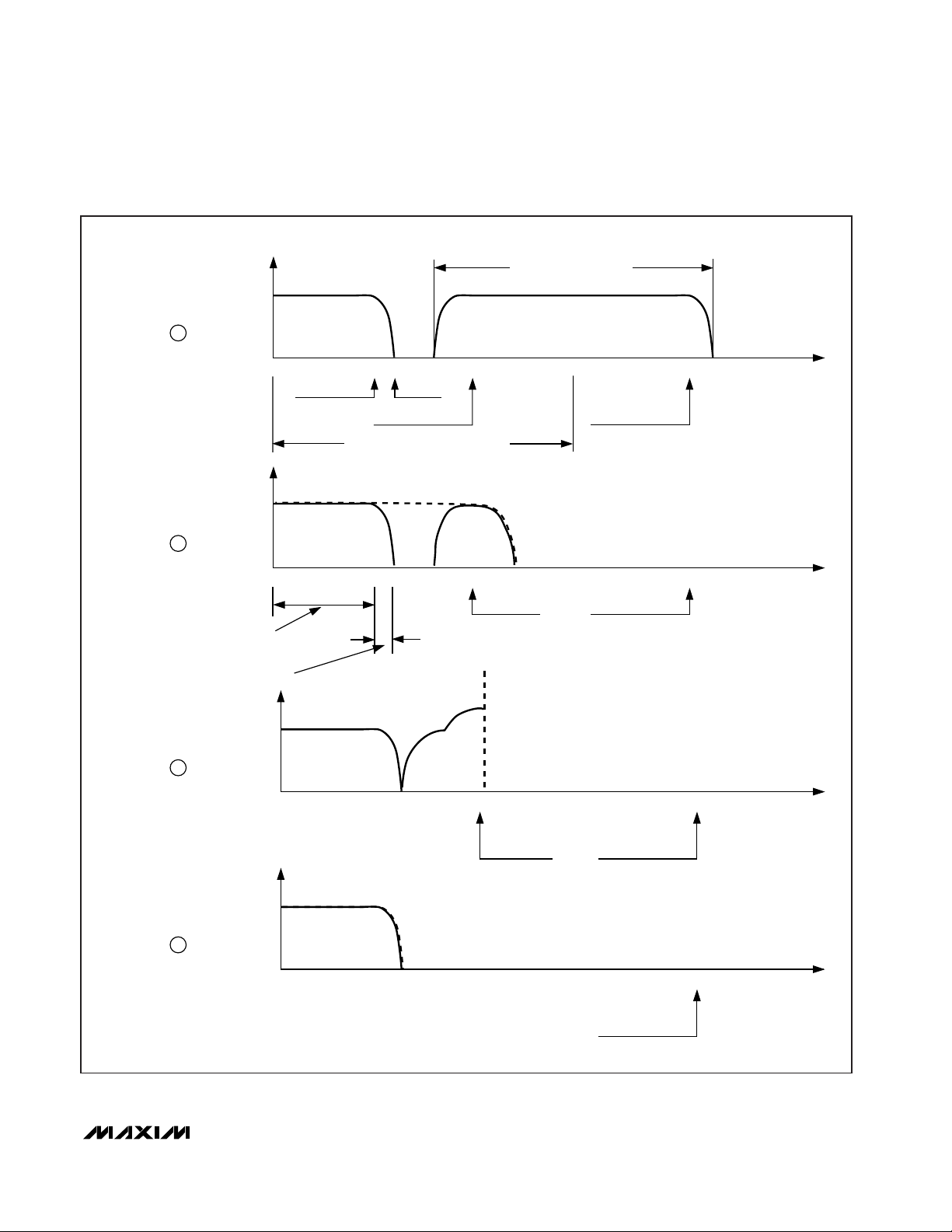
FOR POINTS 1, 2, 3, 4, REFER TO THE SIGNAL SPECTRUMS SHOWN IN FIGURE 2
4
3
2
1
Figure 1. In-Phase and Quadrature-Phase Signal Paths
Page 9
MAX2108
Direct-Conversion Tuner IC
_______________________________________________________________________________________ 9
MHz
DESIRED
CHANNEL
(20Msps)
dBc
AT POINT
0
010
PASSBAND FILTER REQUIREMENTS:
(1) <20% OF BAUD PERIOD DELAY RIPPLE
(2) <0.1dB GAIN RIPPLE
TRANSITION BAND FILTER REQUIREMENTS:
< 2dB GAIN RIPPLE
FILTER CUTOFF
12 20 28 40 MHz17.16
-30
ADC SAMPLING
TRANSPONDER SPACING = 29.16 MHz
LOWPASS FILTER RESPONSE
DESIRED
CHANNEL
(20Msps)
UNDESIRED ADJACENT CHANNEL
TRANSPONDER BW = 24MHz
dBc
AT POINT
0
1
010
DATA NYQUIST
NYQUIST FOR ADC
α = 0.2
12 20 29.16 40 41.1617.16
-30
ADC SAMPLING
MHz
DESIRED
CHANNEL
(20Msps)
ADJ
CHANNEL
FOLDOVER
dBc
AT POINT
0
010
ADC NYQUIST
12 20 4017.16
-30
ADC SAMPLING
MHz
DESIRED
CHANNEL
(20Msps)
FOR POINTS 1, 2, 3, 4, REFER TO FIGURE 1
DIGITAL MATCHED FILTER
dBc
AT POINT
0 10 12 40
-30
ADC SAMPLING
2
3
4
Figure 2. Lowpass Filtering Example
Page 10

MAX2108
Direct-Conversion Tuner IC
10 ______________________________________________________________________________________
24
23
22
21
20
19
18
17
1
2
3
4
5
6
7
8
16
15
14
13
9
10
MODULUS
CONTROL
GAIN
CONTROL
RFIN
11
12
GND
V
CC
IOUT
IOUT
GND
RFIN
RFIN
V
CC
V
CC
PS_SEL
GC
GND
QOUT
QOUT
GND
V
CC
N.C.
LO
LO
N.C.
GND
GND
PSOUT
PSOUT
V
CC
V
CC
V
CC
V
CC
C12
22pF
C13
0.1µF
25Ω
(75Ω SOURCE) R2
75Ω
R1
75Ω
47pF
LO DRIVE
(-5dBm, 50Ω SOURCE)
50Ω
47pF
C4
22pF
C5
22pF
C6
1000pF
C7
1000pF
C3
22pF
C1
10pF
C2
0.1µF
PRESCALER
OUTPUT
MAX2108
BASEBAND
LP
FILTER
BASEBAND
LP
FILTER
Typical Operating Circuit
Page 11
MAX2108
Direct-Conversion Tuner IC
______________________________________________________________________________________ 11
24
23
22
21
20
19
18
17
1
2
3
4
5
6
7
8
QOUT
QOUT
GND
V
CC
GND
V
CC
IOUT
IOUT
TOP VIEW
N.C.
LO
LO
N.C.GND
RFIN
RFIN
V
CC
16
15
14
13
9
10
11
12
GND
GND
PSOUT
PSOUTV
CC
PS_SEL
GC
GND
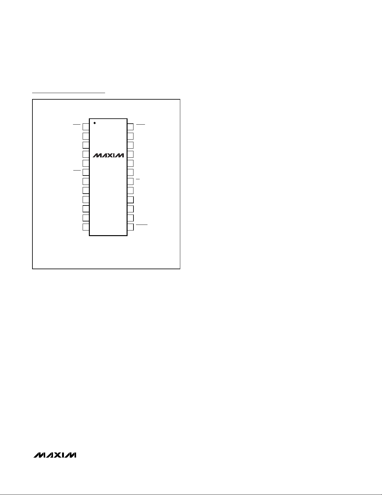
QSOP
MAX2108
Pin Configuration ___________________Chip Information
TRANSISTOR COUNT: 1484
Page 12
MAX2108
Direct-Conversion Tuner IC
Maxim cannot assume responsibility for use of any circuitry other than circuitry entirely embodied in a Maxim product. No circuit patent licenses are
implied. Maxim reserves the right to change the circuitry and specifications without notice at any time.
12
____________________Maxim Integrated Products, 120 San Gabriel Drive, Sunnyvale, CA 94086 408-737-7600
© 1999 Maxim Integrated Products Printed USA is a registered trademark of Maxim Integrated Products.
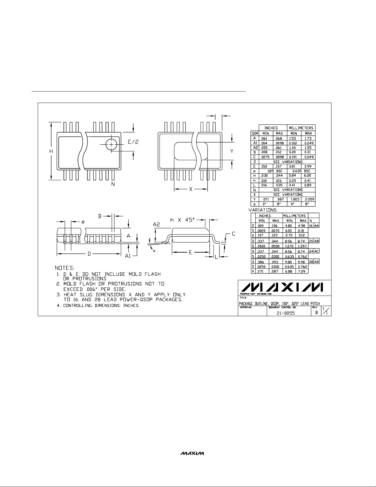
Package Information
QSOP.EPS
 Loading...