

Page 1
General Description
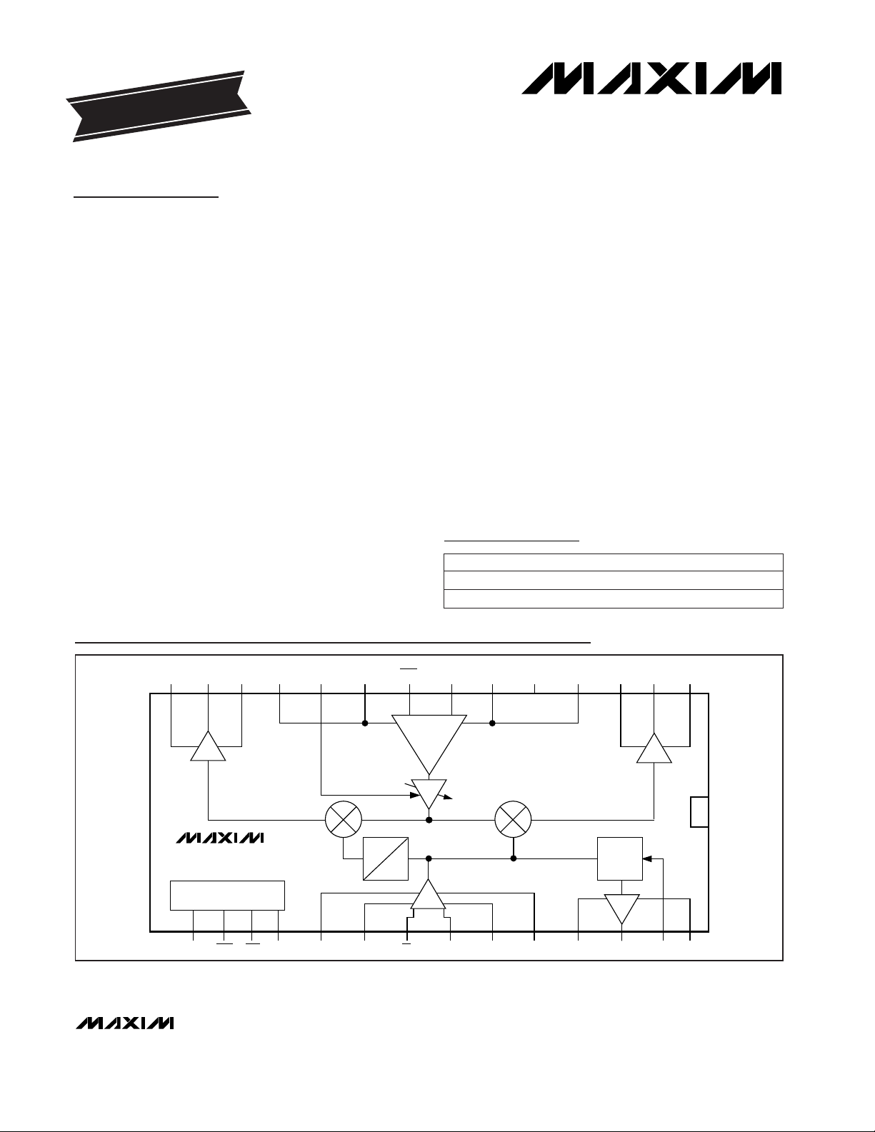
The MAX2102/MAX2105†are low-cost direct-conversion tuner ICs designed for use in digital direct-broadcast satellite (DBS) television set-top box units. The
direct-conversion architecture reduces system cost
compared to devices with IF-based architectures.
The MAX2102/MAX2105 directly tune L-band signals to
baseband using a broadband I/Q downconverter.
Operating frequency range spans from at least 950MHz
to 2150MHz.
The ICs include a low-noise amplifier (LNA) with automatic gain control (AGC), two downconverter mixers,
an oscillator buffer with 90° quadrature generator and
prescaler, and baseband amplifiers.
The MAX2102 features an AGC range of 50dB, allowing
input power levels as low as -69dBm. The MAX2105
has a reduced AGC range of 41dB and accepts input
power levels down to -60dBm. The reduced AGC range
of the MAX2105 allows the use of a high-gain external
LNA to achieve a lower system noise figure (NF).
________________________Applications
DBS Tuners Wireless Local Loop
DVB-Compliant DBS Tuners Broadband Systems
Cellular Base Stations LMDS
____________________________Features
♦ Low-Cost Bipolar Design, Lowest Cost
Architecture
♦ Operate from a Single +5V Supply
♦ 950MHz to 2150MHz Input Frequency Range*
♦ On-Chip Quadrature Generator, Dual-Modulus
Prescaler (/64, /65)
♦ Input Levels
-69dBm to -19dBm per Carrier (MAX2102)
-60dBm to -19dBm per Carrier (MAX2105)
♦ Over 50dB AGC Control Range (MAX2102)
♦ Noise Figure = 13.2dB (MAX2102);
IP3 = 6.5dBm (at 1450MHz)
♦ Automatic Baseband Offset Correction
♦ Easy Interface to MAX1002/MAX1003 Dual ADC
and Popular Baseband ICs
MAX2102/MAX2105
Direct-Conversion Tuner ICs for
Digital DBS Applications
________________________________________________________________
Maxim Integrated Products
1
MAX2102
MAX2105
Q
I
V
CC
QOUT GND GND AGC GND RFIN V
CC
GND V
CC
GND IOUT V
CC
OFFSET CORRECTION
/64, /65
90°
0°
RFIN
QDC
IDC IDC GND V
CC
LO V
CC
GND PSGND PSOUT MOD V
CC
LOQDC
14
1312111098 7654321
15 16 17 18 19 20 21 22
23
24 25 26 27 28
Functional Diagram
19-1256; Rev 2; 10/98
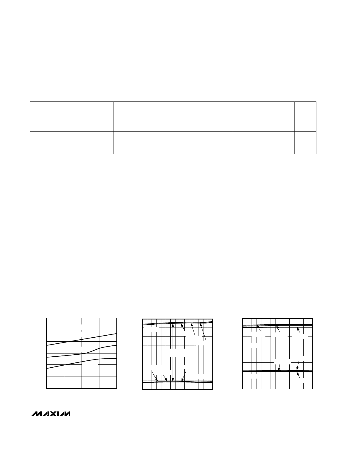
PART
MAX2102CWI
0°C to +70°C
TEMP. RANGE PIN-PACKAGE
28 SO
EVALUATION KIT MANUAL
FOLLOWS DATA SHEET
Ordering Information
†
Patents pending
*
Contact factory for MAX2102/MAX2105 versions with expanded frequency range.
For free samples & the latest literature: http://www.maxim-ic.com, or phone 1-800-998-8800.
For small orders, phone 1-800-835-8769.
MAX2105CWI
0°C to +70°C 28 SO
Page 2
AGC Input Bias Current
MAX2102/MAX2105
Direct-Conversion Tuner ICs for
Digital DBS Applications
2 _______________________________________________________________________________________
ABSOLUTE MAXIMUM RATINGS
DC ELECTRICAL CHARACTERISTICS
(VCC= +4.75V to +5.25V; GND = 0V; PSGND = GND; AGC = 1.3V; MOD = 0.8V; P
RFIN
= OFF, fLO= 1450.125MHz; PLO= -15dBm;
IOUT, QOUT = open; T
A
= 0°C to +70°C; unless otherwise noted.)
AC ELECTRICAL CHARACTERISTICS
(MAX2102 EV kit circuit (Figure 1); VCC= +5V; PSGND = open; MOD = GND; f
RFIN
= 2150MHz; P
RFIN
= -19dBm; fLO=
2150.125MHz; P
LO
= -15dBm driven single-ended into LO; AGC set via servo loop for V
IOUT
= V
QOUT
= 0.5Vp-p; IOUT, QOUT drive
AC-coupled 100Ω loads; 2kΩ from PSOUT to GND; T
A
= +25°C; unless otherwise noted.)
Stresses beyond those listed under “Absolute Maximum Ratings” may cause permanent damage to the device. These are stress ratings only, and functional
operation of the device at these or any other conditions beyond those indicated in the operational sections of the specifications is not implied. Exposure to
absolute maximum rating conditions for extended periods may affect device reliability.
VCCto GND..............................................................-0.5V to +7V
RFIN to
RFIN ..........................................................................±2V
LO to LO ................................................................................±2V
AGC, MOD, RFIN, RFIN, LO, LO to GND.....-0.5V to (V
CC
+ 0.5V)
AGC Current.....................................................................±30mA
IDC to IDC, QDC to QDC.......................................................±2V
IOUT or QOUT to GND Short-Circuit Duration ...................10sec
PSOUT to GND Short-Circuit Duration.................................None
IDC, IDC, QDC, QDC to GND....................-0.5V to (V
CC
+ 0.5V)
Continuous Power Dissipation (T
A
= +70°C)
SO (derate 12.5mW/°C above +70°C)..........................1.025W
Operating Temperature Range...............................0°C to +70°C
Junction Temperature......................................................+150°C
Storage Temperature Range.............................-65°C to +150°C
Lead Temperature (soldering, 10sec).............................+300°C
MAX2102
0V ≤ V
MOD
≤ V
CC
CONDITIONS
mA150 195Quiescent Supply Current
V4.75 5.25Operating Supply Voltage Range
V2.2 2.6IOUT, QOUT Common-Mode Voltage
-250 180
V0.8MOD Input Low Level
V2.0MOD Input High Level
µA-80 10MOD Input Bias Current
UNITSMIN TYP MAXPARAMETER
Refers to single-carrier power generating
V
IOUT
= V
QOUT
= 0.5Vp-p,
950MHz < f
RFIN
< 2150MHz,
950MHz < fLO< 2150MHz (Note 2)
(Note 1)
Refers to single-carrier power generating
V
IOUT
= V
QOUT
= 0.5Vp-p,
950MHz < f
RFIN
< 2150MHz,
950MHz < fLO< 2150MHz (Note 2)
CONDITIONS
dBm
RFIN Maximum Single-Carrier
Input Power
MHz950 2150RFIN Carrier Frequency Range
dBm
-69
RFIN Minimum Single-Carrier
Input Power
50
UNITSMIN TYP MAXPARAMETER
-19
MAX2102
MAX2105 -60
0.5V ≤ V
AGC
≤ 4V
dB
41
AGC Range
MAX2102
MAX2105
RF FRONT END
MAX2105
µA
-180 180
AGC Input Bias Current
SUPPLY
CONTROL INPUTS, PRESCALER
0.5V ≤ V
AGC
≤ 4V
1V ≤ V
AGC
≤ 4V
1V ≤ V
AGC
≤ 4V
Page 3
MAX2102/MAX2105
Direct-Conversion Tuner ICs for
Digital DBS Applications
_______________________________________________________________________________________ 3
AC ELECTRICAL CHARACTERISTICS
(MAX2102 EV kit circuit (Figure 1); VCC= +5V; PSGND = open; MOD = GND; f
RFIN
= 2150MHz; P
RFIN
= -19dBm; fLO=
2150.125MHz; P
LO
= -15dBm driven single-ended into LO; AGC set via servo loop for V
IOUT
= V
QOUT
= 0.5Vp-p; IOUT, QOUT drive
AC-coupled 100Ω loads; 2kΩ from PSOUT to GND; T
A
= +25°C; unless otherwise noted.)
P
RFIN
= -19dBm per tone, AGC set via servo loop for
V
IOUT
= V
QOUT
= 0.5Vp-p per tone,
f1
RFIN
= 1448.1MHz, f2
RFIN
= 1449MHz,
f
LO
= 1451MHz
P
RFIN
= -19dBm per tone, AGC set via servo loop for
V
IOUT
= V
QOUT
= 0.5Vp-p per tone,
f1
RFIN
= 1200MHz, f2
RFIN
= 2150MHz,
f
LO
= 951MHz
f
RFIN
= 1441MHz,
f
LO
= 1451MHz
CONDITIONS
dBm6.5RFIN Input Third-Order Intercept
11.2
dBm15.1RFIN Input Second-Order Intercept
13.2
12.9
UNITSMIN TYP MAXPARAMETER
f
RFIN
= 950MHz to 2150MHz, 50Ω source
Defined as ∆NF/∆Gain; for AGC range,
defined as single-carrier power range
of -69dBm to -59dBm (MAX2102) or
-60dBm to -50dBm (MAX2105)
950MHz < f
RFIN
< 2150MHz, 950MHz < fLO<
2150MHz. Dominated by LO second-harmonic power
causing downconversion of unwanted channel. Test
conditions: f
LO
= 1075.5MHz, f
RFIN
= 2150MHz,
P
RFIN
= -69dBm (MAX2102) or -60dBm (MAX2105)
PLO= -15dBm, 950MHz < fLO< 2150MHz (Note 3)
PLO= -15dBm, PLO= -15dBm (differentially driven),
950MHz < f
LO
< 2150MHz (Note 3)
2.3:1
dB/dB
-0.5
Maximum Noise-Figure Variation with
AGC Gain Setting
RFIN Worst-Case VSWR across
Band
dBc-32.3
Maximum Power of Spurious
Downconversion Products
dBm
-49
-54
LO Leakage at RFIN
P
RFIN
= -69dBm
AGC = 4V,
P
RFIN
set via servo
loop for V
IOUT
=
V
QOUT
= 0.5Vp-p
MAX2102
MAX2102
dB
P
RFIN
= -60dBm MAX2105 15.7
P
RFIN
= -69dBm
f
RFIN
= 2141MHz,
f
LO
= 2151MHz
Noise Figure
MAX2105P
RFIN
= -60dBm 15.5
MAX2102
MAX2105 11.5
MAX2102
MAX2105 -0.7
Page 4
MAX2102/MAX2105
Direct-Conversion Tuner ICs for
Digital DBS Applications
4 _______________________________________________________________________________________
AC ELECTRICAL CHARACTERISTICS (continued)
(MAX2102 EV kit circuit (Figure 1); VCC= +5V; PSGND = open; MOD = GND; f
RFIN
= 2150MHz; P
RFIN
= -19dBm; fLO=
2150.125MHz; P
LO
= -15dBm driven single-ended into LO; AGC set via servo loop for V
IOUT
= V
QOUT
= 0.5Vp-p; IOUT, QOUT drive
AC-coupled 100Ω loads; 2kΩ from PSOUT to GND; T
A
= +25°C; unless otherwise noted.)
2kΩ || 10pF load
TA= 0°C to +70°C
(Note 2)
(Note 1)
At -3dB attenuation
P
RFIN
= -50dBm; AGC = 4V, VCC= 5.0V
PSOUT load = 2kΩ || 5pF (Note 3)
Vp-p0.8Prescaler Output Swing at PSOUT
950MHz < f
RFIN
< 2150MHz;
950MHz < f
LO
< 2150MHz; P
RFIN
= -40dBm;
f
IOUT
, f
QOUT
= 125kHz (Note 2)
950MHz < f
RFIN
< 2150MHz;
950MHz < f
LO
< 2150MHz; P
RFIN
= -40dBm;
f
IOUT
, f
QOUT
= 125kHz (Note 2)
fLO= 950MHz to 2150MHz, 50Ω source into
MAX2102 EV kit match circuit
(Note 4)
Refers to power level driven into LO,
LO (differentially driven) (Notes 2, 4)
65 65
(Notes 2, 5)
CONDITIONS
64 64
Prescaler Divide Ratio
MHz94
Baseband Bandwidth
(at IOUT, QOUT)
Vp-p2.7IOUT, QOUT Clipping Level
%35 65Prescaler Duty Cycle at PSOUT
1kHz < (f
IOUT, fQOUT
) < 25MHz, 950MHz < f
RFIN
<
2150MHz, 950MHz < f
LO
< 2150MHz (Notes 3, 7, 8)
1kHz < (f
IOUT, fQOUT
) < 25MHz, 950MHz < f
RFIN
<
2150MHz, 950MHz < f
LO
< 2150MHz (Notes 3, 7, 8)
ns0.45
dB0.45 0.85
Baseband Gain Ripple
(at IOUT, QOUT)
Baseband Group Delay Ripple
(at IOUT, QOUT)
MHz950 2150LO Input Frequency Range
dB0.5IOUT, QOUT Amplitude Imbalance
degrees3IOUT, QOUT Phase Imbalance
1.75:1
LO Input Worst-Case VSWR over
Band
-15 -5
LO Input Power Level dBm
-15
dB28RFIN to LO Input Isolation
UNITSMIN TYP MAXPARAMETER
MOD = low
MOD = high
TA= +25°C to +70°C (Notes 2 and 6)
degrees
-0.1 0.6
Worst-Case Additional Phase
Imbalance Over Temperature
TA= +25°C to +0°C (Note 2) -0.07 1
OSCILLATOR BUFFER, QUADRATURE GENERATOR, PRESCALER
BASEBAND AC CHARACTERISTICS
Page 5
MAX2102/MAX2105
Direct-Conversion Tuner ICs for
Digital DBS Applications
_______________________________________________________________________________________ 5
AC ELECTRICAL CHARACTERISTICS (continued)
(MAX2102 EV kit circuit (Figure 1); VCC= +5V; PSGND = open; MOD = GND; f
RFIN
= 2150MHz; P
RFIN
= -19dBm; fLO=
2150.125MHz; P
LO
= -15dBm driven single-ended into LO; AGC set via servo loop for V
IOUT
= V
QOUT
= 0.5Vp-p; IOUT, QOUT drive
AC-coupled 100Ω loads; 2kΩ from PSOUT to GND; T
A
= +25°C; unless otherwise noted.)
(Note 3)
(Note 3)
VCC= 5V + 50mVp-p at 300kHz. Amplitude of
300kHz relative to 500mVp-p measured at IOUT,
QOUT. Measured using MAX2102 EV kit.
CONDITIONS
Ω4.7 10IOUT, QOUT Output Impedance
Ω±1
Maximum IOUT to QOUT Output
Impedance Difference
dB32
Power-Supply Ripple Rejection
(measured at IOUT, QOUT)
UNITSMIN TYP MAXPARAMETER
Note 1: All specifications with guaranteed min/max limits are met within this frequency range. Contact factory for
MAX2102/MAX2105 versions with expanded frequency range.
Note 2: Guaranteed by production test and/or design and characterization.
Note 3: Guaranteed by design and characterization.
Note 4: IOUT, QOUT Phase and Amplitude Imbalance specifications are met within this LO power range.
Note 5: Tested under two conditions: 1) Normal test: P
RFIN
= -20dBm, and 2) Overdrive test: P
RFIN
= -5dBm but AGC set via servo
loop for V
IOUT
= V
QOUT
= 0.5Vp-p for P
RFIN
= -30dBm.
Note 6: Negative numbers (-0.1°) indicate improvement in quadrature accuracy with increasing temperature.
Note 7: Includes contribution from front-end gain tilt and delay variations produced by varying f
RFIN
by ±30MHz.
Note 8: 1kHz minimum frequency determined by 0.22µF offset-correction capacitors. Different value capacitors yield proportionally
different low-frequency cutoffs. Group delay at low frequencies will also be affected. See
Applications Information
section.
__________________________________________Typical Operating Characteristics
(MAX2102 EV kit circuit (Figure 1), VCC= 5V, PSGND = open, MOD = GND, f
RFIN
= 2150MHz, P
RFIN
= -19dBm, fLO= 2150.125MHz,
PLO= -15dBm driven single-ended into LO, AGC set via servo loop for V
IOUT
= V
QOUT
= 0.5Vp-p, IOUT, QOUT drive AC-coupled
100Ω loads, 2kΩ from PSOUT to GND, TA= +25°C, unless otherwise noted.)
120
130
140
150
160
170
180
4.75 4.85 5.00 5.15 5.25
SUPPLY CURRENT
vs. SUPPLY VOLTAGE
MAX2102/05-01
SUPPLY VOLTAGE (V)
SUPPLY CURRENT (mA)
TA = 0°C
TA = +70°C
PSGND = GND
(PRESCALER ENABLED)
TA = +25°C
-80
-60
-70
-40
-50
-30
-20
-10
0
0.8 1.2 1.41.0 1.6 1.8 2.0 2.2
MAX2102
AGC RANGE vs. FREQUENCY
MAX2102/05-02
RFIN FREQUENCY (GHz)
SINGLE-CARRIER POWER FOR 0.5Vp-p
BASEBAND LEVEL (dBm)
TA = +70°C
TA = +25°C
TA = 0°C
TA = +70°C
TA = +25°C
TA = 0°C
AGC = 4V
AGC RANGE
AGC = 1V
-80
-50
-60
-70
-40
-30
-10
-20
0
0.8 1.0 1.2 1.4 1.6
1.8
2.0 2.2
MAX2105
AGC RANGE vs. FREQUENCY
MAX2102/05-01insert
RFIN FREQUENCY (GHz)
SINGLE CARRIER POWER FOR 0.5Vp-p
BASEBAND LEVEL (dBm)
TA = 0°C
AGC = 1V
AGC = 4V
TA = 0°C
TA = +25°C
TA = +70°C
TA = +70°C
TA = +25°C
Page 6

MAX2102/MAX2105
Direct-Conversion Tuner ICs for
Digital DBS Applications
6 _______________________________________________________________________________________
Typical Operating Characteristics (continued)
(MAX2102 EV kit circuit (Figure 1), VCC= 5V, PSGND = open, MOD = GND, f
RFIN
= 2150MHz, P
RFIN
= -19dBm, fLO= 2150.125MHz,
PLO= -15dBm driven single-ended into LO, AGC set via servo loop for V
IOUT
= V
QOUT
= 0.5Vp-p, IOUT, QOUT drive AC-coupled
100Ω loads, 2kΩ from PSOUT to GND, TA= +25°C, unless otherwise noted.)
0
3
4
1
2
6
5
7
8
9
10
0.8 1.0 1.2 1.4 1.6 1.8 2.0 2.2
INPUT-REFERRED IP3 vs. FREQUENCY
MAX2102/05-07
LO FREQUENCY (GHz)
INPUT IP3 (dBm)
TA = +70°C
TA = 0°C
TA = +25°C
f1 = f
LO
- 2MHz
f2 = f
LO
- 2.9MHz
P
RFIN
= -19dBm PER TONE
AGC SET VIA SERVO LOOP
FOR 0.5Vp-p PER TONE
10
15
20
25
30
-50 -60-55 -65 -70 -75
MAX2102
NOISE FIGURE vs. INPUT CARRIER LEVEL
MAX2102/05-05
RFIN CARRIER LEVEL (dBm)
NOISE FIGURE (dB)
TA = +70°C
TA = +25°C
TA = 0°C
fLO = 2151MHz
10
15
20
25
30
-50 -60-55 -65 -70 -75
MAX2102
NOISE FIGURE vs. INPUT CARRIER LEVEL
MAX2102/05-06
RFIN CARRIER LEVEL (dBm)
NOISE FIGURE (dB)
TA = +70°C
TA = +25°C
TA = 0°C
fLO = 1451MHz
12.0
13.0
12.5
13.5
14.0
14.5
15.0
0.8 1.0 1.2 1.4 1.6 1.8 2.0 2.2
MAX2102
NOISE FIGURE vs. FREQUENCY
MAX2102/05-04
LO FREQUENCY (GHz)
NOISE FIGURE (dB)
TA = 0°C
TA = +25°C
TA = +70°C
AGC SET FOR
P
RFIN
= -69dBm
0
-80
1 2 3 4
MAX2102
CARRIER LEVEL vs. AGC VOLTAGE
-60
-40
-20
MAX2102/05-03
AGC VOLTAGE (V)
SINGLE-CARRIER INPUT LEVEL
FOR 0.5Vp-p BASEBAND LEVEL (dBm)
AGC SET FOR I
OUT
Q
OUT
= 0.5Vp-p
TA = +70°C
TA = +25°C
TA = 0°C
-70
-40
-50
-60
-30
-10
-20
0
1.6 2.0 2.4
2.8 3.2
3.6
4.0
MAX2105
CARRIER LEVEL vs. AGC VOLTAGE
MAX2102/05-02insert
AGC VOLTAGE (V)
SINGLE-CARRIER POWER FOR 0.5Vp-p
BASEBAND LEVEL (dBm)
TA = 0°C
TA = +25°C
TA = +70°C
AGC SET FOR
I
OUT
, Q
OUT
= 0.5Vp-p
14.5
15.5
15.3
15.1
14.9
14.7
15.7
16.1
15.9
16.3
800
1000
1200 1400 1600 1800 2000
2200
MAX2105
NOISE FIGURE vs. FREQUENCY
MAX2102/05-03insert
LO FREQUENCY (MHz)
NOISE FIGURE (dB)
0°C NF (dB)
AGC SET FOR P
RFIN
= -60dBm
+25°C NF (dB)
+70°C NF (dB)
12
19
18
16
15
14
17
13
20
22
21
23
-50 -55 -60
-65
MAX2105
NOISE FIGURE vs. INPUT CARRIER LEVEL
MAX2102/05-04insert
RFIN CARRIER LEVEL (dBm)
NOISE FIGURE (dB)
TA = 0°C
TA = +70°C
fLO = 2141MHz
TA = +25°C
12
19
18
16
15
14
17
13
20
22
21
23
-50 -55 -60
-65
MAX2105
NOISE FIGURE vs. INPUT CARRIER LEVEL
MAX2102/05-05insert
RFIN CARRIER LEVEL (dBm)
NOISE FIGURE (dB)
TA = 0°C
TA = +70°C
TA = +25°C
fLO = 1441MHz
Page 7

MAX2102/MAX2105
Direct-Conversion Tuner ICs for
Digital DBS Applications
_______________________________________________________________________________________
7
-200
-150
-100
-50
0
50
100
0.8 1.1 1.4 1.7 2.0 2.3
LO PORT IMPEDANCE vs. FREQUENCY
(UNMATCHED)
MAX2102/05-08
FREQUENCY (GHz)
SERIES IMPEDANCE (Ω)
REAL
IMAGINARY
0
20
10
40
30
50
60
-10 -20 -25-15 -30 -35 -40
IM3 LEVELS vs. INPUT CARRIER
POWER LEVEL
MAX2102/05-09
SINGLE INPUT CARRIER LEVEL (dBm)
IM3 LEVEL (dBc)
TA = +70°C
TA = +25°C
TA = 0°C
f1 = 2148.1MHz
f2 = 2149MHz
f
LO
= 2151MHz
AGC SET VIA SERVO LOOP
FOR 0.5V PER TONE
0
20
10
40
50
30
60
70
-10 -20 -25-15 -30 -35 -40
IM3 LEVELS vs. INPUT CARRIERS
POWER LEVEL
MAX2102/05-11
SINGLE INPUT CARRIER LEVEL (dBm)
IM3 LEVEL (dBc)
TA = +70°C
TA = +25°C
TA = 0°C
f1 = 1448.1MHz
f2 = 1449MHz
f
LO
= 1451MHz
AGC SET VIA SERVO LOOP
FOR 0.5Vp-p PER TONE
Typical Operating Characteristics (continued)
(MAX2102 EV kit circuit (Figure 1), VCC= 5V, PSGND = open, MOD = GND, f
RFIN
= 2150MHz, P
RFIN
= -19dBm, fLO= 2150.125MHz,
PLO= -15dBm driven single-ended into LO, AGC set via servo loop for V
IOUT
= V
QOUT
= 0.5Vp-p, IOUT, QOUT drive AC-coupled
100Ω loads, 2kΩ from PSOUT to GND, TA= +25°C, unless otherwise noted.)
-40
0
-20
40
20
80
60
REAL
100
0.8 1.1 1.4 1.7 2.0 2.3
LO PORT IMPEDANCE vs. FREQUENCY
MAX2102/05-10
FREQUENCY (GHz)
SERIES IMPEDANCE (Ω)
MATCHED: MAX2102 TYPICAL
OPERATING CIRCUIT
IMAGINARY
-100
-60
-80
-20
-40
20
0
40
80
60
100
0.8 1.1 1.4 1.7 2.0 2.3
RFIN PORT IMPEDANCE
vs. FREQUENCY
MAX2102/05-12
FREQUENCY (GHz)
SERIES IMPEDANCE (Ω)
REAL
IMAGINARY
MATCHED PER
EV KIT CIRCUIT
-100
-80
-90
-60
-70
-40
-50
-30
0.8 1.41.1 1.7 2.0 2.3
LO LEAKAGE AT RFIN vs. FREQUENCY
(SINGLE-ENDED LO DRIVE)
MAX2102/05-13
FREQUENCY (GHz)
LO POWER AT RFIN (dBm)
PLO = -15dBm
PLO = -5dBm
PLO = -10dBm
-100
-80
-90
-60
-70
-40
-50
-30
0.8 1.41.1 1.7 2.0 2.3
LO LEAKAGE AT RFIN vs. FREQUENCY
(DIFFERENTIAL LO DRIVE)
MAX2102/05-14
FREQUENCY (GHz)
LO POWER AT RFIN (dBm)
AGC SET FOR P
RFIN
= -69dBm
P
LO
REFERS TO POWER INTO
LO AND LO
PLO = -15dBm
PLO = -5dBm
PLO = -10dBm
-36
-34
-35
-32
-33
-31
-30
-20 -15 -10 -5
SPURIOUS DOWNCONVERSION DUE TO
INTERNALLY GENERATED LO 2ND HARMONIC
MAX2102/05-15
LO POWER (dBm)
SPURIOUS SIGNAL LEVEL NORMALIZED
TO LEVEL WHEN F
RFIN
= 1074.5MHz (dBc)
fLO = 1075.5MHz
f
RFIN
= 2150MHz
P
RFIN
= -69dBm
LO DRIVEN
SINGLE ENDED
LO, LO DRIVEN DIFFERENTIAL
(P
LO
= -15dBm, PLO = -15dBm)
Page 8

MAX2102/MAX2105
Direct-Conversion Tuner ICs for
Digital DBS Applications
8 _______________________________________________________________________________________
Typical Operating Characteristics (continued)
(MAX2102 EV kit circuit (Figure 1), VCC= 5V, PSGND = open, MOD = GND, f
RFIN
= 2150MHz, P
RFIN
= -19dBm, fLO= 2150.125MHz,
PLO= -15dBm driven single-ended into LO, AGC set via servo loop for V
IOUT
= V
QOUT
= 0.5Vp-p, IOUT, QOUT drive AC-coupled
100Ω loads, 2kΩ from PSOUT to GND, TA= +25°C, unless otherwise noted.)
0
20
10
30
60
70
50
40
80
0.7 0.9 1.0 1.1 1.20.8 1.3 1.4 1.5 1.6 1.7
BASEBAND IM LEVELS
MAX2102/05-20
BASEBAND LEVELS, PER TONE (Vp-p)
IM LEVELS (dBc)
IM2
IM3
f1 = 1448.1MHz
f2 = 1449MHz
f
LO
= 1451MHz
P
RFIN
= -40dBm PER TONE
87
88
89
90
91
92
93
0.85 1.25 1.65 2.05 2.45
QUADRATURE PHASE IMBALANCE
vs. FREQUENCY
MAX2102/05-16
RFIN FREQUENCY (GHz)
QOUT PHASE RELATIVE TO IOUT PHASE (degrees)
fLO = f
RFIN
+ 125kHz
P
RFIN
= -40dBm
P
LO
= -15dBm
TA = +70°C
TA = 0°C
T
A
= +25°C
-0.5
-0.3
-0.4
-0.2
0
-0.1
0.2
0.1
0.3
0.4
0.5
0.85 1.25 1.65 2.05
2.45
QUADRATURE GAIN IMBALANCE
vs. FREQUENCY
MAX2102/05-17
RFIN FREQUENCY (GHz)
QOUT LEVEL RELATIVE TO IOUT LEVEL (dB)
TA = +70°C
fLO = f
RFIN
+ 125kHz
P
RFIN
= -40dBm
P
LO
= -15dBm
TA = +25°C
TA = 0°C
5
-5
1 10 100
BASEBAND GROUP DELAY
FLATNESS vs. FREQUENCY
-3
-4
MAX2102/05-19
FREQUENCY (MHz)
BASEBAND GROUP DELAY (ns)
-1
-2
1
2
0
3
4
TA = +70°C
TA = +25°C
TA = 0°C
2
-3
0.1 10 100
BASEBAND GAIN FLATNESS
vs. FREQUENCY
-2
1
0
-1
MAX2102/05-18
FREQUENCY (MHz)
BASEBAND GAIN (dB)
1
TA = +70°C
TA = +25°C
TA = 0°C
8
7
0
0.1 1 10 100
BASEBAND OUTPUT IMPEDANCE
vs. FREQUENCY
3
2
1
5
4
6
MAX2102/05-21
FREQUENCY (MHz)
BASEBAND OUTPUT IMPEDANCE (Ω)
Page 9

MAX2102/MAX2105
Direct-Conversion Tuner ICs for
Digital DBS Applications
_______________________________________________________________________________________ 9
Pin Description
RF Ground. Connect directly to the ground plane.GND
9, 11,
19, 24
Automatic Gain-Control Input. Bypass this pin with a 1000pF capacitor close to the pin, to minimize coupling.
AGC10
Q Channel Baseband OutputQOUT13
Baseband +5V Supply. Bypass with a 10pF capacitor from this pin to pin 12 (GND), as close to the IC as
possible. Connect an additional 0.1µF capacitor in parallel with the 10pF capacitor (placement less critical).
V
CC
14
Q Channel Offset-Correction Noninverting Input. Connect a 0.22µF (typ) capacitor between QDC and QDC.
This capacitor must be placed as close to the IC as possible (see
Layout Considerations
section).
QDC15
Ground (substrate)GND5
RF +5V Supply. Bypass with a 22pF capacitor from this pin to pin 9 (GND), as close to the IC as possible.V
CC
6
RF Noninverting Input. Couple through a 22pF capacitor directly to a 50Ω signal source.RFIN7
RF Inverting Input. Connect to a 22pF series capacitor and a 51Ω resistor to ground.
RFIN
8
RF +5V Supply. Bypass with a 22pF capacitor from this pin to pin 11 (GND), as close to the IC as possible.V
CC
4
Baseband GroundGND3, 12
PIN
I Channel Baseband OutputIOUT2
Baseband +5V Supply. Bypass with a 10pF capacitor from this pin to pin 3 (GND), as close to the IC as
possible. Connect an additional 0.1µF capacitor in parallel with the 10pF capacitor (placement less critical).
V
CC
1
FUNCTIONNAME
Q Channel Offset-Correction Inverting Input. Connect a 0.22µF (typ) capacitor between QDC and QDC. This
capacitor must be placed as close to the IC as possible (see
Layout Considerations
section).
QDC
16
I Channel Offset-Correction Inverting Input. Connect a 0.22µF (typ) capacitor between IDC and IDC. This
capacitor must be placed as close to the IC as possible (see
Layout Considerations
section).
IDC
17
I Channel Offset-Correction Noninverting Input. Connect a 0.22µF (typ) capacitor between IDC and IDC.
This capacitor must be placed as close to the IC as possible (see
Layout Considerations
section).
IDC18
RF +5V Supply. Bypass with a 10pF capacitor from this pin to pin 19 (GND) as close to the IC as possible.V
CC
20
Local-Oscillator Complementary Input Port (Figure 1)
LO
21
Local-Oscillator Input Port (Figure 1)LO22
RF +5V Supply. Bypass with a 10pF capacitor from this pin to pin 24 (GND) as close to the IC as possible.V
CC
23
Prescaler Ground. To disable the prescaler, leave this pin open.PSGND25
Prescaler Output. Drives CMOS load. Connect 2kΩ from this pin to GND (if the prescaler is enabled).PSOUT26
Prescaler Modulus Control. Leave open when the prescaler is disabled.MOD27
Prescaler +5V Supply. Must be connected even if the prescaler is disabled. Bypass with a 1000pF
capacitor.
V
CC
28
Page 10

MAX2102/MAX2105
Direct-Conversion Tuner ICs for
Digital DBS Applications
10 ______________________________________________________________________________________
V
CC
28
27
26
25
24
23
22
21
20
56Ω
33Ω
19
18
17
16
15
0.22µF
0.22µF
22pF
22pF
10pF
1000pF
22Ω
10pF
2
1
3
4
5
6
7
8
9
10
11
12
13
14
IOUT
GND
RFIN
RFIN
GND
GND
V
CC
V
CC
V
CC
V
CC
AGC
CONTROL
V
CC
100Ω
LOAD
AGC
GND
GND
QOUT
V
CC
V
CC
V
CC
V
CC
PRESCALER
OUTPUT
LO
INPUT
(50Ω
SOURCE)
MODULUS
CONTROL
V
CC
MOD
PSOUT
LO
LO
GND
V
CC
PSGND
V
CC
GND
IDC
IDC
QDC
QDC
10pF
1000pF
V
CC
22pF
22pF
22pF
22pF
51Ω
0.1µF
0.1µF
10pF
47µF
0.1µF
47µF
RF
INPUT
(50Ω
SOURCE)
MAX2102
MAX2105
2kΩ
100Ω
LOAD
0.1µF
Figure 1. Typical Operating Circuit
Detailed Description
The MAX2102/MAX2105 down-convert signals in the
range 950MHz to 2150MHz directly to baseband I/Q
signals. They are targeted for digital DBS tuner applications where a direct downconversion provides a cost
savings over prior-art, multiple-conversion approaches.
However, the MAX2102/MAX2105 are applicable to any
system requiring a broadband I/Q downconversion.
Internally, the MAX2102 and MAX2105 consist of a
broadband front-end variable gain stage, a quadrature
downconverter, an oscillator buffer, high-linearity I and
Q baseband amplifiers, and offset correction amplifiers.
The MAX2102 features a front-end AGC dynamic range
of over 50dB, while the MAX2105 provides a front-end
AGC dynamic range of over 41dB. Specifically, the
AGC control can be adjusted so that a sine wave at
RFIN ranging in power from -69dBm to -19dBm
(MAX2102) or -60dBm to -19dBm (MAX2105) will produce a sine wave at IOUT and QOUT at 500mVp-p levels. The noise figure is lowest when the AGC is at its
maximum gain setting (see
Typical Operating
Characteristics
). The VSWR at RFIN is unaffected by
the AGC setting.
The local-oscillator (LO) buffer accepts an external LO
signal at LO, LO, and internally limits the signal to provide a consistent on-chip LO level. The LO input drive
level should be maintained within the specified limits
(see
Applications Information
section).
Page 11

MAX2102/MAX2105
Direct-Conversion Tuner ICs for
Digital DBS Applications
______________________________________________________________________________________ 11
R
S
BASEBAND LP FILTERS
(OPTIONAL
GAIN)
DSP:
QPSK
DEMOD
0.1µF0.1µF
R
L
L1
L2 L3
OR
C1
C2 C3 C4
0
90
ADC
ADC
AGC
MAX1002
MAX1003
R
S
IDC QDCIDC
LO
AGC
IOUT
QOUT
DIV
RFIN
RFIN
EXTERNAL
VCO
LO
OFFSET CORRECTION
OR
QDC PSOUT
TANK
TSA5055
OR EQUIV.
MOD
0.1µF0.1µF
R
L
L1
L2 L3
C1
C2 C3 C4
KU BAND
75Ω CABLE
950MHz to 2150MHz
F-CONNECTOR
INPUT
F-CONNECTOR
FOR 2nd SET-TOP BOX
LNB
MAX2102
MAX2105
Figure 2. Typical Application
The quadrature downconverter follows the front-end
AGC. Two mixers are driven by the previous stage
AGC amplifier output. The mixer LO ports are fed with
the two LO signals, which are 90° apart in phase.
These quadrature LO signals are generated on-chip
using the LO signal from the LO buffer.
The resulting I/Q baseband signals are fed through
separate I and Q channel baseband amplifiers. Robust
output stages drive IOUT and QOUT. The outputs are
capable of driving lowpass filters with 100Ω character-
istic impedance (that is, the equivalent of an AC-coupled, 100Ω load). The baseband -3dB output bandwidth is over 90MHz.
__________Applications Information
Front-End Tuner Circuitry
for DBS Tuners
In a typical application, the signal path ahead of the
MAX2102/MAX2105 will include a discrete LNA/buffer
and a PIN-diode attenuator. Alternatively, a dual-gate
Page 12

MAX2102/MAX2105
GaAsFET can serve this function. This circuitry is usually required in order to meet system noise-figure requirements, may provide a buffered F-connector output, and
may also be required to meet stringent LO leakage
requirements. The PIN attenuator is typically controlled
by the same voltage as the MAX2102/MAX2105 AGC
control pin so that, overall, a single AGC line from the
baseband processor can control the entire tuner.
In some applications, a varactor-tuned preselection
bandpass filter is added between the discrete LNA and
the MAX2102/MAX2105. This is usually required only
for very high-linearity tuners, such as those designed
for single channel-per-carrier (low-data-rate) applications. The filter provides a means of broadly filtering
adjacent interferers, thus improving the tuner’s intermodulation performance. Additionally, the filter
removes the RF interference at twice the LO frequency,
which would otherwise add to cochannel interference
(the MAX2102/MAX2105 alone reject this carrier to typically -32.3dBc).
External Oscillator
Since the MAX2102/MAX2105 are direct-conversion
receivers, the external LO must tune to the same frequencies as the desired RF input signals.
The MAX2102/MAX2105 oscillator input port (LO, LO)
accepts either a single-ended or differential (balanced)
LO signal. A differential LO offers reduced LO leakage
to the RFIN port, as well as lower spurious downconversion levels of RF signals, which are at twice the LO frequency. Refer to Figure 3 for differential LO
connections. For best performance, ensure that the LO
and LO traces are symmetrical.
The LO drive levels should be maintained to within the
specified limits. If the LO drive falls below the specified
range, quadrature performance may be affected.
Driving LO above the specified limits will cause a higher LO leakage level at RFIN; this may be acceptable in
some applications. The MAX2102/MAX2105 offset-correction loop can withstand LO leakage levels corresponding to at least 0dBm of LO input power drive.
Prescaler
Typical stand-alone tuner applications will not use the
MAX2102/MAX2105 prescaler function, but instead use
a commercial synthesizer IC such as the Philips
TSA5055, which has an internal prescaler. To disable
the MAX2102/MAX2105 prescaler, disconnect the
PSGND pin (leave open). The prescaler will cause an
output spur in the baseband spectrum, to a level of
about -20dBc (referred to 500mVp-p baseband output
level) that may land within the desired signal bandwidth
in some applications.
To use the MAX2102/MAX2105 prescaler, connect the
PSGND pin to ground. In some applications, the
prescaler may be toggled on and off using a MOSFET
to switch PSGND to ground. PSGND should be forced
to within 100mV of ground, and the MOSFET must be
capable of sinking 15mA. PSOUT is capable of driving
a typical CMOS load of 10kΩ in parallel with 5pF. A
2kΩ pull-down resistor must be connected from PSOUT
to GND.
The prescaler requires a stable level at the MOD pin
12ns before the falling edge of PREOUT to assert the
desired modulus. The level at MOD must remain static
until 3ns after this falling edge.
Baseband Amplifiers
The MAX2102/MAX2105 baseband amplifiers provide
over 2Vp-p swing at IOUT and QOUT, and are capable
of driving 100Ω. IOUT and QOUT must be AC-coupled
to any lowpass filters. In a typical application, IOUT and
QOUT drive a 5th or 7th-order lowpass filter for ADC
anti-aliasing purposes (see the
Systems Considerations:
Lowpass Filters in Direct-Conversion Tuners
section).
After the filters, in some cases, additional gain may be
required. This can be accomplished with a pair of videospeed op amps, such as the MAX4216 dual-video op
amp. Alternatively, the MAX1002/MAX1003 dual ADC
has built-in gain ahead of the ADCs, digitizing levels as
low as 125mVp-p. Contact Maxim for more information
about the MAX4216 or the MAX1002/MAX1003.
Direct-Conversion Tuner ICs for
Digital DBS Applications
12 ______________________________________________________________________________________
MAX2102
MAX2105
22Ω
56Ω
22pF
LO
22
21
22Ω
56Ω
22pF
LO POWER:
-15dBm TO -5dBm,
POWER INTO LO, LO.
LO, LO DRIVEN DIFFERENTIALLY
LO
Figure 3. Differential LO Drive
Page 13

Offset Correction
The internal offset-correction amplifiers remove the DC
offsets present in the baseband amplifiers. The offsetcorrection loop effectively AC-couples the baseband
signal path, yielding a -3dB highpass corner frequency
according to the following:
f
-3dB
= 100/CDC(µF)
where CDCis the value of the capacitors, in microfarads, across QDC, QDC and IDC, IDC.
For applications where the DC information must be
maintained through the signal path, the offset correction can be disabled by connecting QDC, QDC, IDC,
and IDC directly to ground. Disabling the offset correc-
tion will effectively limit the input dynamic range of the
MAX2102/MAX2105. Typical input dynamic range will
be approximately -45dBm to -19dBm for single-ended
LO drive, and -55dBm to -19dBm for differential LO
drive.
Layout Considerations
Observe standard RF layout rules. A ground plane is
essential; when connecting areas of ground plane
between layers, use vias liberally. Remove the ground
plane under the external VCO area to reduce parasitic
capacitance. If a ground plane is used under the lowpass filters, note that the filter shape may be slightly offset due to parasitic capacitance.
In a direct-conversion receiver, LO leakage to the RF
input connector is a major issue, since filtering of the
LO is impossible (the LO operates at the same frequency as the RF input). The external VCO section should
be housed in a separate shielded compartment, if possible. Use of a differential (balanced) LO will dramatically reduce LO leakage. Also, the use of coplanar,
waveguide transmission-line structures reduces LO
leakage (used on the MAX2102 EV kit).
Observe the power-supply bypass capacitor connections in the
Pin Description
table, notably pins 1, 3, 4, 6,
9, 11, 12, 14, 19, 20, 23, and 24. Traces from these IC
pins to the bypass capacitors must be kept to an
absolute minimum. Where possible, make these connections on the top side of the board.
The MAX2102 EV kit includes ferrite beads in series
with power-supply leads. The beads may not be
required for all applications.
MAX2102/MAX2105
Direct-Conversion Tuner ICs for
Digital DBS Applications
______________________________________________________________________________________ 13
Table 1. Suggested Component Values for Discrete Lowpass Filters (0.1dB Ripple
Chebyshev Type)
Note: Suggested types: Inductors: Coilcraft 1008CS, tolerance = ±5%; Capacitors: use tolerance = ±2%. Refer to Figure 2 for circuit
diagram.
0.1dB Chebyshev,
f
C
= 20MHz
40
0.1dB Chebyshev,
f
C
= 30MHz
60
0.1dB Chebyshev,
f
C
= 45MHz
90
ADC
SAMPLING
RATE (Msps)
FILTER
TYPE
100
100
100
R
S
(Ω)
39
22
18
C1
(pF)
910
620
390
L1
(nH)
120
82
56
C2
(pF)
1500
910
620
L2
(nH)
150
100
68
C3
(pF)
1500
1000
680
L3
(nH)
120
82
56
C4
(pF)
10
10
10
R
L
(kΩ)
Page 14

MAX2102/MAX2105
Power-Supply Sequencing
The MAX2102/MAX2105 have several +5V supply pins.
The supply layout should be in a star format, with a
bypass capacitor that dominates the rise time of the
supply at the center of the star, to ensure that all pins
see approximately the same voltage during power-up.
The prescaler VCC(pin 28) must be connected to the
same VCCas the other VCCpins, even if the prescaler
is not used. Leaving PSGND open will disable the
prescaler function and, in this state, the prescaler will
not dissipate any power.
Systems Consideration: Lowpass Filters in
Direct-Conversion Tuners
Typically, a 5th or 7th-order L-C lowpass filter is used
for anti-aliasing the ADCs following the MAX2102.
Figures 4 and 5 describe typical filtering requirements.
Table 1 offers suggested component values for these
lowpass filters.
Chip Information
TRANSISTOR COUNT: 1852
SUBSTRATE CONNECTED TO GND
Direct-Conversion Tuner ICs for
Digital DBS Applications
14 ______________________________________________________________________________________
Q
I
“1” “2” “3” “4”
MATCHED FILTERS
DIGITAL SIGNAL PROCESSING
ANALOG LP FILTERS ADCs
MAX2102
MAX2105
Figure 4. I, Q Signal Path
Page 15

MAX2102/MAX2105
Direct-Conversion Tuner ICs for
Digital DBS Applications
______________________________________________________________________________________ 15
MHz
DESIRED
CHANNEL
(20Msps)
dBc
AT SIGNAL
POINT NO. 2
0
0 10
PASSBAND FILTER REQUIREMENTS:
(1) <20% OF BAUD PERIOD DELAY RIPPLE
(2) <0.1dB GAIN RIPPLE
TRANSITION BAND FILTER REQUIREMENTS:
< 2dB GAIN RIPPLE
FILTER CUTOFF
12 20 28 40 MHz17.16
-30
ADC SAMPLING
TRANSPONDER SPACING = 29.16 MHz
LOWPASS FILTER RESPONSE
DESIRED
CHANNEL
(20Msps)
UNDESIRED ADJACENT CHANNEL
TRANSPONDER BW = 24MHz
dBc
AT SIGNAL
POINT NO. 1
0
0 10
DATA NYQUIST
NYQUIST FOR ADC
α = 0.2
12 20 29.16 40 41.1617.16
-30
ADC SAMPLING
MHz
DESIRED
CHANNEL
(20Msps)
ADJ
CHANNEL
FOLDOVER
dBc
AT SIGNAL
POINT NO.3
0
0 10
ADC NYQUIST
12 20 4017.16
-30
ADC SAMPLING
MHz
DESIRED
CHANNEL
(20Msps)
DIGITAL MATCHED FILTER
dBc
AT SIGNAL
POINT NO.4
0 10 12 40
-30
ADC SAMPLING
Figure 5. Lowpass Filtering Example.
Note:
Data Rate = 40Mbps, Transponder BW = 24MHz, Transponder Spacing = 29.16MHz,
Nyquist Filter:
α
= 0.2
Page 16

MAX2102/MAX2105
Direct-Conversion Tuner ICs for
Digital DBS Applications
16 ______________________________________________________________________________________
________________________________________________________Package Information
SOICW.EPS
 Loading...