

Page 1
19-5511; Rev 1; 11/10
Dual 50MHz to 1000MHz High-Linearity,
Serial/Parallel-Controlled Analog/Digital VGA
General Description
The MAX2062 high-linearity, dual analog/digital variablegain amplifier (VGA) operates in the 50MHz to 1000MHz
frequency range with two independent attenuators in
each signal path. Each digital attenuator is controlled
as a slave peripheral using either the SPIK-compatible
interface, or a 5-bit parallel bus with 31dB total adjustment range in 1dB steps. An added feature allows
rapid-fire gain selection among each of the four steps,
preprogrammed by the user through the SPI-compatible
interface. A separate 2-pin control lets the user quickly
access any one of four customized attenuation states
without reprogramming the SPI bus. Each analog attenuator is controlled using an external voltage or through the
SPI-compatible interface using an on-chip 8-bit DAC.
Since each of the stages has its own external RF input
and RF output, this component can be configured to
either optimize noise figure (NF) (amplifier configured
first), OIP3 (amplifier last), or a compromise of NF and
OIP3. The device’s performance features include 24dB
amplifier gain (amplifier only), 7.3dB NF at maximum
gain (includes attenuator insertion losses), and a high
OIP3 level of +41dBm. Each of these features makes
the device an ideal VGA for multipath receiver and transmitter applications.
In addition, the device operates from a single +5V
supply with full performance or a +3.3V supply for an
enhanced power-savings mode with lower performance.
The device is available in a compact 48-pin TQFN
package (7mm x 7mm) with an exposed pad. Electrical
performance is guaranteed over the extended temperature range, from T
Applications
IF and RF Gain Stages
Temperature-Compensation Circuits
GSM/EDGE Base Stations
WCDMA, TD-SCDMA, and cdma2000
Stations
WiMAXK, LTE, and TD-LTE Base Stations and
Customer-Premise Equipment
Fixed Broadband Wireless Access
Wireless Local Loop
Military Systems
= -40NC to +85NC.
C
M
Base
Features
S Independently Controlled Dual Paths
S
50MHz to 1000MHz RF Frequency Range
S
Pin-Compatible Family Includes
MAX2063 (Digital-Only VGA)
MAX2064 (Analog-Only VGA)
19.4dB (typ) Maximum Gain
S
S
0.34dB Gain Flatness Over 100MHz Bandwidth
S
64dB Gain Range (33dB Analog Plus 31dB Digital)
S
56dB Path Isolation (at 200MHz)
S
Built-In 8-Bit DACs for Analog Attenuation Control
S
Supports Four Rapid-Fire Preprogrammed
Attenuator States
Quickly Access Any One of Four Customized
Attenuator States
Ideal for Fast-Attack, High-Level Blocker
Protection
Protects ADC Overdrive Condition
Excellent Linearity (Configured with Amp Last at
S
200MHz)
+41dBm OIP3
+56dBm OIP2
+19dBm Output 1dB Compression Point
7.3dB Typical Noise Figure (at 200MHz)
S
S
Fast, 25ns Digital Switching
S
Very Low Digital VGA Amplitude Overshoot/
Undershoot
S Single +5V Supply (or +3.3V Operation)
S
Amplifier Power-Down Mode for TDD Applications
Ordering Information
PART TEMP RANGE PIN-PACKAGE
MAX2062ETM+
MAX2062ETM+T
+Denotes lead(Pb)-free/RoHS-compliant package.
*EP = Exposed pad.
T = Tape and reel.
SPI is a trademark of Motorola, Inc.
cdma2000 is a registered trademark of Telecommunications
Industry Association.
WiMAX is a trademark of WiMAX Forum.
-40NC to +85NC
-40NC to +85NC
48 TQFN-EP*
48 TQFN-EP*
MAX2062
_______________________________________________________________ Maxim Integrated Products 1
For pricing, delivery, and ordering information, please contact Maxim Direct at 1-888-629-4642,
or visit Maxim’s website at www.maxim-ic.com.
Page 2
Dual 50MHz to 1000MHz High-Linearity,
Serial/Parallel-Controlled Analog/Digital VGA
ABSOLUTE MAXIMUM RATINGS
V
CC_AMP_1
STA_A_1, STA_A_2, STA_B_1, STA_B_2,
PD_1, PD_2, AMPSET .....................................-0.3V to +3.6V
A_VCTL_1, A_VCTL_2 .........................................-0.3V to +3.6V
DAT, CS, CLK, AA_SP, DA_SP ............................-0.3V to +3.6V
D0_1, D1_1, D2_1, D3_1, D4_1, D0_2, D1_2,
D2_2, D3_2, D4_2 ...........................................-0.3V to +3.6V
AMP_IN_1, AMP_IN_2 ......................................+0.95V to +1.2V
MAX2062
AMP_OUT_1, AMP_OUT_2, ................................-0.3V to +5.5V
D_ATT_IN_1, D_ATT_IN_2, D_ATT_OUT_1,
D_ATT_OUT_2 .....................................................0V to +3.6V
A_ATT_IN_1, A_ATT_IN_2, A_ATT_OUT_1,
A_ATT_OUT_2 ..................................................... 0V to +3.6V
Note 1: Based on junction temperature TJ = TC + (qJC x VCC x ICC). This formula can be used when the temperature of the
Note 2: Package thermal resistances were obtained using the method described in JEDEC specification JESD51-7, using a four-
Note 3: Junction temperature T
Note 4: T
Stresses beyond those listed under “Absolute Maximum Ratings” may cause permanent damage to the device. These are stress ratings only, and functional
operation of the device at these or any other conditions beyond those indicated in the operational sections of the specifications is not implied. Exposure to absolute
maximum rating conditions for extended periods may affect device reliability.
, V
CC_AMP_2
exposed pad is known while the device is soldered down to a PCB. See the Applications Information section for details.
The junction temperature must not exceed +150NC.
layer board. For detailed information on package thermal considerations, refer to www.maxim-ic.com/thermal-tutorial.
known. The junction temperature must not exceed +150NC.
is the temperature on the exposed pad of the package. TA is the ambient temperature of the device and PCB.
C
, V
to GND ..........-0.3V to +5.5V
CC_RG
= TA + (qJA x VCC x ICC). This formula can be used when the ambient temperature of the PCB is
J
REG_OUT .............................................................-0.3V to +3.6V
RF Input Power (D_ATT_IN_1, D_ATT_IN_2) ............... +20dBm
RF Input Power (A_ATT_IN_1, A_ATT_IN_2) .............. +20dBm
RF Input Power (AMP_IN_1, AMP_IN_2) ...................... +18dBm
q
(Notes 1, 2) ......................................................... +12.3NC/W
JC
q
(Notes 2, 3) ............................................................ +38NC/W
JA
Continuous Power Dissipation (Note 1) ..............................5.3W
Operating Case Temperature Range (Note 4) .. -40NC to +85NC
Junction Temperature .....................................................+150NC
Storage Temperature Range ............................ -65NC to +150NC
Lead Temperature (soldering, 10s) ................................+300NC
Soldering Temperature (reflow) ......................................+260NC
5.0V SUPPLY DC ELECTRICAL CHARACTERISTICS
(Typical Application Circuit, VCC = V
= -40NC to +85NC. Typical values are at V
T
C
PARAMETER SYMBOL CONDITIONS MIN TYP MAX UNITS
Supply Voltage V
Supply Current I
Power-Down Current I
Logic-Low Input Voltage V
Logic-High Input Voltage V
Input Logic Current I
CC_AMP_1
CC
DC
DCPD
IH, IIL
= V
CC_AMP_2
= 5.0V and TC = +25NC, unless otherwise noted.)
CC_
PD_1 = PD_2 = 1, VIH = 3.3V 5.3 8 mA
IL
IH
= V
CC_RG
3.3V SUPPLY DC ELECTRICAL CHARACTERISTICS
(Typical Application Circuit, VCC = V
= -40NC to +85NC. Typical values are at V
T
C
PARAMETER SYMBOL CONDITIONS MIN TYP MAX UNITS
Supply Voltage V
Supply Current I
Power-Down Current I
Logic-Low Input Voltage V
Logic-High Input Voltage V
CC_AMP_1
DCPD
CC
DC
= V
CC_AMP_2
= 3.3V and TC = +25NC, unless otherwise noted.)
CC_
PD_1 = PD_2 = 1, VIH = 3.3V 4.5 8 mA
IL
IH
= V
= 3.135V to 3.465V, AMPSET = 1, PD_1 = PD_2 = 0,
CC_RG
= 4.75V to 5.25V, AMPSET = 0, PD_1 = PD_2 = 0,
4.75 5 5.25 V
148 210 mA
0.5 V
1.7 3.465 V
-1 +1
3.135 3.3 3.465 V
87 145 mA
0.5 V
1.7 V
FA
2 ______________________________________________________________________________________
Page 3
Dual 50MHz to 1000MHz High-Linearity,
Serial/Parallel-Controlled Analog/Digital VGA
RECOMMENDED AC OPERATING CONDITIONS
PARAMETER SYMBOL CONDITIONS MIN TYP MAX UNITS
RF Frequency f
5.0V SUPPLY AC ELECTRICAL CHARACTERISTICS (Each Path, Unless Otherwise
Noted)
(Typical Application Circuit, VCC = V
ports are driven from 50I sources, AMPSET = 0, PD_1 = PD_2 = 0, 100MHz P f
are at maximum gain setting, V
PARAMETER SYMBOL CONDITIONS MIN TYP MAX UNITS
Small-Signal Gain G
Gain vs. Temperature -0.01
Gain Flatness vs. Frequency
Noise Figure NF
Total Attenuation Range Analog and digital combined 64.1 dB
Output Second-Order Intercept
Point
Path Isolation
Output Third-Order Intercept
Point
Output -1dB Compression Point P
CC_AMP_1
= 5.0V, PIN = -20dBm, fRF = 350MHz, and TC = +25NC, unless otherwise noted.) (Note 6)
CC
OIP2
OIP3
1dB
(Note 5) 50 1000 MHz
RF
= V
CC_AMP_2
f
= 50MHz 20.3
RF
= 100MHz 19.9
f
RF
= 200MHz 19.4
f
RF
f
= 350MHz, TC = +25NC
RF
f
= 450MHz 18.6
RF
= 750MHz 17.8
f
RF
= 900MHz 16.5
f
RF
From 100MHz to 200MHz 0.5
Any 100MHz frequency band from 200MHz
to 500MHz
= 50MHz 6.4
f
RF
= 100MHz 6.8
f
RF
= 200MHz 7.3
f
RF
= 350MHz 7.6
f
RF
= 450MHz 7.8
f
RF
= 750MHz 8.7
f
RF
= 900MHz 9.0
f
RF
P
OUT
RF input 1 amplified power measured at RF
output 2 relative to RF output 1, all unused
ports terminated to 50I
RF input 2 amplified signal measured at RF
output 1 relative to RF output 2, all unused
ports terminated to 50I
P
OUT
P
OUT
P
OUT
P
OUT
P
OUT
P
OUT
P
OUT
fRF = 350MHz, TC = +25NC (Note 7)
= V
= 0dBm/tone, Df = 1MHz, f1 + f
= 0dBm/tone, Df = 1MHz, fRF = 50MHz
= 0dBm/tone, Df = 1MHz, fRF = 100MHz
= 0dBm/tone, Df = 1MHz, fRF = 200MHz
= 0dBm/tone, Df = 1MHz, fRF = 350MHz
= 0dBm/tone, Df = 1MHz, fRF = 450MHz
= 0dBm/tone, Df = 1MHz, fRF = 750MHz
= 0dBm/tone, Df = 1MHz, fRF = 900MHz
= 4.75V to 5.25V, attenuators are set for maximum gain, RF
CC_RG
P 500MHz, TC = -40NC to +85NC. Typical values
RF
2
17.0 18.9 21.0
0.34
52.1 dBm
48.6
47.7
47.5
43.4
41.3
37.4
35.1
28.8
25.8
17 18.8 dBm
dB/NC
dBm
MAX2062
dB
dB
dB
dB
_______________________________________________________________________________________ 3
Page 4

Dual 50MHz to 1000MHz High-Linearity,
Serial/Parallel-Controlled Analog/Digital VGA
5.0V SUPPLY AC ELECTRICAL CHARACTERISTICS (Each Path, Unless Otherwise
Noted) (continued)
(Typical Application Circuit, VCC = V
ports are driven from 50I sources, AMPSET = 0, PD_1 = PD_2 = 0, 100MHz P f
are at maximum gain setting, V
PARAMETER SYMBOL CONDITIONS MIN TYP MAX UNITS
Second Harmonic P
MAX2062
Third Harmonic P
Group Delay Includes EV kit PCB delays 1.03 ns
Amplifier Power-Down Time
Amplifier Power-Up Time
Input Return Loss RL
Output Return Loss RL
DIGITAL ATTENUATOR (Each Path, Unless Otherwise Noted)
Insertion Loss 3.0 dB
Input Second-Order Intercept
Point
Input Third-Order Intercept Point
Attenuation Range
Step Size 1 dB
Relative Attenuation Accuracy 0.13 dB
Absolute Attenuation Accuracy 0.14 dB
Insertion Phase Step f
Amplitude Overshoot/Undershoot
Switching Speed
Input Return Loss
Output Return Loss
ANALOG ATTENUATOR (Each Path, Unless Otherwise Noted)
Insertion Loss 2.2 dB
Input Second-Order Intercept
Point
Input Third-Order Intercept Point
CC_AMP_1
= 5.0V, PIN = -20dBm, fRF = 350MHz, and TC = +25NC, unless otherwise noted.) (Note 6)
CC
= V
CC_AMP_2
OUT
OUT
PD_1 or PD_2 from 0 to 1, amplifier DC
supply current settles to within 0.1mA
PD_1 or PD_2 from 1 to 0, amplifier DC
supply current settles to within 1%
50I source
IN
50I load
OUT
P
IN1
attenuation), Df = 1MHz, f
P
IN1
attenuation), Df = 1MHz
= 350MHz, TC = +25NC, VCC = 5.0V
f
RF
= 170MHz
RF
Between any two
states
RF settled to
within Q0.1dB
50I source
50I load
P
IN1
attenuation), Df = 1MHz, f
P
IN1
attenuation), Df = 1MHz
= V
= +3dBm -55.0 dBc
= +3dBm -72.7 dBc
= 0dBm, P
= 0dBm, P
= 0dBm, P
= 0dBm, P
= 4.75V to 5.25V, attenuators are set for maximum gain, RF
CC_RG
= 0dBm (minimum
IN2
= 0dBm (minimum
IN2
0dB to 16dB 0
0dB to 31dB 1.2
Elapsed time = 15ns 1.0
Elapsed time = 40ns 0.05
31dB to 0dB 25
0dB to 31dB 21
= 0dBm (minimum
IN2
= 0dBm (minimum
IN2
1
1
P 500MHz, TC = -40NC to +85NC. Typical values
RF
0.5
0.5
16.1 dB
30.8 dB
+ f
+ f
2
29.5 30.9 dB
2
53.6 dBm
41.5 dBm
22.0 dB
21.9 dB
61.9 dBm
37.0 dBm
Fs
Fs
Degrees0dB to 24dB 1.1
dB
ns
4 ______________________________________________________________________________________
Page 5
Dual 50MHz to 1000MHz High-Linearity,
Serial/Parallel-Controlled Analog/Digital VGA
5.0V SUPPLY AC ELECTRICAL CHARACTERISTICS (Each Path, Unless Otherwise
Noted) (continued)
(Typical Application Circuit, VCC = V
ports are driven from 50I sources, AMPSET = 0, PD_1 = PD_2 = 0, 100MHz P f
are at maximum gain setting, V
PARAMETER SYMBOL CONDITIONS MIN TYP MAX UNITS
Attenuation Range
Gain Control Slope Analog control input -13.3 dB/V
Maximum Gain Control Slope Over analog control input range -35.2 dB/V
Insertion Phase Change Over analog control input range 17.6 Deg
Attenuator Response Time
Group Delay vs. Control Voltage
Analog Control Input Range 0.25 2.75 V
Analog Control Input Impedance 19.2
Input Return Loss
Output Return Loss
D/A CONVERTER
Number of Bits 8 Bits
Output Voltage
SERIAL PERIPHERAL INTERFACE (SPI)
Maximum Clock Speed 20 MHz
Data-to-Clock Setup Time t
Data-to-Clock Hold Time t
Clock-to-CS Setup Time
CS Positive Pulse Width
CS Setup Time
Clock Pulse Width t
CC_AMP_1
= 5.0V, PIN = -20dBm, fRF = 350MHz, and TC = +25NC, unless otherwise noted.) (Note 6)
CC
CS
CH
t
t
EW
t
EWS
CW
= V
CC_AMP_2
= 350MHz, TC = +25NC, VCC = 5.0V
f
RF
RF settled to
within Q0.5dB
Over analog control input from 0.25V to
2.75V
50I source
50I load
DAC code = 00000000 0.35
DAC code = 11111111 2.7
ES
= V
= 4.75V to 5.25V, attenuators are set for maximum gain, RF
CC_RG
AA_SP = 0, V
from 2.75V to 0.25V
AA_SP = 1, DAC code
from 11111111 to
00000000, from CS rising
edge
AA_SP = 0, V
from 0.25V to 2.75V
AA_SP = 1, DAC code
from 00000000 to
11111111, from CS rising
edge
P 500MHz, TC = -40NC to +85NC. Typical values
RF
29.5 33.2 dB
A_VCTL__
500
A_VCTL__
500
ns
500
500
-0.34 ns
kI
16.1 dB
16.8 dB
2 ns
2.5 ns
3 ns
7 ns
3.5 ns
5 ns
MAX2062
V
_______________________________________________________________________________________ 5
Page 6
Dual 50MHz to 1000MHz High-Linearity,
Serial/Parallel-Controlled Analog/Digital VGA
3.3V SUPPLY AC ELECTRICAL CHARACTERISTICS (Each Path, Unless Otherwise Noted)
(Typical Application Circuit, VCC = V
CC_AMP_1
RF ports are driven from 50I sources, AMPSET = 1, PD_1 = PD_2 = 0, 100MHz P f
values are at maximum gain setting, V
CC
PARAMETER SYMBOL CONDITIONS MIN TYP MAX UNITS
Small-Signal Gain 18.8 dB
= V
CC_AMP_2
= V
= 3.135V to 3.465V, attenuators are set for maximum gain,
CC_RG
= 3.3V, PIN = -20dBm, fRF = 350MHz, and T
P 500MHz, T
RF
= +25NC, unless otherwise noted.) (Note 6)
C
= -40NC to +85NC. Typical
C
Output Third-Order Intercept Point OIP3 P
MAX2062
= 0dBm/tone 29.4 dBm
OUT
Noise Figure 7.8 dB
Total Attenuation Range 64.1 dB
RF input 1 amplified power measured at RF
output 2 relative to RF output 1, all unused
49.1
ports terminated to 50I
Path Isolation
RF input 2 amplified signal measured at RF
output 1 relative to RF output 2, all unused
48.0
ports terminated to 50I
Output -1dB Compression Point P
1dB
(Note 7) 13.4 dBm
Note 5: Operation outside this range is possible, but with degraded performance of some parameters. See the Typical Operating
Characteristics section.
Note 6: All limits include external component losses. Output measurements are performed at the RF output port of the Typical
Application Circuit.
Note 7: It is advisable not to continuously operate the RF input 1 or RF input 2 above +15dBm.
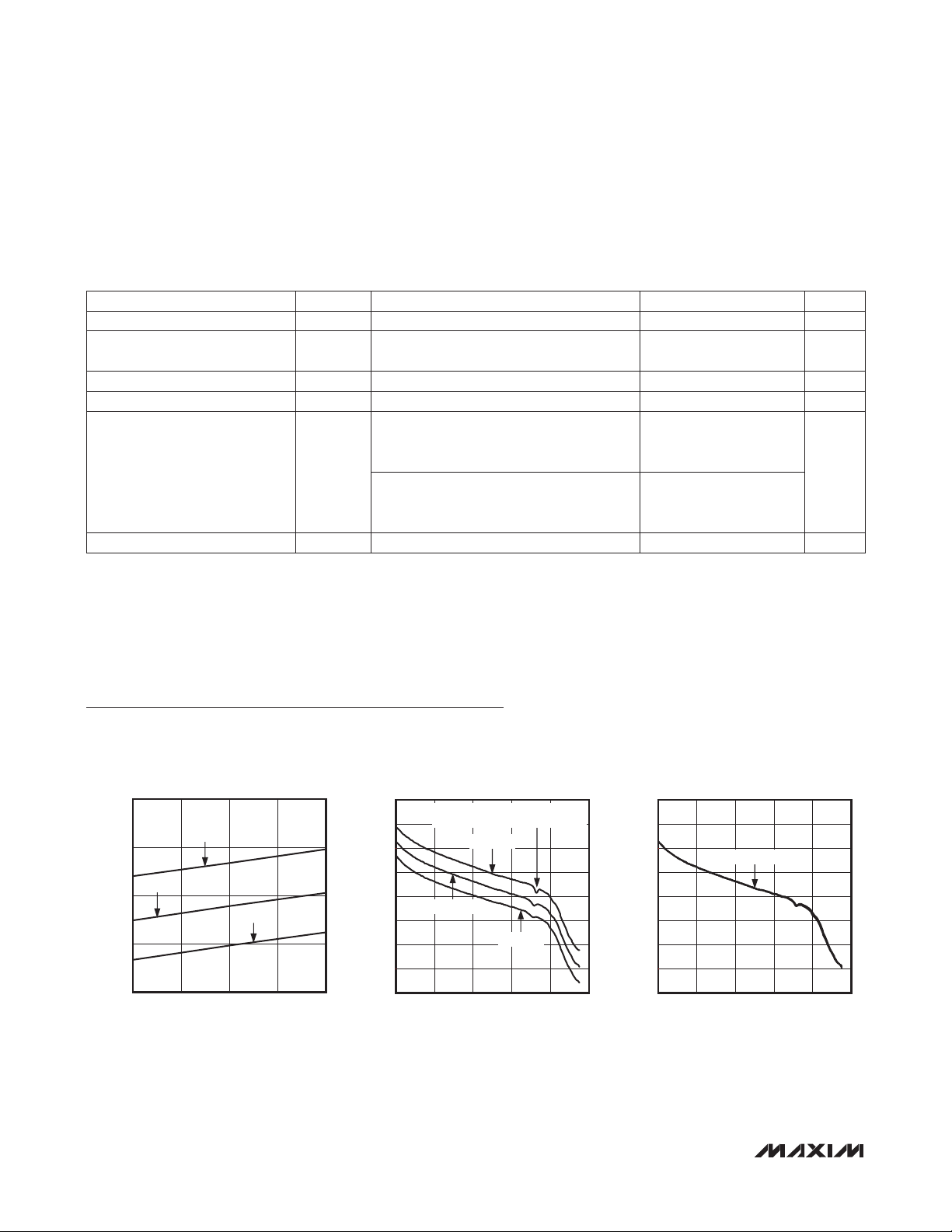
Typical Operating Characteristics
(Typical Application Circuit, VCC = V
CC_AMP_1
driven from 50I sources, AMPSET = 0, PD_1 = PD_2 = 0, P
170
SUPPLY CURRENT vs. V
160
TC = +25°C
150
SUPPLY CURRENT (mA)
140
130
4.750 5.250
TC = -40°C
TC = +85°C
VCC (V)
CC
5.1255.004.875
MAX2062 toc01
= V
CC_AMP_2
= V
= -20dBm, fRF = 350MHz, and TC = +25NC, unless otherwise noted.)
IN
= 5.0V, attenuators are set for maximum gain, RF ports are
CC_RG
GAIN vs. RF FREQUENCY
22
21
20
19
18
GAIN (dB)
17
16
15
14
NOTCH DUE TO SELF-RESONANCE OF
BIAS COIL. SEE TABLE 7.
TC = -40°C
TC = +25°C
TC = +85°C
50 1050
RF FREQUENCY (MHz)
22
GAIN vs. RF FREQUENCY
21
MAX2062 toc02
20
19
18
GAIN (dB)
17
16
15
850650250 450
14
50 1050
VCC = 4.75V, 5.00V, 5.25V
850650250 450
RF FREQUENCY (MHz)
dB
MAX2062 toc03
6 ______________________________________________________________________________________
Page 7
Dual 50MHz to 1000MHz High-Linearity,
Serial/Parallel-Controlled Analog/Digital VGA
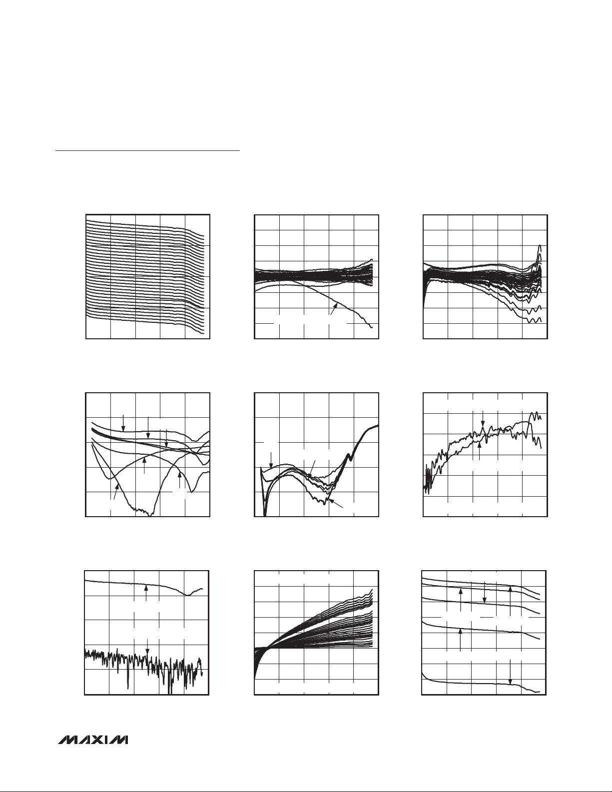
Typical Operating Characteristics (continued)
(Typical Application Circuit, VCC = V
CC_AMP_1
driven from 50I sources, AMPSET = 0, PD_1 = PD_2 = 0, P
= V
CC_AMP_2
= V
= -20dBm, fRF = 350MHz, and TC = +25NC, unless otherwise noted.)
IN
= 5.0V, attenuators are set for maximum gain, RF ports are
CC_RG
MAX2062
GAIN OVER DIGITAL ATTENUATOR
SETTING vs. RF FREQUENCY
22
12
2
-8
GAIN OVER DIGITAL ATTENUATOR SETTING (dB)
-18
50 1050
RF FREQUENCY (MHz)
850650450250
INPUT MATCH OVER DIGITAL ATTENUATOR
SETTING vs. RF FREQUENCY
0
0dB
-10
-20
-30
-40
2dB
-50
INPUT MATCH OVER DIGITAL ATTENUATOR SETTING (dB)
0 1000
1dB
8dB, 16dB
31dB
4dB
800600400200
RF FREQUENCY (MHz)
REVERSE ISOLATION OVER DIGITAL
ATTENUATOR SETTING vs. RF FREQUENCY
30
40
DIGITAL ATTENUATOR 0dB
50
DIGITAL ATTENUATOR 31dB
60
ATTENUATOR SETTING (dB)
70
REVERSE ISOLATION OVER DIGITAL
80
50 1050
RF FREQUENCY (MHz)
850650450250
DIGITAL ATTENUATOR RELATIVE
ERROR vs. RF FREQUENCY
1.00
0.75
MAX2062 toc04
0.50
0.25
0
-0.25
RELATIVE ERROR (dB)
-0.50
-0.75
-1.00
ERROR FROM 23dB TO 24dB
50 1050
RF FREQUENCY (MHz)
OUTPUT MATCH OVER DIGITAL
ATTENUATOR SETTING vs. RF FREQUENCY
0
MAX2062 toc07
-10
-20
2dB
0dB, 1dB, 4dB, 8dB
-30
-40
-50
0 1000
OUTPUT MATCH OVER DIGITAL ATTENUATOR SETTING (dB)
RF FREQUENCY (MHz)
DIGITAL ATTENUATOR PHASE CHANGE
BETWEEN STATES vs. RF FREQUENCY
50
REFERENCED TO HIGH GAIN STATE
40
MAX2062 toc10
30
20
10
0
-10
BETWEEN STATES (DEGREES)
DIGITAL ATTENUATOR PHASE CHANGE
-20
POSITIVE PHASE = ELECTRICALLY SHORTER
-30
50 1050
RF FREQUENCY (MHz)
850650250 450
16dB, 31dB
800600400200
850650250 450
DIGITAL ATTENUATOR ABSOLUTE
ERROR vs. RF FREQUENCY
1.00
0.75
MAX2062 toc05
0.50
0.25
0
-0.25
ABSOLUTE ERROR (dB)
-0.50
-0.75
-1.00
50 1050
RF FREQUENCY (MHz)
CHANNEL-TO-CHANNEL ISOLATION
vs. RF FREQUENCY
20
BOTH DIGITAL ATTENUATORS = 31dB
30
MAX2062 toc08
40
50
60
70
CHANNEL-TO-CHANNEL ISOLATION (dB)
80
BOTH DIGITAL ATTENUATORS = 0dB
BOTH ANALOG ATTENUATORS = 0dB
50 1050
RF FREQUENCY (MHz)
GAIN OVER ANALOG ATTENUATOR
SETTING vs. RF FREQUENCY
22
17
MAX2062 toc11
12
7
2
-3
-8
-13
GAIN OVER ANALOG ATTENUATOR SETTING (dB)
-18
50 1050
DAC CODE 64
DAC CODE 32
DAC CODE 128
RF FREQUENCY (MHz)
MAX2062 toc06
850650250 450
MAX2062 toc09
850650450250
MAX2062 toc12
DAC CODE 0
DAC CODE 255
850650250 450
_______________________________________________________________________________________ 7
Page 8
Dual 50MHz to 1000MHz High-Linearity,
Serial/Parallel-Controlled Analog/Digital VGA
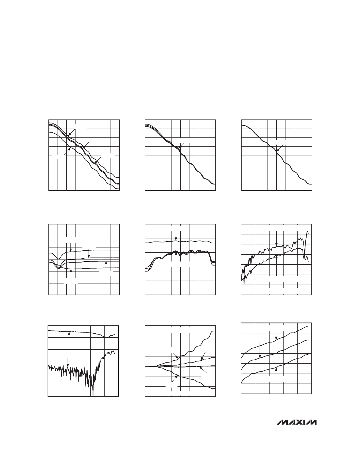
Typical Operating Characteristics (continued)
(Typical Application Circuit, VCC = V
CC_AMP_1
driven from 50I sources, AMPSET = 0, PD_1 = PD_2 = 0, P
= V
CC_AMP_2
= V
= -20dBm, fRF = 350MHz, and TC = +25NC, unless otherwise noted.)
IN
= 5.0V, attenuators are set for maximum gain, RF ports are
CC_RG
GAIN vs. ANALOG ATTENUATOR SETTING
22
MAX2062
17
12
7
2
1000MHz
GAIN (dB)
-3
-8
-13
-18
0 256
ANALOG ATTENUATOR SETTING (DAC CODE)
INPUT MATCH vs. ANALOG
ATTENUATOR SETTING
0
-5
-10
-15
INPUT MATCH (dB)
-20
-25
-30
50MHz
1000MHz
ANALOG ATTENUATOR SETTING (DAC CODE)
REVERSE ISOLATION OVER ANALOG
ATTENUATOR SETTING vs. RF FREQUENCY
30
40
50
60
70
ATTENUATOR SETTING (dB)
REVERSE ISOLATION OVER ANALOG
80
90
DAC CODE 0
DAC CODE 255
50 1050
RF FREQUENCY (MHz)
50MHz
200MHz
200MHz
350MHz
350MHz
850650450250
22419232 64 96 128 160
22419232 64 96 128 1600 256
GAIN vs. ANALOG ATTENUATOR SETTING
22
17
MAX2062 toc13
12
7
2
GAIN (dB)
-3
-8
-13
-18
0 256
ANALOG ATTENUATOR SETTING (DAC CODE)
0
MAX2062 toc16
-10
-20
-30
OUTPUT MATCH (dB)
-40
-50
ANALOG ATTENUATOR SETTING (DAC CODE)
vs. ANALOG ATTENUATOR SETTING
80
REFERENCED TO HIGH GAIN STATE
60
MAX2062 toc19
40
20
0
-20
S21 PHASE CHANGE (DEGREES)
-40
POSITIVE PHASE = ELECTRICALLY SHORTER
-60
ANALOG ATTENUATOR SETTING (DAC CODE)
RF = 350MHz
TC = -40°C, +25°C, +85°C
OUTPUT MATCH vs. ANALOG
ATTENUATOR SETTING
1000MHz
50MHz, 200MHz, 350MHz
S21 PHASE CHANGE
1000MHz
50MHz
350MHz
200MHz
22419232 64 96 128 160
22419232 64 96 128 1600 256
224 25619232 64 96 128 1600
GAIN vs. ANALOG ATTENUATOR SETTING
22
17
MAX2062 toc14
12
7
2
GAIN (dB)
-3
-8
-13
-18
0 256
ANALOG ATTENUATOR SETTING (DAC CODE)
CHANNEL-TO-CHANNEL ISOLATION
vs. RF FREQUENCY
10
BOTH ANALOG ATTENUATORS = CODE 255
20
MAX2062 toc17
30
40
50
60
BOTH ANALOG ATTENUATORS = CODE 0
70
CHANNEL-TO-CHANNEL ISOLATION (dB)
BOTH DIGITAL ATTENUATORS = 0dB
80
50 1050
RF FREQUENCY (MHz)
NOISE FIGURE vs. RF FREQUENCY
11
10
MAX2062 toc20
NOISE FIGURE (dB)
TC = +25°C
9
8
7
6
5
4
50 1050
RF FREQUENCY (MHz)
RF = 350MHz
MAX2062 toc15
VCC = 4.75V, 5.00V, 5.25V
22419232 64 96 128 160
MAX2062 toc18
850650450250
TC = +85°C
MAX2062 toc21
TC = -40°C
850650450250
8 ______________________________________________________________________________________
Page 9

Dual 50MHz to 1000MHz High-Linearity,
Serial/Parallel-Controlled Analog/Digital VGA
Typical Operating Characteristics (continued)
(Typical Application Circuit, VCC = V
CC_AMP_1
driven from 50I sources, AMPSET = 0, PD_1 = PD_2 = 0, P
= V
CC_AMP_2
= V
= -20dBm, fRF = 350MHz, and TC = +25NC, unless otherwise noted.)
IN
= 5.0V, attenuators are set for maximum gain, RF ports are
CC_RG
MAX2062
NOISE FIGURE vs. RF FREQUENCY
11
10
9
8
7
NOISE FIGURE (dB)
6
5
4
50 1050
VCC = 4.75V, 5.00V, 5.25V
RF FREQUENCY (MHz)
OUTPUT IP3 vs. RF FREQUENCY
50
45
40
35
OUTPUT IP3 (dBm)
30
25
20
TC = +85°C
TC = +25°C
50 1050
RF FREQUENCY (MHz)
TC = -40°C
P
OUT
OUTPUT IP3 vs. ANALOG
ATTENUATOR STATE
45
TC = -40°C LSB, USB
40
35
TC = +25°C LSB, USB
OUTPUT IP3 (dBm)
TC = +85°C LSB, USB
30
P
= -3dBm/TONE
OUT
850650450250
= 0dBm/TONE
850650450250
RF = 350MHz
21
MAX2062 toc22
19
(dBm)
17
1dB
15
OUTPUT P
13
11
50
45
MAX2062 toc25
40
35
OUTPUT IP3 (dBm)
30
25
20
70
MAX2062 toc28
60
50
2ND HARMONIC (dBc)
40
OUTPUT P
50 1050
vs. RF FREQUENCY
1dB
TC = -40°C
TC = +85°C
TC = +25°C
RF FREQUENCY (MHz)
850650450250
OUTPUT IP3 vs. RF FREQUENCY
P
= 0dBm/TONE
OUT
VCC = 5.25V
VCC = 4.75V
VCC = 5.00V
50 1050
RF FREQUENCY (MHz)
850650450250
2ND HARMONIC vs. RF FREQUENCY
P
= 3dBm
TC = +85°C
TC = +25°C
TC = -40°C
OUT
21
MAX2062 toc23
19
(dBm)
17
1dB
15
OUTPUT P
13
11
44
42
MAX2062 toc26
40
38
36
OUTPUT IP3 (dBm)
34
32
30
70
MAX2062 toc29
60
50
2ND HARMONIC (dBc)
40
OUTPUT P
VCC = 4.75V
50 1050
vs. RF FREQUENCY
1dB
VCC = 5.25V
VCC = 5.00V
RF FREQUENCY (MHz)
850650450250
OUTPUT IP3 vs. DIGITAL
ATTENUATOR STATE
RF = 350MHz
TC = -40°C USB
TC = +25°C LSB, USB
TC = +85°C LSB
TC = +85°C USB
0 28
DIGITAL ATTENUATOR STATE (dB)
TC = -40°C LSB
P
= -3dBm/TONE
OUT
2420161284
2ND HARMONIC vs. RF FREQUENCY
P
= 3dBm
OUT
VCC = 5.25V
VCC = 5.00V
VCC = 4.75V
MAX2062 toc24
MAX2062 toc27
MAX2062 toc30
25
0 210
ANALOG ATTENUATOR STATE (DAC CODE)
1681268442
_______________________________________________________________________________________ 9
30
50 1050
RF FREQUENCY (MHz)
850650450250
30
50 1050
RF FREQUENCY (MHz)
850650450250
Page 10

Dual 50MHz to 1000MHz High-Linearity,
Serial/Parallel-Controlled Analog/Digital VGA
Typical Operating Characteristics (continued)
(Typical Application Circuit, VCC = V
CC_AMP_1
driven from 50I sources, AMPSET = 0, PD_1 = PD_2 = 0, P
= V
CC_AMP_2
= V
= -20dBm, fRF = 350MHz, and TC = +25NC, unless otherwise noted.)
IN
= 5.0V, attenuators are set for maximum gain, RF ports are
CC_RG
2ND HARMONIC vs. DIGITAL
ATTENUATOR STATE
65
TC = +85°C
MAX2062
60
55
TC = -40°C
2ND HARMONIC (dBc)
50
45
0 28
DIGITAL ATTENUATOR STATE (dB)
3RD HARMONIC vs. RF FREQUENCY
100
90
80
70
3RD HARMONIC (dBc)
60
50
VCC = 5.25V
VCC = 4.75V
RF FREQUENCY (MHz)
TC = +25°C
VCC = 5.00V
P
= 0dBm
OUT
RF = 350MHz
2420161284
P
= 3dBm
OUT
850 105065045025050
MAX2062 toc31
2ND HARMONIC (dBc)
MAX2062 toc34
3RD HARMONIC (dBc)
2ND HARMONIC vs. ANALOG
ATTENUATOR STATE
70
65
TC = +25°C
60
55
50
45
ANALOG ATTENUATOR STATE (DAC CODE)
TC = +85°C
TC = -40°C
P
OUT
RF = 350MHz
168 21012684420
3RD HARMONIC vs. DIGITAL
ATTENUATOR STATE
85
TC = -40°C
80
75
70
0 28
TC = +25°C
TC = +85°C
DIGITAL ATTENUATOR STATE (dB)
P
OUT
RF = 350MHz
= 0dBm
= 0dBm
2420161284
100
90
MAX2062 toc32
80
70
3RD HARMONIC (dBc)
60
50
90
85
MAX2062 toc35
80
75
70
3RD HARMONIC (dBc)
65
60
3RD HARMONIC vs. RF FREQUENCY
P
= 3dBm
OUT
TC = -40°C
TC = +25°C
TC = +85°C
850 105065045025050
RF FREQUENCY (MHz)
3RD HARMONIC vs. ANALOG
ATTENUATOR STATE
P
= 0dBm
TC = -40°C
TC = +25°C
TC = +85°C
ANALOG ATTENUATOR STATE (DAC CODE)
OUT
RF = 350MHz
168 21012684420
MAX2062 toc33
MAX2062 toc36
70
TC = +85°C
60
50
OIP2 (dBm)
TC = -40°C
40
30
50 1050
RF FREQUENCY (MHz)
P
TC = +25°C
= 0dBm/TONE
OUT
OIP2 vs. RF FREQUENCY
70
MAX2062 toc37
60
50
OIP2 (dBm)
40
30
850650450250
VCC = 5.25V
VCC = 4.75V
50 1050
RF FREQUENCY (MHz)
P
= 0dBm/TONE
OUT
VCC = 5.00V
MAX2062 toc38
850650450250
OIP2 vs. RF FREQUENCY
OIP2 vs. DIGITAL ATTENUATOR STATE
65
60
TC = +85°C
55
OIP2 (dBm)
50
TC = -40°C
45
40
0 28
DIGITAL ATTENUATOR STATE (dB)
10 _____________________________________________________________________________________
P
= -3dBm/TONE
OUT
TC = +25°C
RF = 350MHz
2420161284
MAX2062 toc39
Page 11

Dual 50MHz to 1000MHz High-Linearity,
Serial/Parallel-Controlled Analog/Digital VGA
Typical Operating Characteristics (continued)
(Typical Application Circuit, VCC = V
CC_AMP_1
driven from 50I sources, AMPSET = 0, PD_1 = PD_2 = 0, P
= V
CC_AMP_2
= V
= -20dBm, fRF = 350MHz, and TC = +25NC, unless otherwise noted.)
IN
= 5.0V, attenuators are set for maximum gain, RF ports are
CC_RG
MAX2062
OIP2 vs. ANALOG ATTENUATOR STATE
60
TC = +85°C
55
50
OIP2 (dBm)
45
40
35
TC = -40°C
0 210
ANALOG ATTENUATOR STATE (DAC CODE)
P
OUT
TC = +25°C
DAC VOLTAGE DRIFT vs. DAC CODE
0.05
0.04
0.03
0.02
0.01
-0.01
-0.02
DAC VOLTAGE DRIFT (V)
-0.03
-0.04
-0.05
TC CHANGED FROM +25°C TO -40°C
0
TC CHANGED FROM +25°C TO +85°C
0 256
DAC CODE
GAIN vs. RF FREQUENCY
(DIGITAL ATTENUATOR ONLY)
0
= -3dBm/TONE
RF = 350MHz
1681268442
224192128 16064 9632
3.0
2.5
MAX2062 toc40
2.0
1.5
DAC VOLTAGE (V)
1.0
0.5
0
0 256
0.0100
0.0075
MAX2062 toc43
0.0050
0.0025
0
-0.0025
DAC VOLTAGE DRIFT (V)
-0.0050
-0.0075
0.0100
0 256
0
DAC VOLTAGE vs. DAC CODE
TC = -40°C, +25°C, +85°C
224192160128966432
DAC CODE
DAC VOLTAGE DRIFT vs. DAC CODE
VCC CHANGED FROM 5.00V TO 5.25V
VCC CHANGED FROM 5.00V TO 4.75V
22419232 64 96 128 160
DAC CODE
GAIN vs. RF FREQUENCY
(ANALOG ATTENUATOR ONLY)
MAX2062 toc41
DAC VOLTAGE (V)
MAX2062 toc44
GAIN (dB)
DAC VOLTAGE vs. DAC CODE
3.0
2.5
2.0
1.5
1.0
V
= 4.75V, 5.00V, 5.25V
0.5
0
0 256
CC
DAC CODE
GAIN vs. RF FREQUENCY
(DIGITAL ATTENUATOR ONLY)
0
-1
-2
-3
-4
-5
50 1050
TC = -40°C
TC = +85°C
RF FREQUENCY (MHz)
TC = +25°C
850650450250
GAIN vs. RF FREQUENCY
(ANALOG ATTENUATOR ONLY)
0
MAX2062 toc42
224192160128966432
MAX2062 toc45
-1
-2
GAIN (dB)
-3
-4
-5
50 1050
VCC = 4.75V, 5.00V, 5.25V
RF FREQUENCY (MHz)
______________________________________________________________________________________ 11
MAX2062 toc46
-1
-2
GAIN (dB)
-3
-4
850650450250
-5
50 1050
TC = -40°C
TC = +85°C
RF FREQUENCY (MHz)
TC = +25°C
850650450250
MAX2062 toc47
-1
-2
GAIN (dB)
-3
-4
-5
50 1050
V
= 4.75V, 5.00V, 5.25V
CC
RF FREQUENCY (MHz)
MAX2062 toc48
850650450250
Page 12

Dual 50MHz to 1000MHz High-Linearity,
Serial/Parallel-Controlled Analog/Digital VGA
Typical Operating Characteristics (continued)
(Typical Application Circuit, VCC = V
CC_AMP_1
driven from 50I sources, AMPSET = 1, PD_1 = PD_2 = 0, P
= V
CC_AMP_2
= V
= -20dBm, fRF = 350MHz, and TC = +25NC, unless otherwise noted.)
IN
= 3.3V, attenuators are set for maximum gain, RF ports are
CC_RG
120
MAX2062
110
100
90
80
SUPPLY CURRENT (mA)
70
60
3.1 3.5
TC = -40°C
TC = +25°C
TC = +85°C
VCC (V)
INPUT MATCH OVER DIGITAL ATTENUATOR
SETTING vs. RF FREQUENCY
SUPPLY CURRENT vs. V
0
0dB
-10
-20
-30
-40
-50
INPUT MATCH OVER DIGITAL ATTENUATOR SETTING (dB)
0 1000
1dB
31dB
2dB
RF FREQUENCY (MHz)
OUTPUT MATCH vs. ANALOG
ATTENUATOR SETTING
0
-10
-20
-30
OUTPUT MATCH (dB)
-40
1000MHz
50MHz, 200MHz, 350MHz
CC
3.43.33.2
VCC = 3.3V
8dB, 16dB
800600400200
VCC = 3.3V
4dB
22
MAX2062 toc49
21
20
19
18
GAIN (dB)
17
16
15
14
TC = -40°C
TC = +25°C
TC = +85°C
50 1050
RF FREQUENCY (MHz)
OUTPUT MATCH OVER DIGITAL
ATTENUATOR SETTING vs. RF FREQUENCY
GAIN vs. RF FREQUENCY
0
MAX2062 toc52
-10
-20
-30
-40
-50
0 1000
OUTPUT MATCH OVER DIGITAL ATTENUATOR SETTING (dB)
2dB
0dB, 1dB, 4dB, 8dB
16dB, 31dB
RF FREQUENCY (MHz)
NOISE FIGURE vs. RF FREQUENCY
11
MAX2062 toc55
NOISE FIGURE (dB)
VCC = 3.3V
10
9
8
7
6
5
TC = +85°C
TC = -40°C
TC = +25°C
VCC = 3.3V
850650250 450
VCC = 3.3V
800600400200
MAX2062 toc50
GAIN (dB)
MAX2062 toc53
INPUT MATCH (dB)
MAX2062 toc56
NOISE FIGURE (dB)
22
21
20
19
18
17
16
15
14
50 1050
VCC = 3.465V
VCC = 3.135V
VCC = 3.30V
850650250 450
RF FREQUENCY (MHz)
INPUT MATCH vs. ANALOG
ATTENUATOR SETTING
GAIN vs. RF FREQUENCY
0
-5
-10
-15
-20
-25
-30
0 256
50MHz
1000MHz
ANALOG ATTENUATOR SETTING (DAC CODE)
VCC = 3.3V
200MHz
350MHz
NOISE FIGURE vs. RF FREQUENCY
11
V
10
9
8
7
6
5
VCC = 3.135V
VCC = 3.465V
CC
MAX2062 toc51
MAX2062 toc54
224192160128966432
= 3.30V
MAX2062 toc57
-50
0 256
ANALOG ATTENUATOR SETTING (DAC CODE)
4
224192160128966432
50 1050
RF FREQUENCY (MHz)
850650450250
4
50 1050
RF FREQUENCY (MHz)
12 _____________________________________________________________________________________
850650450250
Page 13

Dual 50MHz to 1000MHz High-Linearity,
Serial/Parallel-Controlled Analog/Digital VGA
Typical Operating Characteristics (continued)
(Typical Application Circuit, VCC = V
CC_AMP_1
driven from 50I sources, AMPSET = 1, PD_1 = PD_2 = 0, P
= V
CC_AMP_2
= V
= -20dBm, fRF = 350MHz, and TC = +25NC, unless otherwise noted.)
IN
= 3.3V, attenuators are set for maximum gain, RF ports are
CC_RG
MAX2062
OUTPUT P
16
14
(dBm)
12
1dB
10
OUTPUT P
8
6
50 1050
vs. RF FREQUENCY
1dB
TC = -40°C
TC = +85°C
RF FREQUENCY (MHz)
TC = +25°C
OUTPUT IP3 vs. RF FREQUENCY
40
35
30
25
OUTPUT IP3 (dBm)
20
15
10
VCC = 3.465V
50 1050
RF FREQUENCY (MHz)
P
VCC = 3.30V
VCC = 3.135V
= 0dBm/TONE
OUT
2ND HARMONIC vs. RF FREQUENCY
65
55
45
2ND HARMONIC (dBc)
35
TC = +85°C
TC = +25°C
TC = -40°C
VCC = 3.3V
850650450250
850650450250
P
= 3dBm
OUT
VCC = 3.3V
16
MAX2062 toc58
14
(dBm)
12
1dB
10
OUTPUT P
8
6
34
MAX2062 toc61
32
30
28
OUTPUT IP3 (dBm)
26
24
65
MAX2062 toc64
55
45
2ND HARMONIC (dBc)
35
OUTPUT P
50 1050
1dB
vs. RF FREQUENCY
VCC = 3.30V
VCC = 3.465V
RF FREQUENCY (MHz)
VCC = 3.135V
850650450250
OUTPUT IP3
vs. DIGITAL ATTENUATOR STATE
P
RF = 350MHz
TC = -40°C LSB, USB
TC = +25°C LSB, USB
0 28
DIGITAL ATTENUATOR STATE (dB)
= -3dBm/TONE
OUT
VCC = 3.3V
TC = +85°C LSB, USB
2420161284
2ND HARMONIC vs. RF FREQUENCY
P
= 3dBm
OUT
VCC = 3.465V
VCC = 3.135V
VCC = 3.30V
40
35
MAX2062 toc59
30
25
OUTPUT IP3 (dBm)
20
15
10
35
MAX2062 toc62
30
OUTPUT IP3 (dBm)
25
20
70
MAX2062 toc65
60
50
2ND HARMONIC (dBc)
OUTPUT IP3 vs. RF FREQUENCY
P
= 0dBm/TONE
TC = -40°C
TC = +85°C
50 1050
RF FREQUENCY (MHz)
OUT
VCC = 3.3V
TC = +25°C
850650450250
OUTPUT IP3
vs. ANALOG ATTENUATOR STATE
P
= -3dBm/TONE
RF = 350MHz
TC = -40°C LSB, USB
TC = +25°C LSB, USB
TC = +85°C LSB, USB
0 210
ANALOG ATTENUATOR STATE (DAC CODE)
OUT
VCC = 3.3V
1681268442
2ND HARMONIC
vs. DIGITAL ATTENUATOR STATE
P
RF = 350MHz
TC = +85°C
TC = +25°C
TC = -40°C
= 0dBm
OUT
VCC = 3.3V
MAX2062 toc60
MAX2062 toc63
MAX2062 toc66
25
50 1050
RF FREQUENCY (MHz)
850650450250
______________________________________________________________________________________ 13
25
50 1050
RF FREQUENCY (MHz)
850650450250
40
0 28
DIGITAL ATTENUATOR STATE (dB)
2420161284
Page 14

Dual 50MHz to 1000MHz High-Linearity,
Serial/Parallel-Controlled Analog/Digital VGA
Typical Operating Characteristics (continued)
(Typical Application Circuit, VCC = V
CC_AMP_1
driven from 50I sources, AMPSET = 1, PD_1 = PD_2 = 0, P
= V
CC_AMP_2
= V
= -20dBm, fRF = 350MHz, and TC = +25NC, unless otherwise noted.)
IN
= 3.3V, attenuators are set for maximum gain, RF ports are
CC_RG
2ND HARMONIC
vs. ANALOG ATTENUATOR STATE
70
RF = 350MHz
MAX2062
60
50
2ND HARMONIC (dBc)
40
75
70
65
60
3RD HARMONIC (dBc)
55
TC = +85°C
TC = +25°C
0 210
ANALOG ATTENUATOR STATE (DAC CODE)
3RD HARMONIC
vs. DIGITAL ATTENUATOR STATE
RF = 350MHz
TC = +25°C
TC = -40°C
TC = +85°C
P
OUT
VCC = 3.3V
TC = -40°C
P
OUT
VCC = 3.3V
= 0dBm
1681268442
= 0dBm
80
MAX2062 toc67
70
60
3RD HARMONIC (dBc)
50
40
75
MAX2062 toc70
70
65
60
3RD HARMONIC (dBc)
55
3RD HARMONIC vs. RF FREQUENCY
P
= 3dBm
OUT
VCC = 3.3V
TC = -40°C
TC = +25°C
TC = +85°C
50 1050
RF FREQUENCY (MHz)
850650450250
3RD HARMONIC
vs. ANALOG ATTENUATOR STATE
P
RF = 350MHz
TC = -40°C
TC = +25°C
OUT
VCC = 3.3V
TC = +85°C
= 0dBm
80
MAX2062 toc68
70
60
3RD HARMONIC (dBc)
50
40
70
60
MAX2062 toc71
50
OIP2 (dBm)
40
30
3RD HARMONIC vs. RF FREQUENCY
P
= 3dBm
OUT
VCC = 3.30V
VCC = 3.135V
VCC = 3.465V
50 1050
RF FREQUENCY (MHz)
850650450250
OIP2 vs. RF FREQUENCY
P
= 0dBm/TONE
OUT
TC = +85°C
TC = +25°C
TC = -40°C
VCC = 3.3V
MAX2062 toc69
MAX2062 toc72
MAX2062 toc74
20
50 1050
RF FREQUENCY (MHz)
OIP2 vs. ANALOG ATTENUATOR STATE
70
RF = 350MHz
TC = +85°C
60
50
OIP2 (dBm)
40
30
TC = -40°C
0 210
ANALOG ATTENUATOR STATE (DAC CODE)
50
0 28
DIGITAL ATTENUATOR STATE (dB)
OIP2 vs. RF FREQUENCY
70
60
50
OIP2 (dBm)
40
30
20
VCC = 3.465V
VCC = 3.135V
50 1050
RF FREQUENCY (MHz)
P
= 0dBm/TONE
OUT
VCC = 3.30V
2420161284
50
0 210
ANALOG ATTENUATOR STATE (DAC CODE)
1681268442
OIP2 vs. DIGITAL ATTENUATOR STATE
70
RF = 350MHz
MAX2062 toc73
OIP2 (dBm)
850650450250
TC = +85°C
60
50
40
TC = -40°C
30
0 28
DIGITAL ATTENUATOR STATE (dB)
TC = +25°C
P
= -3dBm/TONE
OUT
VCC = 3.3V
2420161284
14 _____________________________________________________________________________________
TC = +25°C
P
= -3dBm/TONE
OUT
850650450250
VCC = 3.3V
1681268442
MAX2062 toc75
Page 15

Dual 50MHz to 1000MHz High-Linearity,
Serial/Parallel-Controlled Analog/Digital VGA
Pin Configuration
TOP VIEW
MAX2062
V
CC_AMP_1
A_ATT_OUT_1
A_VCTL_1
AA_SP
A_ATT_IN_1
D4_1
D_ATT_OUT_1
D3_1
D2_1
D1_1
D0_1
GND
AMP_IN_1
PD_1
GND
35
34 33 32 31 30 29 28 27
36
37
38
39
40
41
42
43
44
45
46
47
48
+
2
3 4 5 6 7 8 9 10
1
GND
STA_A_1
D_ATT_IN_1
AMP_OUT_1
GND
MAX2062
DAT
STA_B_1
AMPSET
CLK
AMP_OUT_2
REG_OUT
CS
CC_RG
V
GND
STA_B_2
AMP_IN_2
PD_2
26
11
STA_A_2
D_ATT_IN_2
GND
25
V
24
CC_AMP_2
A_ATT_OUT_2
23
22
A_VCTL_2
21
DA_SP
A_ATT_IN_2
20
D4_2
19
18
D_ATT_OUT_2
17
D3_2
16
D2_2
D1_2
15
D0_2
14
EP
13
GND
12
GND
TQFN
Pin Description
PIN NAME FUNCTION
1, 12, 13, 25,
28, 33, 36, 48
2 D_ATT_IN_1
3 STA_A_1
4 STA_B_1
5 DAT SPI Data Digital Input
6 CLK SPI Clock Digital Input
7
8 V
GND Ground
5-Bit Digital Attenuator Input (50I), Path 1. Requires a DC-blocking capacitor.
Digital Attenuator Preprogrammed Attenuation-State Logic Input, Path 1
State A State B Digital Attenuator
Logic = 0 Logic = 0 Preprogrammed State 1
Logic = 1 Logic = 0 Preprogrammed State 2
Logic = 0 Logic = 1 Preprogrammed State 3
Logic = 1 Logic = 1 Preprogrammed State 4
CS
CC_RG
SPI Chip-Select Digital Input
Regulator Supply Input. Connect to a 3.3V or 5V external power supply. V
powers all circuits
CC_RG
except for the driver amplifiers. Bypass with a 10nF capacitor as close as possible to the pin.
______________________________________________________________________________________ 15
Page 16

Dual 50MHz to 1000MHz High-Linearity,
Serial/Parallel-Controlled Analog/Digital VGA
Pin Description (continued)
PIN NAME FUNCTION
9 STA_B_2
MAX2062
10 STA_A_2
11 D_ATT_IN_2
14 D0_2 1dB Attenuator Logic Input, Path 2. Logic 0 = disable, logic 1 = enable.
15 D1_2 2dB Attenuator Logic Input, Path 2. Logic 0 = disable, logic 1 = enable.
16 D2_2 4dB Attenuator Logic Input, Path 2. Logic 0 = disable, logic 1 = enable.
17 D3_2 8dB Attenuator Logic Input, Path 2. Logic 0 = disable, logic 1 = enable.
18 D_ATT_OUT_2
19 D4_2 16dB Attenuator Logic Input, Path 2. Logic 0 = disable, logic 1 = enable.
20 A_ATT_IN_2
21 DA_SP
22 A_VCTL_2
23 A_ATT_OUT_2
24 V
26 AMP_IN_2
27 PD_2 Power-Down, Path 2. See Table 2 for operation details.
29 AMP_OUT_2
30 REG_OUT
31 AMPSET
32 AMP_OUT_1
34 PD_1 Power-Down, Path 1. See Table 2 for operation details.
35 AMP_IN_1
37 V
38 A_ATT_OUT_1
39 A_VCTL_1
CC_AMP_2
CC_AMP_1
Digital Attenuator Preprogrammed Attenuation-State Logic Input, Path 2
State A State B Digital Attenuator
Logic = 0 Logic = 0 Preprogrammed State 1
Logic = 1 Logic = 0 Preprogrammed State 2
Logic = 0 Logic = 1 Preprogrammed State 3
Logic = 1 Logic = 1 Preprogrammed State 4
5-Bit Digital Attenuator Input (50I), Path 2. Requires a DC-blocking capacitor.
5-Bit Digital Attenuator Output (50I), Path 2. Requires a DC-blocking capacitor. Connect to
A_ATT_IN_2 through a 1000pF capacitor.
Analog Attenuator Input (50I), Path 2. Requires a DC-blocking capacitor. Connect to
D_ATT_OUT_2 through a 1000pF capacitor.
Digital Attenuator Serial/Parallel Control Select. Set DA_SP to logic 1 to select serial control.
Set DA_SP to logic 0 to select parallel control.
Analog Attenuator Voltage Control Input, Path 2. Bypass to ground with a 150pF capacitor
if on-chip DAC is used (AA_SP = 1).
Analog Attenuator Output (50I), Path 2. Requires a DC-blocking capacitor. Connect to
AMP_IN_2 through a 1000pF capacitor.
Driver Amplifier Supply Voltage Input, Path 2. Bypass with a 10nF capacitor as close as
possible to the pin.
Driver Amplifier Input (50I), Path 2. Requires a DC-blocking capacitor. Connect to
A_ATT_OUT_2 through a 1000pF capacitor.
Driver Amplifier Output (50I), Path 2. Connect a pullup inductor from AMP_OUT_2 to V
Regulator Output. Bypass with 1FF capacitor.
Driver Amplifier Bias Setting for 3.3V Operation. Set to logic 1 for 3.3V operation on pins
V
CC_AMP_1
Driver Amplifier Output (50I), Path 1. Connect a pullup inductor from AMP_OUT_1 to V
Driver Amplifier Input (50I), Path 1. Requires a DC-blocking capacitor. Connect to
A_ATT_OUT_1 through a 1000pF capacitor.
Driver Amplifier Supply Voltage Input, Path 1. Bypass with a 10nF capacitor as close as
possible to the pin.
Analog Attenuator Output (50I), Path 1. Requires a DC-blocking capacitor. Connect to
AMP_IN_1 through a 1000pF capacitor.
Analog Attenuator Voltage Control Input, Path 1. Bypass to ground with a 150pF capacitor
if on-chip DAC is used (AA_SP = 1).
and V
CC_AMP_2
. Set to logic 0 for 5V operation.
CC_.
CC_.
16 _____________________________________________________________________________________
Page 17

Dual 50MHz to 1000MHz High-Linearity,
Serial/Parallel-Controlled Analog/Digital VGA
Pin Description (continued)
PIN NAME FUNCTION
DAC Enable/Disable Logic Input for Analog Attenuators. Set AA_SP to logic 1 to enable on-chip
40 AA_SP
41 A_ATT_IN_1
42 D4_1 16dB Attenuator Logic Input, Path 1. Logic 0 = disable, logic 1 = enable.
43 D_ATT_OUT_1
44 D3_1 8dB Attenuator Logic Input, Path 1. Logic 0 = disable, logic 1 = enable.
45 D2_1 4dB Attenuator Logic Input, Path 1. Logic 0 = disable, logic 1 = enable.
46 D1_1 2dB Attenuator Logic Input, Path 1. Logic 0 = disable, logic 1 = enable.
47 D0_1 1dB Attenuator Logic Input, Path 1. Logic 0 = disable, logic 1 = enable.
— EP
DAC circuit and digital SPI control. Set AA_SP to logic 0 to disable DAC circuit and digital SPI
control. When AA_SP = 0, use analog control lines (A_VCTL_1 and A_VCTL_2).
Analog Attenuator Input (50I), Path 1. Requires a DC-blocking capacitor. Connect to
D_ATT_OUT_1 through a 1000pF capacitor.
5-Bit Digital Attenuator Output (50I), Path 1. Requires a DC-blocking capacitor. Connect to
A_ATT_IN_1 through a 1000pF capacitor.
Exposed Pad. Internally connected to GND. Connect to GND for proper RF performance and
enhanced thermal dissipation.
MAX2062
Detailed Description
The MAX2062 high-linearity analog/digital VGA is a
general-purpose, high-performance amplifier designed
to interface with 50I systems operating in the 50MHz to
1000MHz frequency range.
Each channel of the device integrates one digital attenuator and one analog attenuator to provide 64dB of total gain
control, as well as a driver amplifier optimized to provide
high gain, high IP3, low NF, and low power consumption.
Each digital attenuator is controlled as a slave peripheral using either the SPI-compatible interface, or a 5-bit
parallel bus with 31dB total adjustment range in 1dB
steps. An added feature allows rapid-fire gain selection
among each of the four steps, preprogrammed by the
user through the SPI-compatible interface. A separate
2-pin control lets the user quickly access any one of four
customized attenuation states without reprogramming
the SPI bus. Each analog attenuator is controlled using
an external voltage or through the SPI-compatible interface using an on-chip 8-bit DAC. See the Applications
Information section for attenuator programming details.
Because each of the three stages in the separate signal
paths has its own RF input and RF output, this component can be configured to either optimize NF (amplifier
configured first), OIP3 (amplifier last), or a compromise
of NF and OIP3. The device’s performance features
include 24dB amplifier gain (amplifier only), 7.3dB NF
at maximum gain (includes attenuator insertion losses),
and a high OIP3 level of +41dBm. Each of these features
makes the device an ideal VGA for multipath receiver
and transmitter applications.
In addition, the device operates from a single +5V
supply with full performance, or a +3.3V supply for an
enhanced power-savings mode with lower performance.
The device is available in a compact 48-pin TQFN package (7mm x 7mm) with an exposed pad. Electrical performance is guaranteed over the extended temperature
range (T
= -40NC to +85NC).
C
Analog and 5-Bit Digital Attenuator Control
The device integrates two analog attenuators and two
5-bit digital attenuators to achieve a high level of dynamic range. Each analog attenuator has a 33dB range
and is controlled using an external voltage or through
the 3-wire SPI interface using an on-chip 8-bit DAC.
Each digital attenuator has a 31dB control range, a 1dB
step size, and is programmed either through the 3-wire
SPI or through a separate 5-bit parallel bus. See the
Applications Information section and Table 1 for attenuator programming details. The attenuators can be used
for both static and dynamic power control.
Note that when the analog attenuators are controlled
by the DACs through the SPI bus, the DAC output
voltage shows on pins A_VCTL_1 and A_VCTL_2 (pins
39 and 22, respectively). Therefore, in SPI mode, the
A_VCTL_1 and A_VCTL_2 pins must only connect to the
resistor and capacitor to ground, as shown in the Typical
Application Circuit.
______________________________________________________________________________________ 17
Page 18

Dual 50MHz to 1000MHz High-Linearity,
Serial/Parallel-Controlled Analog/Digital VGA
Table 1. Control Logic
AA_SP ANALOG ATTENUATOR D/A CONVERTER
0 Controlled by external control voltage Disabled
1 Controlled by on-chip DAC
DA_SP DIGITAL ATTENUATOR
MAX2062
0 Parallel controlled
1 SPI controlled (control voltages show up on the parallel control pins)
Enabled (DAC output voltage shows on A_VCTL__ pins);
DAC uses on-chip voltage reference
Driver Amplifier
Each path of the device includes a high-performance
driver with a fixed gain of 24dB. The driver amplifier
circuits are optimized for high linearity for the 50MHz to
1000MHz frequency range.
Applications Information
Operating Modes
The device features an optional +3.3V supply voltage operation with reduced linearity performance. The
AMPSET pin needs to be biased accordingly in each
mode, as listed in Table 2. In addition, the driver amplifiers
can be shut down independently to conserve DC power.
See the biasing scheme outlined in Table 2 for details.
SPI Interface and Attenuator Settings
The digital attenuators can be programmed through the
3-wire SPI/MICROWIREK-compatible serial interface
using 5-bit words. Fifty-six bits of data are shifted in
MSB first and are framed by CS. The first 28 bits set the
first attenuator and the following 28 bits set the second
attenuator. When CS is low, the clock is active and data
is shifted on the rising edge of the clock. When CS transitions high, the data is latched and the attenuator setting
changes (Figure 1). See Table 3 for details on the SPI
data format.
Table 2. Operating Modes
RESULT VCC (V) AMPSET PD_1 PD_2
All on
AMP1 off
AMP2 on
AMP1 on
AMP2 off
All off
5 0 0 0
3.3 1 0 0
5 0 1 0
3.3 1 1 0
5 0 0 1
3.3 1 0 1
5 0 1 1
3.3 1 1 1
Path 1 DAC and Digital Attenuator Programming
D0:D7 Sent to DAC register
D0 = LSB, D7 = MSB
D8:D12 Preprogrammed Attenuation State 1
D8 = 1dB bit, D9 = 2dB Bit, D10 = 4dB bit,
D11 = 8dB bit, D12 = 16dB bit
D13:D17 Preprogrammed Attenuation State 2
D13 = 1dB bit, D14 = 2dB bit, D15 = 4dB
bit, D16 = 8dB bit, D17 = 16dB bit
D18:D22 Preprogrammed Attenuation State 3
D18 = 1dB bit, D19 = 2dB bit, D20 = 4dB
bit, D21 = 8dB bit, D22 = 16dB bit
D23:D27 Preprogrammed Attenuation State 4
D23 = 1dB bit, D24 = 2dB bit, D25 = 4dB
bit, D26 = 8dB bit, D27 = 16dB bit
Path 2 DAC and Digital Attenuator Programming
D28:D35 Sent to DAC register
D28 = LSB, D35 = MSB
D36:D40 Preprogrammed Attenuation State 1
D36 = 1dB bit, D37 = 2dB bit, D38 = 4dB
bit, D39 = 8dB bit, D40 = 16dB bit
D41:D45 Preprogrammed Attenuation State 2
D41 = 1dB bit, D42 = 2dB bit, D43 = 4dB
bit, D44 = 8dB bit, D45 = 16dB bit
D46:D50 Preprogrammed Attenuation State 3
D46 = 1dB bit, D47 = 2dB bit, D48 = 4dB
bit, D49 = 8dB bit, D50 = 16dB bit
D51:D55 Preprogrammed Attenuation State 4
D51 = 1dB bit, D52 = 2dB bit, D53 = 4dB
bit, D54 = 8dB bit, D55 = 16dB bit
MICROWIRE is a trademark of National Semiconductor Corp.
18 _____________________________________________________________________________________
Page 19

Dual 50MHz to 1000MHz High-Linearity,
Serial/Parallel-Controlled Analog/Digital VGA
Table 3. SPI Data Format
FUNCTION BIT DESCRIPTION
D55 (MSB) 16dB step (MSB of the 5-bit word used to program the Path 2 digital attenuator state 4)
Digital Attenuator State 4
(Path 2)
Digital Attenuator State 3
(Path 2)
Digital Attenuator State 2
(Path 2)
Digital Attenuator State 1
(Path 2)
On-Chip DAC
(Path 2)
Digital Attenuator State 4
(Path 1)
Digital Attenuator State 3
(Path 1)
D54 8dB step
D53 4dB step
D52 2dB step
D51 1dB step
D50 16dB step (MSB of the 5-bit word used to program the Path 2 digital attenuator state 3)
D49 8dB step
D48 4dB step
D47 2dB step
D46 1dB step
D45 16dB step (MSB of the 5-bit word used to program the Path 2 digital attenuator state 2)
D44 8dB step
D43 4dB step
D42 2dB step
D41 1dB step
D40 16dB step (MSB of the 5-bit word used to program the Path 2 digital attenuator state 1)
D39 8dB step
D38 4dB step
D37 2dB step
D36 1dB step
D35 Bit 7 (MSB) of on-chip DAC used to program the Path 2 analog attenuator
D34 Bit 6 of DAC
D33 Bit 5 of DAC
D32 Bit 4 of DAC
D31 Bit 3 of DAC
D30 Bit 2 of DAC
D29 Bit 1 of DAC
D28 Bit 0 (LSB) of DAC
D27 16dB step (MSB of the 5-bit word used to program the Path 1 digital attenuator state 4)
D26 8dB step
D25 4dB step
D24 2dB step
D23 1dB step
D22 16dB step (MSB of the 5-bit word used to program the Path 1 digital attenuator state 3)
D21 8dB step
D20 4dB step
D19 2dB step
D18 1dB step
MAX2062
______________________________________________________________________________________ 19
Page 20

Dual 50MHz to 1000MHz High-Linearity,
Serial/Parallel-Controlled Analog/Digital VGA
Table 3. SPI Data Format (continued)
FUNCTION BIT DESCRIPTION
D17 16dB step (MSB of the 5-bit word used to program the Path 1 digital attenuator state 2)
Digital Attenuator State 2
(Path 1)
MAX2062
Digital Attenuator State 1
(Path 1)
On-Chip DAC
(Path 1)
D16 8dB step
D15 4dB step
D14 2dB step
D13 1dB step
D12 16dB step (MSB of the 5-bit word used to program the Path 1 digital attenuator state 1)
D11 8dB step
D10 4dB step
D9 2dB step
D8 1dB step
D7 Bit 7 (MSB) of on-chip DAC used to program the Path 1 analog attenuator
D6 Bit 6 of DAC
D5 Bit 5 of DAC
D4 Bit 4 of DAC
D3 Bit 3 of DAC
D2 Bit 2 of DAC
D1 Bit 1 of DAC
D0 (LSB) Bit 0 (LSB) of DAC
Figure 1. SPI Timing Diagram
MSB LSB
DATA
CLOCK
CS
NOTES:
DN D1 D0D(N-1)
t
CS
t
EWS
DATA ENTERED ON CLOCK RISING EDGE.
ATTENUATOR REGISTER STATE CHANGE ON CS RISING EDGE.
N = NUMBER OF DATA BITS.
t
t
CH
CW
t
ES
t
EW
20 _____________________________________________________________________________________
Page 21

Dual 50MHz to 1000MHz High-Linearity,
Serial/Parallel-Controlled Analog/Digital VGA
Attenuator and DAC Operation
The two analog attenuators are controlled by an external
control voltage applied at A_VCTL_1 and A_VCTL_2
(pins 39 and 22) or by the on-chip 8-bit DACs, while
the digital attenuators are controlled through the SPIcompatible interface or through two independent,
parallel 5-bit buses. The DAC enable/disable logic-input
pin (AA_SP) and digital attenuator SPI/parallel control
selection logic-input pin (DA_SP) determine how the
attenuators are controlled.
Digital Attenuator Settings
Using the Parallel Control Bus
To capitalize on its fast 25ns switching capability, the
device offers a supplemental 5-bit parallel control interface. The digital logic attenuator control pins (D0_–D4_)
enable the attenuator stages (see Tables 3 and 4).
Direct access to these 5-bit buses enables the user to
avoid any programming delays associated with the SPI
interface. One of the limitations of any SPI bus is the
speed at which commands can be clocked into each
peripheral device. By offering direct access to the 5-bit
parallel interface, the user can quickly shift between
digital attenuator states needed for critical fast-attack
automatic gain control (AGC) applications.
Note that when the digital attenuators are controlled by
the SPI bus, the control voltages of each digital attenuator appears on the five parallel control pins (pins 14–17
and 19 for digital attenuator 2, pins 42 and 44–47 for
MAX2062
digital attenuator 1). When the digital attenuators are
in SPI mode, the parallel control pins must be left
unconnected.
Rapid-Fire Preprogrammed
Attenuation States
The device has an added feature that provides rapidfire gain selection among four preprogrammed attenuation steps. As with the supplemental 5-bit buses
previously mentioned, this rapid-fire gain selection allows
the user to quickly access any one of four customized
digital attenuation states without incurring the delays
associated with reprogramming the device through the
SPI bus.
The switching speed is comparable to that achieved
using the supplemental 5-bit parallel buses. However, by
employing this specific feature, the digital attenuator I/O
is further reduced by a factor of either 5 or 2.5 (5 control
bits vs. 1 or 2, respectively), depending on the number
of states desired.
The user can employ the STA_A_1 and STA_B_1
(STA_A_2 and STA_B_2 for digital attenuator 2) logicinput pins to apply each step as required (see Tables
5 and 6). Toggling just the STA_A_1 pin (1 control bit)
yields two preprogrammed attenuation states; toggling
both the STA_A_1 and STA_B_1 pins together (2 control
bits) yields four preprogrammed attenuation states.
Table 4. Digital Attenuator Settings (Parallel Control, DA_SP = 0)
INPUT LOGIC = 0 (OR GROUND) LOGIC = 1
D0 Disable 1dB attenuator Enable 1dB attenuator
D1 Disable 2dB attenuator Enable 2dB attenuator
D2 Disable 4dB attenuator Enable 4dB attenuator
D3 Disable 8dB attenuator Enable 8dB attenuator
D4 Disable 16dB attenuator Enable 16dB attenuator
Table 5. Programmed Attenuation State
Settings for Attenuator 1 (DA_SP = 1)
STA_A_1 STA_B_1
0 0 Preprogrammed attenuation state 1
1 0 Preprogrammed attenuation state 2
0 1 Preprogrammed attenuation state 3
1 1 Preprogrammed attenuation state 4
*Defined by SPI programming bits D8:D27 (see Table 3 for
details).
______________________________________________________________________________________ 21
SETTING FOR DIGITAL
ATTENUATOR 1*
Table 6. Programmed Attenuation State
Settings for Attenuator 2 (DA_SP = 1)
STA_A_2 STA_B_2
0 0 Preprogrammed attenuation state 1
1 0 Preprogrammed attenuation state 2
0 1 Preprogrammed attenuation state 3
1 1 Preprogrammed attenuation state 4
**Defined by SPI programming bits D36:D55 (see Table 3 for
details).
SETTING FOR DIGITAL
ATTENUATOR 2**
Page 22

Dual 50MHz to 1000MHz High-Linearity,
Serial/Parallel-Controlled Analog/Digital VGA
As an example, assume that the AGC application
requires a static attenuation adjustment to trim out gain
inconsistencies within a receiver lineup. The same AGC
circuit can also be called upon to dynamically attenuate an unwanted blocker signal that could desensitize
The sequence to be used is:
1) Power supply
2) Control lines
the receiver and lead to an ADC overdrive condition.
In this example, the device would be preprogrammed
(through the SPI bus) with two customized attenuation
MAX2062
states—one to address the static gain-trim adjustment,
the second to counter the unwanted blocker condition.
Toggling just the STA_A_1 control bit enables the user to
switch quickly between the static and dynamic attenuation settings with only one I/O pin.
If desired, the user can also program two additional
attenuation states by using the STA_B_1 control bit as a
second I/O pin. These two additional attenuation settings
are useful for software-defined radio applications where
multiple static gain settings are needed to account for different frequencies of operation, or where multiple dynamic
attenuation settings are needed to account for different
The pin configuration of the device is optimized to facilitate a very compact physical layout of the device and its
associated discrete components. The exposed pad (EP)
of the device’s 48-pin TQFN-EP package provides a low
thermal-resistance path to the die. It is important that
the PCB on which the device is mounted be designed
to conduct heat from the EP. In addition, provide the EP
with a low inductance path to electrical ground. The EP
MUST be soldered to a ground plane on the PCB, either
directly or through an array of plated via holes. The layout of the PCB should include proper top-layer ground
shielding to isolate the amplifier’s inputs and outputs
from each other. Shielding between the paths (inputs and
outputs) is important for channel-to-channel isolation.
blocker levels (as defined by multiple wireless standards).
Table 7. Typical Application Circuit Component Values
DESIGNATION QTY DESCRIPTION COMPONENT SUPPLIER
C1, C2, C5, C6, C8,
C9, C12, C13
C3, C10 2
C4, C7, C11,
C14, C16
C15 1
L1, L2* 2
R1, R2 2
U1 1
*Select the inductors to ensure that self-resonance of the inductors is outside the band of operation.
8
5
1000pF ceramic capacitors (0402)
GRM1555C1H102J
150pF ceramic capacitors (0402)
GRM1555C1H151J
10nF ceramic capacitors (0402)
GRM155R71E103K
1FF ceramic capacitor (0603)
GRM188R71C105K
820nH inductors (1008)
Coilcraft 1008CS-821XJLC
47.5kI resistors (0402)
48 TQFN-EP (7mm x 7mm)
Maxim MAX2062ETM
Murata Electronics North America, Inc.
Murata Electronics North America, Inc.
Murata Electronics North America, Inc.
Murata Electronics North America, Inc.
Coilcraft, Inc.
—
Maxim Integrated Products, Inc.
Power-Supply Sequencing
Layout Considerations
22 _____________________________________________________________________________________
Page 23

Dual 50MHz to 1000MHz High-Linearity,
Serial/Parallel-Controlled Analog/Digital VGA
Typical Application Circuit
MAX2062
ANALOG
ATTENUATOR
CONTROL 1
C3
GND
AMP_IN_2
25272930
26
12
11
GND
D_ATT_IN_2
RF
OUTPUT 2
C13
V
CC_AMP_2
24
A_ATT_OUT_2
23
A_VCTL_2
22
DA_SP
21
A_ATT_IN_2
20
D4_2
19
D_ATT_OUT_2
18
D3_2
17
D2_2
16
D1_2
15
D0_2
14
GND
13
V
CC
C12C5 C11C4
ANALOG
ATTENUATOR
CONTROL 2
R2
C9
C10
RF
OUTPUT 1
C6
V
CC
GND
36
V
CC_AMP_1
A_ATT_OUT_1
A_VCTL_1
AA_SP_1
R1
C2
A_ATT_IN_1
D_ATT_OUT_1
D4_1
D3_1
D2_1
D1_1
D0_1
GND
37
38
39
40
41
42
43
44
45
46
47
48
+
1
GND
L1 L2
AMP_IN_1
GND
PD_1
35
33313234
ACTIVE
BIAS
ANALOG
ATTENUATOR
1
EXPOSED
PAD
DIGITAL
ATTENUATOR
1
2
3 4 5 6 7 8 9 10
STA_B_1
STA_A_1
D_ATT_IN_1
C7
V
CC
C15
AMP_OUT_2
REG_OUT
AMPSET
AMP_OUT_1
AMP AMP
DAC 2DAC 1
MAX2062
SPI
CS
CLK
DAT
CC_RG
V
C14
PD_2
GND
28
ACTIVE
BIAS
ANALOG
ATTENUATOR
2
DIGITAL
ATTENUATOR
2
STA_A_2
STA_B_2
C1
RF
INPUT 1
Chip Information
PROCESS: SiGe BiCMOS
______________________________________________________________________________________ 23
V
CC
C16
C8
RF
INPUT 2
Package Information
For the latest package outline information and land patterns,
go to www.maxim-ic.com/packages. Note that a “+”, “#”, or
“-” in the package code indicates RoHS status only. Package
drawings may show a different suffix character, but the drawing
pertains to the package regardless of RoHS status.
PACKAGE
TYPE
48 TQFN-EP T4877+7
PACKAGE
CODE
OUTLINE
NO.
LAND PATTERN
NO.
21-0144 90-0133
Page 24

Dual 50MHz to 1000MHz High-Linearity,
Serial/Parallel-Controlled Analog/Digital VGA
Revision History
REVISION
NUMBER
0 9/10 Initial release —
1 11/10 Updated Output Voltage specification 5
MAX2062
REVISION
DATE
DESCRIPTION
PAGES
CHANGED
Maxim cannot assume responsibility for use of any circuitry other than circuitry entirely embodied in a Maxim product. No circuit patent licenses are implied.
Maxim reserves the right to change the circuitry and specifications without notice at any time.
24 Maxim Integrated Products, 120 San Gabriel Drive, Sunnyvale, CA 94086 408-737-7600
©
2010 Maxim Integrated Products Maxim is a registered trademark of Maxim Integrated Products, Inc.
 Loading...