

Page 1
General Description
The MAX2056 general-purpose, high-performance variable-gain amplifier (VGA) is designed to operate in the
800MHz to 1000MHz frequency range*. This device features 15.5dB of gain, 4.5dB of noise figure, and an output 1dB compression point of 23.5dBm. The MAX2056
also provides an exceptionally high OIP3 level of
39dBm, which is maintained over the entire attenuation
range. In addition, the on-chip analog attenuators yield
infinite control and high attenuation accuracy over
selectable 22dB or 44dB control ranges. Each of these
features makes the MAX2056 an ideal VGA for cellular
band GSM, cdma2000®, W-CDMA, and iDEN®transmitter and power amplifier AGC circuits.
The MAX2056 is pin compatible with the MAX2057
1700MHz to 2500MHz VGA, making this family of
amplifiers ideal for applications where a common PC
board layout is used for both frequency bands.
The MAX2056 operates from a single +5V supply and is
available in a compact 36-pin thin QFN package (6mm
x 6mm x 0.8mm) with an exposed pad. Electrical performance is guaranteed over the extended -40°C to
+85°C temperature range.
Applications
GSM 850/GSM 900 2G and 2.5G EDGE BaseStation Transmitters and Power Amplifiers
Cellular cdmaOne™, cdma2000, and Integrated
Digital Enhanced Network (iDEN) Base-Station
Transmitters and Power Amplifiers
W-CDMA 850MHz and Other 3G Base-Station
Transmitters and Power Amplifiers
Transmitter Gain Control
Receiver Gain Control
Broadband Systems
Automatic Test Equipment
Digital and Spread-Spectrum Communication
Systems
Microwave Terrestrial Links
cdmaOne is a trademark of CDMA Development Group.
cdma2000 is a registered trademark of Telecommunications
Industry Association.
iDEN is a registered trademark of Motorola, Inc.
Features
♦ 800MHz to 1000MHz RF Frequency Range*
♦ 39dBm Constant OIP3 (Over All Gain Settings)
♦ 23.5dBm Output 1dB Compression Point
♦ 15.5dB Typical Gain at Maximum Gain Setting
♦ 0.15dB Gain Flatness Over 100MHz Bandwidth
♦ 4.5dB Noise Figure at Maximum Gain Setting
(Using 1 Attenuator)
♦ Two Gain-Control Ranges: 22dB and 44dB
♦ Analog Gain Control
♦ Single +5V Supply Voltage
♦ Pin Compatible with MAX2057, 1700MHz to
2500MHz RF VGA
♦ External Current-Setting Resistors Provide Option
for Operating VGA in Reduced-Power/ReducedPerformance Mode
♦ Lead-Free Package Available
*Note: Operation beyond this range is possible, but has not been
characterized.
MAX2056
800MHz to 1000MHz Variable-Gain
Amplifier with Analog Gain Control
________________________________________________________________ Maxim Integrated Products 1
Ordering Information
19-3508; Rev 0; 2/05
For pricing, delivery, and ordering information, please contact Maxim/Dallas Direct! at
1-888-629-4642, or visit Maxim’s website at www.maxim-ic.com.
EVALUATION KIT
AVAILABLE
PART
TEMP
RANGE
PIN-PACKAGE
PKG
CODE
MAX2056ETX
T3666-2
MAX2056ETX-T
6m m x 6m m
T3666-2
MAX2056ETX+D
T3666-2
M AX 2056E TX + TD
T3666-2
**EP = Exposed paddle.
+ = Lead (Pb) free.
D = Dry pack.
T = Tape-and-reel package.
Pin Configuration/Functional Diagram appears at end of data
sheet.
- 40°C to + 85°C
- 40°C to + 85°C
- 40°C to + 85°C
- 40°C to + 85°C
36 Thin QFN -EP **
6m m x 6m m
36 Thin QFN -EP **
36 Thin QFN -EP **
6m m x 6m m
36 Thin QFN -EP **
6m m x 6m m
Page 2
MAX2056
800MHz to 1000MHz Variable-Gain
Amplifier with Analog Gain Control
2 _______________________________________________________________________________________
ABSOLUTE MAXIMUM RATINGS
Stresses beyond those listed under “Absolute Maximum Ratings” may cause permanent damage to the device. These are stress ratings only, and functional
operation of the device at these or any other conditions beyond those indicated in the operational sections of the specifications is not implied. Exposure to
absolute maximum rating conditions for extended periods may affect device reliability.
VCCto GND...........................................................-0.3V to +5.5V
V
CNTL
to GND (with VCCapplied)................................0 to 4.75V
Current into V
CNTL
Pin (VCCgrounded) .............................40mA
All Other Pins to GND.................................-0.3V to (V
CC
+ 0.3V)
RF Input Power (IN, IN_A, ATTN_OUT, OUT_A) ............+20dBm
RF Input Power (AMP_IN)...............................................+12dBm
θJA(natural convection)...................................................35°C/W
θ
JA
(1m/s airflow) .............................................................31°C/W
θ
JA
(2.5m/s airflow) ..........................................................29°C/W
θ
JC
(junction to exposed paddle) ....................................10°C/W
Operating Temperature Range ...........................-40°C to +85°C
Storage Temperature Range .............................-65°C to +150°C
Junction Temperature......................................................+150°C
Lead Temperature (soldering, 10s) .................................+300°C
AC ELECTRICAL CHARACTERISTICS
(Typical Operating Circuit with one attenuator connected, VCC= +4.75V to +5.25V, TA= -40°C to +85°C, unless otherwise noted.
Typical values are at V
CC
= +5.0V, R1 = 1.2kΩ, R2 = 3.92kΩ, P
OUT
= +5dBm, fIN= 900MHz, V
CNTL
= 1V, 50Ω system impedance,
second attenuator is not connected, T
A
= +25°C, unless otherwise noted.) (Note 3)
PARAMETER CONDITIONS
UNITS
Frequency Range
MHz
Gain TA = +25°C
dB
V
CNTL
= 1V
V
CNTL
= 1.8V
V
CNTL
= 2.6V
TA = +25°C to -40°C
V
CNTL
= 3.5V
V
CNTL
= 1V
V
CNTL
= 1.8V
V
CNTL
= 2.6V
Maximum Gain Variation
T
A
= +25°C to +85°C
V
CNTL
= 3.5V
dB
Reverse Isolation 29 dB
Noise Figure (Note 4) 4.5 dB
Output 1dB Compression Point
dBm
Output 2nd-Order Intercept Point
From maximum gain to 15dB attenuation,
measured at f
1
+ f2 (Note 5)
dBm
Output 3rd-Order Intercept Point
dBm
DC ELECTRICAL CHARACTERISTICS
(VCC= +4.75V to +5.25V, no RF signals applied, all input and output ports terminated with 50Ω, TA= -40°C to +85°C, unless otherwise noted. Typical values are at V
CC
= +5.0V, TA= +25°C, unless otherwise noted.)
PARAMETER CONDITIONS
UNITS
Supply Voltage
5
V
Supply Current R1 = 1.2kΩ, R2 = 3.92kΩ (Note 1)
167 mA
R
SET1
Current R1 = 1.2kΩ (Note 1) 1 mA
R
SET2
Current R2 = 3.92kΩ (Note 1)
mA
Gain-Control Voltage Range (Note 2) 1.0 4.5 V
Gain-Control Pin Input Resistance V
CNTL
= 1V to 4.5V
kΩ
MIN TYP MAX
4.75
136
0.33
5.25
250 500
From maximum gain to 15dB attenuation (Note 5) +39
MIN TYP MAX
800 1000
15.5
+0.82
+0.26
+0.25
-0.18
-0.51
-0.11
-0.16
+0.09
+23.5
+54
Page 3
MAX2056
800MHz to 1000MHz Variable-Gain
Amplifier with Analog Gain Control
_______________________________________________________________________________________ 3
AC ELECTRICAL CHARACTERISTICS (continued)
(Typical Operating Circuit with one attenuator connected, VCC= +4.75V to +5.25V, TA= -40°C to +85°C, unless otherwise noted.
Typical values are at V
CC
= +5.0V, R1 = 1.2kΩ, R2 = 3.92kΩ, P
OUT
= +5dBm, fIN= 900MHz, V
CNTL
= 1V, 50Ω system impedance,
second attenuator is not connected, T
A
= +25°C, unless otherwise noted.) (Note 3)
Note 1: Total supply current reduces as R1 and R2 are increased.
Note 2: Operating outside this range for extended periods may affect device reliability. Limit pin input current to 40mA when V
CC
is
not present.
Note 3: All limits include external component losses, unless otherwise noted.
Note 4: Noise figure increases by approximately 1dB for every 1dB of gain reduction.
Note 5: f
1
= 900MHz, f2= 901MHz, +5dBm/tone at OUT.
Note 6: Switching time is measured from 50% of the control signal to when the RF output settles to ±1dB.
PARAMETER CONDITIONS
MIN
TYP
MAX
UNITS
TA = +25°C to +85°C
Output 3rd-Order Intercept Point
Variation Over Temperature
T
A
= +25°C to -40°C
dB
2nd Harmonic
From maximum gain to 15dB attenuation, P
OUT
=
+5dBm
-55 dBc
3rd Harmonic
From maximum gain to 15dB attenuation, P
OUT
=
+5dBm
-68 dBc
One attenuator
RF Gain-Control Range
f
RF
= 800MHz to 1000MHz,
V
CNTL
= 1V to 4.5V
Two attenuators
dB
RF Gain-Control Slope
dB/V
Maximum RF Gain-Control Slope Maximum slope vs. gain-control voltage
dB/V
Gain Flatness Over 100MHz Bandwidth
Peak-to-peak for all settings
dB
Attenuator Switching Time 15dB attenuation change (Note 6)
ns
Attenuator Insertion Loss Second attenuator (IN_A, OUT_A) 1.7 dB
Input Return Loss Entire band, all gain settings 15 dB
Output Return Loss Entire band, all gain settings 15 dB
Group Delay Input/output 50Ω lines de-embedded
ps
Group Delay Flatness Over 100MHz
Bandwidth
Peak to peak
ps
Group Delay Change vs. Gain Control V
CNTL
= 1V to 4V
ps
Insertion Phase Change vs. Gain Control
V
CNTL
= 1V to 4V 20
degrees
-0.46
+1.35
18.3 22.3
36.6 44.6
-10.7
-17.2
0.15
500
600
100
100
Page 4
MAX2056
800MHz to 1000MHz Variable-Gain
Amplifier with Analog Gain Control
4 _______________________________________________________________________________________
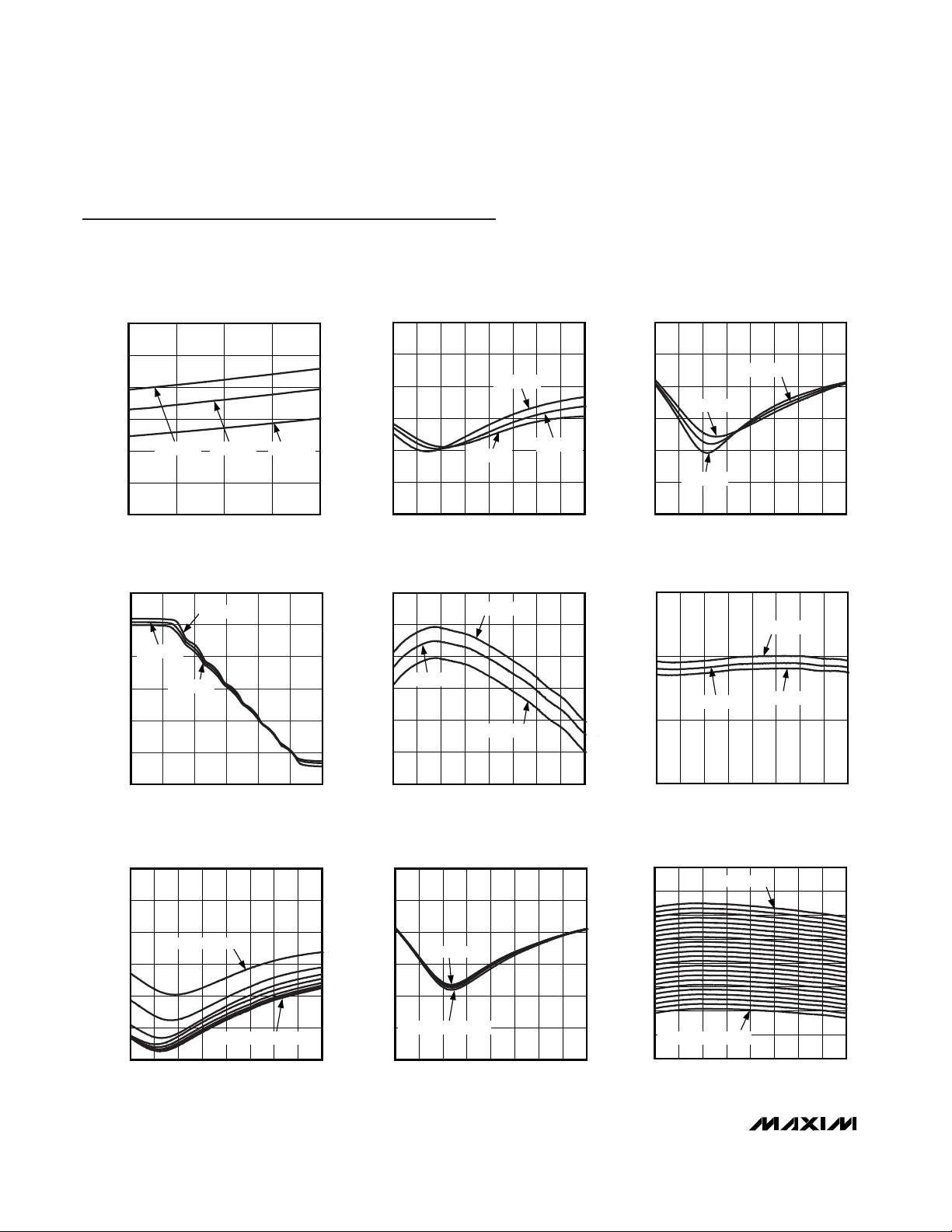
Typical Operating Characteristics
One Attenuator Configuration
(Typical Application Circuit with one attenuator connected, VCC= +5.0V, R1 = 1.2kΩ, R2 = 3.92kΩ, fIN= 900MHz maximum gain
setting, P
OUT
= +5dBm, linearity measured at P
OUT
= +5dBm/tone, TA= +25°C, unless otherwise noted.)
100
120
110
140
130
150
160
4.750 5.0004.875 5.125 5.250
SUPPLY CURRENT vs. V
CC
MAX2056 toc01
VCC (V)
SUPPLY CURRENT (mA)
TA = +85°C
TA = +25°C
TA = -40°C
30
25
20
15
10
5
0
700 900800 1000 1100 1200 1300 1400 1500
INPUT RETURN LOSS
vs. RF FREQUENCY
MAX2056 toc02
RF FREQUENCY (MHz)
INPUT RETURN LOSS (dB)
TA = +85°C
TA = +25°C
TA = -40°C
MAX2056 toc03
TA = +85°C
TA = +25°C
TA = -40°C
30
25
20
15
10
5
0
700 900800 1000 1100 1200 1300 1400 1500
OUTPUT RETURN LOSS
vs. RF FREQUENCY
RF FREQUENCY (MHz)
OUTPUT RETURN LOSS (dB)
GAIN vs. V
CNTL
MAX2056 toc04
V
CNTL
(V)
GAIN (dB)
3.53.02.52.01.5
-5
0
5
10
15
20
-10
1.0 4.0
TA = +85°C
TA = +25°C
TA = -40°C
11
12
13
14
15
16
17
GAIN vs. RF FREQUENCY
MAX2056 toc05
GAIN (dB)
TA = +85°C
TA = +25°C
TA = -40°C
700 900800 1000 1100 1200 1300 1400 1500
RF FREQUENCY (MHz)
20
25
30
35
REVERSE ISOLATION
vs. RF FREQUENCY
MAX2056 toc06
ISOLATION (dB)
TA = +85°C
TA = +25°C
TA = -40°C
700 900800 1000 1100 1200 1300 1400 1500
RF FREQUENCY (MHz)
30
25
20
15
10
5
0
INPUT RETURN LOSS
vs. RF FREQUENCY
MAX2056 toc07
INPUT RETURN LOSS (dB)
700 900800 1000 1100 1200 1300 1400 1500
RF FREQUENCY (MHz)
MAXIMUM GAIN
21dB GAIN REDUCTION
MAX2056 toc08
30
25
20
15
10
5
0
OUTPUT RETURN LOSS
vs. RF FREQUENCY
OUTPUT RETURN LOSS (dB)
700 900800 1000 1100 1200 1300 1400 1500
RF FREQUENCY (MHz)
MAXIMUM GAIN
21dB GAIN REDUCTION
-17
-7
-12
3
-2
8
13
18
23
MAX2056 toc09
GAIN (dB)
GAIN vs. RF FREQUENCY
700 900800 1000 1100 1200 1300 1400 1500
RF FREQUENCY (MHz)
MAXIMUM GAIN
22dB GAIN REDUCTION
Page 5

MAX2056
800MHz to 1000MHz Variable-Gain
Amplifier with Analog Gain Control
_______________________________________________________________________________________ 5
20
30
25
40
35
45
50
55
60
MAX2056 toc10
REVERSE ISOLATION (dB)
REVERSE ISOLATION
vs. RF FREQUENCY
700 900800 1000 1100 1200 1300 1400 1500
RF FREQUENCY (MHz)
21dB GAIN REDUCTION
MAXIMUM GAIN
2
3
5
4
6
7
NOISE FIGURE vs. RF FREQUENCY
MAX2056 toc11
RF FREQUENCY (MHz)
NOISE FIGURE (dB)
800 900850 950 1000
TA = +85°C
TA = +25°C
TA = -40°C
MAX2056 toc12
2
3
5
4
6
7
NOISE FIGURE vs. RF FREQUENCY
RF FREQUENCY (MHz)
NOISE FIGURE (dB)
800 900850 950 1000
VCC = 5.25V
VCC = 4.75V
VCC = 5.00V
36
37
39
38
40
41
OUTPUT IP3 vs. FREQUENCY
MAX2056 toc13
OUTPUT IP3 (dBm)
RF FREQUENCY (MHz)
800 900850 950 1000
TA = +85°C
TA = +25°C
TA = -40°C
MAX2056 toc14
36
37
39
38
40
41
OUTPUT IP3 vs. FREQUENCY
OUTPUT IP3 (dBm)
RF FREQUENCY (MHz)
800 900850 950 1000
VCC = 5.25V
VCC = 4.75V
VCC = 5.00V
20
30
25
40
35
45
50
025
INPUT IP3 vs. ATTENUATION
MAX2056 toc15
ATTENUATION (dB)
INPUT IP3 (dBm)
1051520
TA = +85°C
TA = +25°C
TA = -40°C
MAX2056 toc16
20
30
25
40
35
45
50
025
OUTPUT IP3 vs. ATTENUATION
ATTENUATION (dB)
OUTPUT IP3 (dBm)
1051520
TA = +85°C
TA = +25°C
TA = -40°C
40
38
36
34
32
-6 3-3 0 6 9 12
OUTPUT IP3 vs. OUTPUT POWER
MAX2056 toc17
OUTPUT POWER PER TONE (dBm)
OUTPUT IP3 (dBm)
40
45
55
50
60
65
OUTPUT IP2 vs. RF FREQUENCY
MAX2056 toc18
RF FREQUENCY (MHz)
OUTPUT IP2 (dBm)
800 900850 950 1000
TA = +85°C
TA = +25°C
TA = -40°C
Typical Operating Characteristics (continued)
One Attenuator Configuration
(Typical Application Circuit with one attenuator connected, VCC= +5.0V, R1 = 1.2kΩ, R2 = 3.92kΩ, fIN= 900MHz maximum gain
setting, P
OUT
= +5dBm, linearity measured at P
OUT
= +5dBm/tone, TA= +25°C, unless otherwise noted.)
Page 6

MAX2056
800MHz to 1000MHz Variable-Gain
Amplifier with Analog Gain Control
6 _______________________________________________________________________________________
45
50
60
55
65
70
MAX2056 toc19
OUTPUT IP2 vs. RF FREQUENCY
RF FREQUENCY (MHz)
OUTPUT IP2 (dBm)
800 900850 950 1000
VCC = 5.25V
VCC = 4.75V
VCC = 5.00V
35
45
40
55
50
60
65
025
INPUT IP2 vs. ATTENUATION
MAX2056 toc20
ATTENUATION (dB)
INPUT IP2 (dBm)
1051520
TA = +85°C
TA = +25°C
TA = -40°C
MAX2056 toc21
35
45
40
55
50
60
65
025
OUTPUT IP2 vs. ATTENUATION
ATTENUATION (dB)
OUTPUT IP2 (dBm)
1051520
TA = +85°C
TA = +25°C
TA = -40°C
20
22
21
24
23
25
26
800 900850 950 1000
OUTPUT P1dB vs. RF FREQUENCY
MAX2056 toc22
RF FREQUENCY (MHz)
OUTPUT P1dB (dBm)
TA = +85°C
TA = +25°C
TA = -40°C
MAX2056 toc23
20
22
21
24
23
25
26
800 900850 950 1000
OUTPUT P1dB vs. RF FREQUENCY
RF FREQUENCY (MHz)
OUTPUT P1dB (dBm)
VCC = 5.25V
VCC = 4.75V
VCC = 5.00V
Typical Operating Characteristics (continued)
One Attenuator Configuration
(Typical Application Circuit with one attenuator connected, VCC= +5.0V, R1 = 1.2kΩ, R2 = 3.92kΩ, fIN= 900MHz maximum gain
setting, P
OUT
= +5dBm, linearity measured at P
OUT
= +5dBm/tone, TA= +25°C, unless otherwise noted.)
Page 7

MAX2056
800MHz to 1000MHz Variable-Gain
Amplifier with Analog Gain Control
_______________________________________________________________________________________ 7
40
30
35
20
25
15
10
5
0
700 900 1000800 1100 1200 1300 1400 1500
INPUT RETURN LOSS
vs. RF FREQUENCY
MAX2056 toc24
RF FREQUENCY (MHz)
INPUT RETURN LOSS (dB)
TA = +85°C
TA = +25°C
TA = -40°C
30
25
20
15
10
5
0
MAX2056 toc25
700 900 1000800 1100 1200 1300 1400 1500
OUTPUT RETURN LOSS
vs. RF FREQUENCY
RF FREQUENCY (MHz)
OUTPUT RETURN LOSS (dB)
TA = +85°C
TA = +25°C
TA = -40°C
-25
-35
1.0 1.5 2.0 2.5 3.0 3.5 4.0
-5
-15
5
15
GAIN vs. V
CNTL
MAX2056 toc26
V
CNTL
(V)
GAIN (dB)
TA = +85°C
TA = +25°C
TA = -40°C
7
9
13
11
15
17
700 900 1000800 1100 1200 1300 1400 1500
GAIN vs. RF FREQUENCY
MAX2056 toc27
RF FREQUENCY (MHz)
GAIN (dB)
TA = +85°C
TA = +25°C
TA = -40°C
35
30
25
20
MAX2056 toc28
ISOLATION (dB)
700 900 1100 1300 1500
REVERSE ISOLATION
vs. RF FREQUENCY
RF FREQUENCY (MHz)
TA = +85°C
TA = +25°C
TA = -40°C
MAX2056 toc29
30
25
20
15
10
5
0
INPUT RETURN LOSS
vs. RF FREQUENCY
INPUT RETURN LOSS (dB)
700 900800 1000 1100 1200 1300 1400 1500
RF FREQUENCY (MHz)
MAXIMUM GAIN
42dB GAIN REDUCTION
MAX2056 toc30
30
25
20
15
10
5
0
OUTPUT RETURN LOSS
vs. RF FREQUENCY
OUTPUT RETURN LOSS (dB)
700 900800 1000 1100 1200 1300 1400 1500
RF FREQUENCY (MHz)
MAXIMUM GAIN
42dB GAIN REDUCTION
-45
-35
-15
-25
5
15
-5
25
MAX2056 toc31
GAIN (dB)
GAIN vs. RF FREQUENCY
700 900800 1000 1100 1200 1300 1400 1500
RF FREQUENCY (MHz)
44dB GAIN REDUCTION
MAXIMUM GAIN
Typical Operating Characteristics
Two Attenuator Configuration
(Typical Application Circuit with two attenuators connected, VCC= +5.0V, R1 = 1.2kΩ, R2 = 3.92kΩ, fIN= 900MHz maximum gain
setting, P
OUT
= +5dBm, linearity measured at P
OUT
= +5dBm/tone, TA= +25°C, unless otherwise noted.)
Page 8

MAX2056
800MHz to 1000MHz Variable-Gain
Amplifier with Analog Gain Control
8 _______________________________________________________________________________________
20
40
30
60
50
70
80
MAX2056 toc32
REVERSE ISOLATION (dB)
REVERSE ISOLATION
vs. RF FREQUENCY
700 900 1100 1300 1500
RF FREQUENCY (MHz)
42dB GAIN REDUCTION
MAXIMUM GAIN
4
5
7
6
8
9
MAX2056 toc33
NOISE FIGURE vs. RF FREQUENCY
RF FREQUENCY (MHz)
NOISE FIGURE (dB)
800 900850 950 1000
TA = +85°C
TA = +25°C
TA = -40°C
36
37
39
38
40
41
MAX2056 toc34
OUTPUT IP3 (dBm)
OUTPUT IP3 vs. RF FREQUENCY
RF FREQUENCY (MHz)
800 900850 950 1000
TA = +85°C
TA = +25°C
TA = -40°C
40
45
55
50
60
65
MAX2056 toc35
OUTPUT IP2 (dBm)
OUTPUT IP2 vs. RF FREQUENCY
RF FREQUENCY (MHz)
800 900850 950 1000
TA = +85°C
TA = +25°C
TA = -40°C
Typical Operating Characteristics (continued)
Two Attenuator Configuration
(Typical Application Circuit with two attenuators connected, VCC= +5.0V, R1 = 1.2kΩ, R2 = 3.92kΩ, fIN= 900MHz maximum gain
setting, P
OUT
= +5dBm, linearity measured at P
OUT
= +5dBm/tone, TA= +25°C, unless otherwise noted.)
Page 9

MAX2056
800MHz to 1000MHz Variable-Gain
Amplifier with Analog Gain Control
_______________________________________________________________________________________ 9
Pin Description
PIN NAME FUNCTION
1, 3, 4, 6, 7,
9, 10, 12, 14,
18, 19,
21–24, 27,
28, 30, 31,
33, 34, 36
GND Ground. Connect to the board’s ground plane using low-inductance layout techniques.
2 OUT_A
Second-Attenuator Output. Internally matched to 50Ω over the operating frequency band. Connect to
IN through a DC-blocking capacitor if greater than 22dB of gain-control range is required. No
connection is required if the second attenuator is not used.
5, 13, 16, 25,
32
V
CC
Power Supply. Bypass each pin to GND with capacitors as shown in the Typical Application Circuit.
Place capacitors as close to the pin as possible.
8 IN_A
Second-Attenuator Input. Internally matched to 50Ω over the operating frequency band. Connect to a
50Ω RF source through a DC-blocking capacitor if greater than 22dB of gain-control range is
required. No connection is required if the second attenuator is not used.
11 V
CNTL
Analog Gain-Control Input. Limit voltages applied to this pin to a 1V to 4.5V range when VCC is
present to ensure device reliability.
15 R
SET1
First-Stage Amplifier Bias-Current Setting. Connect to GND through a 1.2kΩ resistor.
17 R
SET2
Second-Stage Amplifier Bias-Current Setting. Connect to GND through a 3.92kΩ resistor.
20 OUT
RF Output. Internally matched to 50Ω over the operating frequency band. Requires a DC-blocking
capacitor.
26 AMP_IN
Amplifier Input. Internally matched to 50Ω over the operating frequency band. Connect to ATTN_OUT
through a DC-blocking capacitor.
29
Attenuator Output. Internally matched to 50Ω over the operating frequency band. Connect to AMP_IN
through a DC-blocking capacitor.
35 IN
RF Input. Internally matched to 50Ω over the operating frequency band. Connect to a 50Ω RF source
through a DC-blocking capacitor if the second attenuator is not used.
Exposed
Paddle
GND
Exposed Paddle Ground Plane. This paddle affects RF performance and provides heat dissipation.
This paddle MUST be soldered evenly to the board’s ground plane for proper operation.
ATTN_OUT
Page 10

MAX2056
Detailed Description
The MAX2056 general-purpose, high-performance VGA
with analog gain control is designed to interface with
50Ω systems operating in the 800MHz to 1000MHz frequency range.
The MAX2056 integrates two attenuators to provide
22dB or 44dB of precision analog gain control, as well
as a two-stage amplifier that has been optimized to
provide high gain, high IP3, low noise figure, and lowpower consumption. The bias current of each amplifier
stage can be adjusted by individual external resistors
to further reduce power consumption for applications
that do not require high linearity.
800MHz to 1000MHz Variable-Gain
Amplifier with Analog Gain Control
10 ______________________________________________________________________________________
MAX2056
27
EP
26
25
24
23
32 31 30 29 28
GND
V
GC
GND
GND
GND
OUT
GND
GND
GND
GND
GND
GND
GND
OUT_A
GND
IN_A
C4
C7
C6
C10
C13
C5
RF
OUTPUT
R1
R2
C2
C1
C15 C9
C3
V
CC
V
CC
V
CC
C14C8
V
CC
RF INPUT*
*NOTE: CONNECT THE INPUT ACCORDING TO THE SOLID BOLD LINE IF ONE ATTENUATOR
IS USED. CONNECT THE INPUT ACCORDING TO THE BROKEN LINE IF TWO ATTENUATORS ARE USED.
V
CC
V
CC
GND
GNDINGND
GND
V
CC
GND
GND
ATTN_OUT
AMP_IN
GND
36 35 34 33
14 15 16 17 1810 11 12 13
22
20
21
19
5
4
3
2
9
8
7
6
1
+
-
ATTENUATION
CONTROL
CIRCUITRY
V
CC
V
CNTL
GND
V
CC
GND
R
SET1
V
CC
R
SET2
GND
Figure 1. Typical Application Circuit
Page 11

Applications Information
Analog Attenuation Control
A single input voltage at the V
CNTL
pin adjusts the gain
of the MAX2056. Up to 22dB of gain-control range is
provided through a single attenuator. At the maximum
gain setting, each attenuator’s insertion loss is approximately 1.7dB. With the single attenuator at the maximum gain setting, the device provides a nominal
15.5dB of cascaded gain and 4.5dB of cascaded noise
figure.
If a larger gain-control range is desired, a second onchip attenuator can be connected in the signal path to
provide an additional 22dB of gain-control range. With
the second attenuator connected at the maximum gain
setting, the device typically exhibits 13.8dB of cascaded gain. Note that the V
CNTL
pin simultaneously adjusts
both on-chip attenuators. The V
CNTL
input voltage drives a high-impedance load (>250kΩ). It is suggested
that a current-limiting resistor be included in series with
this connection to limit the input current to less than
40mA should the control voltage be applied when V
CC
is not present. A series resistor of greater than 200Ω
will provide complete protection for 5V control voltage
ranges. Limit V
CNTL
input voltages to a 1.0V to 4.5V
range when VCCis present to ensure the reliability
of the device.
Amplifier Bias Current
The MAX2056 integrates a two-stage amplifier to simultaneously provide high gain and high IP3. Optimal per-
formance is obtained when R1 and R2 are equal to
1.2kΩ and 3.92kΩ, respectively. The typical supply current is 136mA and the typical output IP3 is 39dBm
under these conditions.
Increasing R1 and R2 from the nominal values of 1.2kΩ
and 3.92kΩ reduces the bias current of each amplifier
stage, which reduces the total power consumption and
IP3 of the device. This feature can be utilized to further
decrease power consumption for applications that do
not require high IP3.
Layout Considerations
A properly designed PC board is an essential part of
any RF/microwave circuit. Keep RF signal lines as short
as possible to reduce losses, radiation, and inductance. For best performance, route the ground-pin
traces directly to the exposed pad underneath the
package. This pad MUST be connected to the ground
plane of the board by using multiple vias under the
device to provide the best RF and thermal conduction
path. Solder the exposed pad on the bottom of the
device package to a PC board exposed pad.
Power-Supply Bypassing
Proper voltage-supply bypassing is essential for highfrequency circuit stability. Bypass each VCCpin with
capacitors placed as close to the device as possible.
Place the smallest capacitor closest to the device. Refer
to the MAX2056 evaluation kit data sheet for more details.
Exposed Paddle RF and Thermal
Considerations
The EP of the MAX2056’s 36-pin thin QFN-EP package
provides a low-thermal-resistance path to the die. It is
important that the PC board on which the IC is mounted
be designed to conduct heat from this contact. In addition, the EP provides a low-inductance RF ground path
for the device.
The EP MUST be soldered to a ground plane on the PC
board either directly or through an array of plated via
holes. Soldering the pad to ground is also critical for
efficient heat transfer. Use a solid ground plane wherever possible.
MAX2056
800MHz to 1000MHz Variable-Gain
Amplifier with Analog Gain Control
______________________________________________________________________________________ 11
Table 1. Typical Application Circuit
Components Values
DESIGNATION
VALUE
TYPE
Microwave capacitors (0402)
Microwave capacitors (0402)
C7
Microwave capacitor (0402)
C13, C14, C15
Microwave capacitors (0603)
R1
±1% resistor (0402)
R2
±1% resistor (0402)
C1, C3, C5, C10 47pF
C2, C4, C6, C8, C9 1000pF
3.9pF
0.1µF
1.2kΩ
3.92kΩ
Page 12

MAX2056
800MHz to 1000MHz Variable-Gain
Amplifier with Analog Gain Control
Maxim cannot assume responsibility for use of any circuitry other than circuitry entirely embodied in a Maxim product. No circuit patent licenses are
implied. Maxim reserves the right to change the circuitry and specifications without notice at any time.
12 ____________________Maxim Integrated Products, 120 San Gabriel Drive, Sunnyvale, CA 94086 408-737-7600
© 2005 Maxim Integrated Products Printed USA is a registered trademark of Maxim Integrated Products, Inc.
Pin Configuration/
Functional Diagram
MAX2056
27
26
25
24
23
32 31 30 29 28
GND
GND
GND
GND
OUT
GND
GND
GND
GND
GND
GND
OUT_A
GND
GND
IN_A
V
CC
V
CC
GND
GNDINGND
GND
V
CC
GND
GND
ATTN_OUT
AMP_IN
GND
V
CNTL
GND
V
CC
GND
R
SET1
V
CC
R
SET2
GND
36 35 34 33
14 15 16 17 1810 11 12 13
22
20
21
19
5
4
3
2
9
8
7
6
1
ATTENUATION
CONTROL
CIRCUITRY
EP
Thin QFN
Chip Information
TRANSISTOR COUNT: 5723
PROCESS: BiCMOS
Package Information
For the latest package outline information, go to
www.maxim-ic.com/packages
.
 Loading...