

Page 1
General Description
The MAX2055 high-performance, digitally controlled,
variable-gain, differential analog-to-digital converter
(ADC) driver/amplifier (DVGA) is designed for use from
30MHz to 300MHz in base station receivers.
The device integrates a digitally controlled attenuator
and a high-linearity single-ended-to-differential output
amplifier, which can either eliminate an external transformer, or can improve the even-order distortion performance of a transformer-coupled circuit, thus relaxing
the requirements of the anti-alias filter preceding an
ADC. Targeted for ADC driver applications to adjust
gain either dynamically or as a one-time channel gain
setting, the MAX2055 is ideal for applications requiring
high performance. The attenuator provides 23dB of
attenuation range with ±0.2dB accuracy.
The MAX2055 is available in a thermally enhanced 20pin TSSOP-EP package and operates over the -40°C to
+85°C temperature range.
Applications
Cellular Base Stations
PHS/PAS Infrastructure
Receiver Gain Control
Broadband Systems
Automatic Test Equipment
Terrestrial Links
High-Performance ADC Drivers
Features
♦ 30MHz to 300MHz Frequency Range
♦ Single-Ended-to-Differential Conversion
♦ -3dB to +20dB Variable Gain
♦ 40dBm Output IP3 (at All Gain States and 70MHz)
♦ 2nd Harmonic -76dBc
♦ 3rd Harmonic -69dBc
♦ Noise Figure: 5.8dB at Maximum Gain
♦ Digitally Controlled Gain with 1dB Resolution and
±0.2dB Accuracy
♦ Adjustable Bias Current
MAX2055
Digitally Controlled, Variable-Gain, Differential
ADC Driver/Amplifier
________________________________________________________________ Maxim Integrated Products 1
Ordering Information
20
19
18
17
16
15
14
13
1
2
3
4
5
6
7
8
GND
ATTN
OUT
GND
I
SET
B4
GND
RF_IN
V
CC
C
C
AMP
IN
L
E
C
BP
B0
B1
B2
B3
12
11
9
10
I
BIAS
RF_OUT+
RF_OUT-
ATTENUATION
LOGIC
CONTROL
V
CC
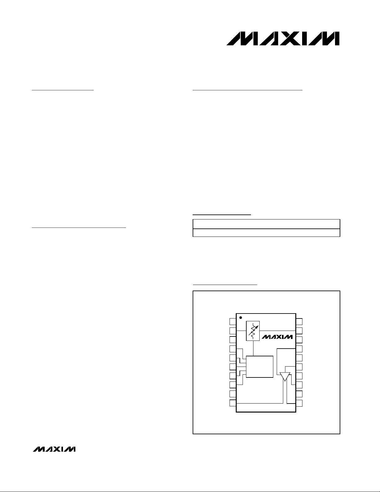
TSSOP
MAX2055
TOP VIEW
19-2799; Rev 0; 4/03
For pricing, delivery, and ordering information, please contact Maxim/Dallas Direct! at
1-888-629-4642, or visit Maxim’s website at www.maxim-ic.com.
*EP = Exposed paddle.
Pin Configuration/
Functional Diagram
PART TEMP RANGE PIN-PACKAGE
MAX2055EUP-T -40°C to +85°C 20 TSSOP-EP*
Page 2
MAX2055
Digitally Controlled, Variable-Gain, Differential
ADC Driver/Amplifier
2 _______________________________________________________________________________________
ABSOLUTE MAXIMUM RATINGS
DC ELECTRICAL CHARACTERISTICS
(Circuit of Figure 1; VCC= +4.75V to +5.25V, GND = 0V. No input signals applied, and input and output ports are terminated with
50Ω. R1 = 1.13kΩ, T
A
= -40°C to +85°C. Typical values are at VCC= +5V and TA= +25°C, unless otherwise noted.) (Notes 1, 2)
Stresses beyond those listed under “Absolute Maximum Ratings” may cause permanent damage to the device. These are stress ratings only, and functional
operation of the device at these or any other conditions beyond those indicated in the operational sections of the specifications is not implied. Exposure to
absolute maximum rating conditions for extended periods may affect device reliability.
All Pins to GND. .....................................-0.3V to +(VCC+ 0.25V)
Input Signal (RF_IN)............................…………………….20dBm
Output Power (RF_OUT) ...................................................24dBm
Continuous Power Dissipation (T
A
= +70°C)
20-Pin TSSOP (derate 21.7mW/°C above +70°C) ...........2.1W
Operating Temperature Range ...........................-40°C to +85°C
Junction Temperature......................................................+150°C
Storage Temperature Range .............................-65°C to +165°C
Lead Temperature (soldering, 10s) .................................+300°C
AC ELECTRICAL CHARACTERISTICS
(Circuit of Figure 1; VCC= +4.75V to +5.25V, GND = 0V, max gain (B0 = B1 = B2 = B3 = B4 = 0), R1= 1.13kΩ, P
OUT
= 5dBm,
f
IN
= 70MHz, 50Ω system impedance. Typical values are at VCC= +5V and TA= +25°C, unless otherwise noted.) (Notes 1, 2)
SUPPLY
Supply Voltage V
Supply Current I
I
SET
CONTROL INPUTS
Control Bits Parallel 5 Bits
Input Logic High 2V
Input Logic Low 0.6 V
Input Leakage Current -1.2 +1.2 µA
PARAMETER SYMBOL CONDITIONS MIN TYP MAX UNITS
Current I
CC
CC
SET
4.75 5.0 5.25 V
240 290 mA
1.1 mA
Frequency Range f
Gain G 19.9 dB
Amplitude Unbalance (Note 3) 0.06 dB
Phase Unbalance (Note 3) 0.7 D eg r ees
Minimum Reverse Isolation 29 dB
Noise Figure NF 5.8 dB
Output 1dB Compression Point P
2nd-Order Output Intercept Point OIP2
3rd-Order Output Intercept Point OIP3 All gain conditions, 5dBm/tone at RF_OUT 40 dBm
2nd Harmonic 2f
3rd Harmonic 3f
RF Gain-Control Range 23 dB
Gain-Control Resolution 1dB
Attenuation Absolute Accuracy Compared to the ideal expected attenuation ±0.2 dB
Attenuation Relative Accuracy Between adjacent states
Gain Drift Over Temperature TA = -40°C to +85°C ±0.3 dB
PARAMETER SYMBOL CONDITIONS MIN TYP MAX UNITS
R
1dB
IN
IN
f
+ f2, f1 = 70MHz, f2 = 71MHz, 5dBm/tone
1
at RF_OUT
30 300 MHz
25.7 dBm
75 dBm
-76 dBc
-69 dBc
+0.05/
-0.2
dB
Page 3
MAX2055
Digitally Controlled, Variable-Gain, Differential
ADC Driver/Amplifier
_______________________________________________________________________________________ 3
Note 1: Guaranteed by design and characterization.
Note 2: All limits reflect losses of external components. Output measurements are taken at RF_OUT using the application circuit
shown in Figure 1.
Note 3: The amplitude and phase unbalance are tested with 50Ω resistors connected from OUT+/OUT- to GND.
AC ELECTRICAL CHARACTERISTICS (continued)
(Circuit of Figure 1; VCC= +4.75V to +5.25V, GND = 0V, max gain (B0 = B1 = B2 = B3 = B4 = 0), R1= 1.13kΩ, P
OUT
= 5dBm,
f
IN
= 70MHz, 50Ω system impedance. Typical values are at VCC= +5V and TA= +25°C, unless otherwise noted.) (Notes 1, 2)
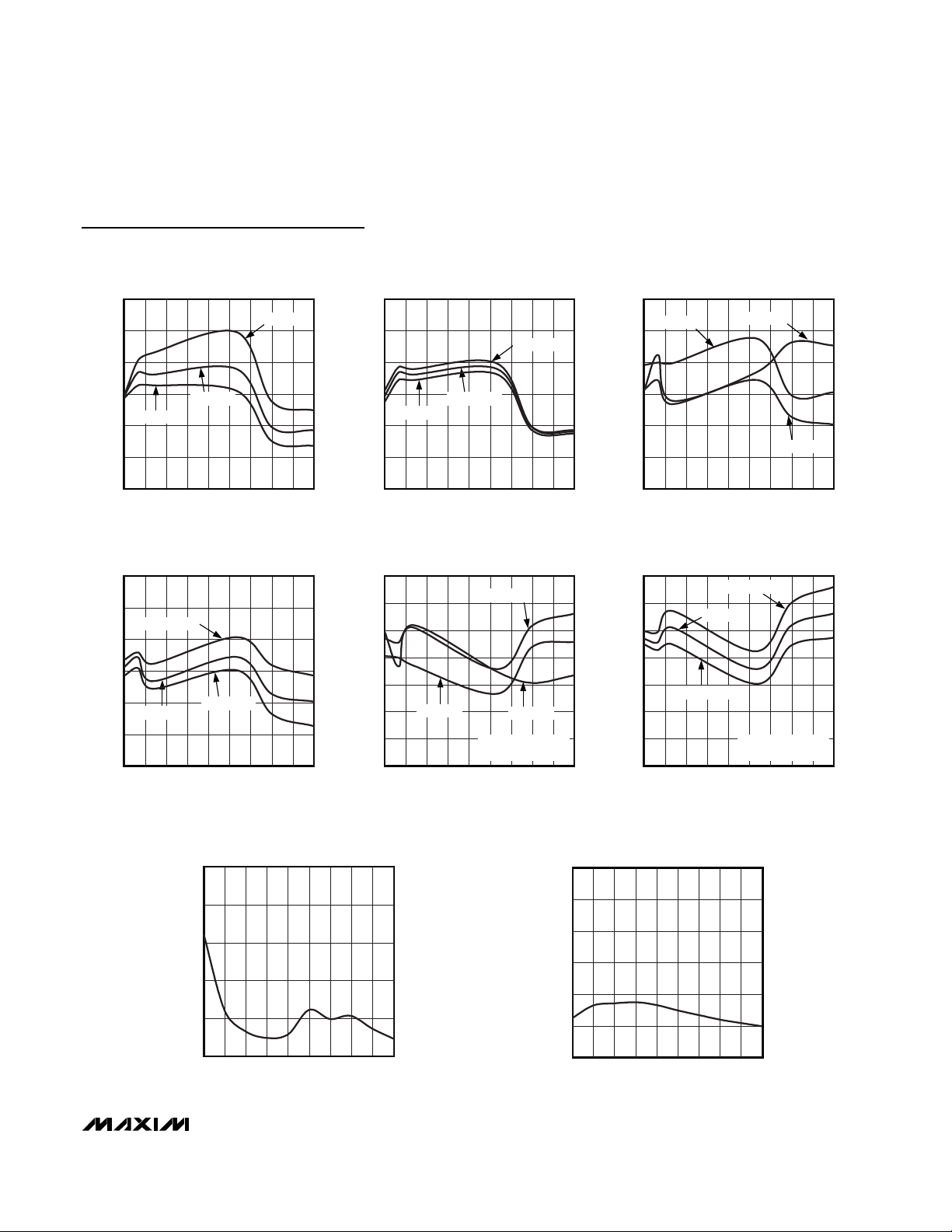
Typical Operating Characteristics
(Circuit of Figure 1, VCC= 5.0V, R1= 1.13kΩ, max gain (B0 = B1 = B2 = B3 = B4 = 0), P
OUT
= 5dBm, TA= +25°C, unless other-
wise noted.)
SUPPLY CURRENT vs. TEMPERATURE
MAX2055 toc01
TEMPERATURE (°C)
SUPPLY CURRENT (mA)
603510-15
220
230
240
250
260
270
210
-40 85
VCC = 5.25V
VCC = 5.0V
VCC = 4.75V
INPUT RETURN LOSS vs. RF FREQUENCY
(ALL STATES)
MAX2055 toc02
FREQUENCY (MHz)
INPUT RETURN LOSS (dB)
27024060 90 120 180150 210
35
30
25
20
15
10
5
0
40
30 300
OUTPUT RETURN LOSS vs. RF FREQUENCY
(ALL STATES)
MAX2055 toc03
FREQUENCY (MHz)
OUTPUT RETURN LOSS (dB)
27024060 90 120 180150 210
35
30
25
20
15
10
5
0
40
30 300
GAIN vs. RF FREQUENCY (ALL STATES)
MAX2055 toc04
FREQUENCY (MHz)
GAIN (dB)
27024060 90 120 180150 210
-5
0
5
10
15
20
25
-10
30 300
GAIN vs. RF FREQUENCY
MAX2055 toc05
FREQUENCY (MHz)
GAIN (dB)
27024060 90 120 180150 210
12
14
16
18
20
22
24
10
30 300
TA = +85°C
TA = +25°C
TA = -40°C
GAIN vs. RF FREQUENCY
MAX2055 toc06
FREQUENCY (MHz)
GAIN (dB)
27024060 90 120 180150 210
12
14
16
18
20
22
24
10
30 300
VCC = 5.25V
VCC = 5.0V
VCC = 4.75V
Gain Flatness Over 50MHz
Bandwidth
PARAMETER SYMBOL CONDITIONS MIN TYP MAX UNITS
Peak-to-peak for all settings 0.5 dB
Attenuator Switching Time 50% control to 90% RF 40 ns
Input Return Loss fR = 30MHz to 300MHz, all gain conditions 15 dB
Output Return Loss
fR = 30MHz to 250MHz, all gain conditions 15
= 250MHz to 300MHz, all gain conditions 12
f
R
dB
Page 4
MAX2055
Digitally Controlled, Variable-Gain, Differential
ADC Driver/Amplifier
4 _______________________________________________________________________________________
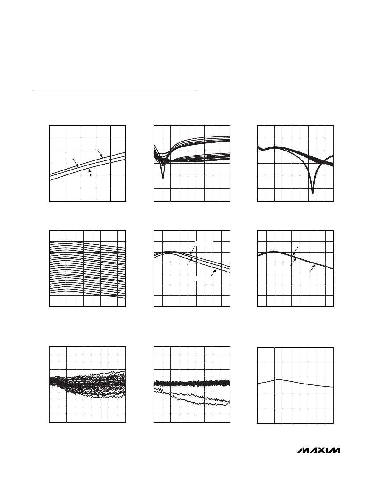
Typical Operating Characteristics (continued)
(Circuit of Figure 1, VCC= 5.0V, R1= 1.13kΩ, max gain (B0 = B1 = B2 = B3 = B4 = 0), P
OUT
= 5dBm, TA= +25°C, unless other-
wise noted.)
ATTENUATION ABSOLUTE ACCURACY
(ALL STATES)
1.0
0.8
0.6
0.4
0.2
0
-0.2
-0.4
ABSOLUTE ACCURACY (dB)
-0.6
-0.8
-1.0
30 300
FREQUENCY (MHz)
MAX2055 toc07
27024060 90 120 180150 210
ATTENUATION RELATIVE ACCURACY
(ALL STATES)
1.0
0.8
0.6
0.4
0.2
0
-0.2
-0.4
RELATIVE ACCURACY (dB)
-0.6
-0.8
-1.0
30 300
FREQUENCY (MHz)
27024060 90 120 180150 210
MAX2055 toc08
REVERSE ISOLATION vs. RF FREQUENCY
40
36
32
28
REVERSE ISOLATION (dB)
24
20
30 300
FREQUENCY (MHz)
MAX2055 toc09
27024060 90 120 180150 210
NOISE FIGURE vs. FREQUENCY
8.0
7.5
7.0
6.5
6.0
5.5
NOISE FIGURE (dB)
5.0
4.5
4.0
TA = +85°C
TA = -40°C
30 300
FREQUENCY (MHz)
OUTPUT IP3 vs. FREQUENCY
44
42
40
38
TA = +85°C
36
OIP3 (dBm)
34
32
30
30 300
TA = +25°C
P
= P
RF1
AT OUTPUT, ∆f = 1MHz
FREQUENCY (MHz)
TA = +25°C
TA = -40°C
= 5dBm
RF2
OUTPUT P-1dB vs. FREQUENCY
27
26
MAX2055 toc10
25
24
23
OUTPUT P-1dB (dBm)
22
27024060 90 120 180150 210
21
30 300
TA = +85°C
TA = -40°C
FREQUENCY (MHz)
TA = +25°C
MAX2055 toc11
OUTPUT P-1dB (dBm)
27024060 90 120 180150 210
OUTPUT IP3 vs. FREQUENCY
44
42
MAX2055 toc13
40
38
36
OIP3 (dBm)
34
32
27024060 90 120 180150 210
30
VCC = +5.25V
VCC = +5V
VCC = +4.75V
P
= P
= 5dBm
RF1
RF2
AT OUTPUT, ∆f = 1MHz
30 300
FREQUENCY (MHz)
27024060 90 120 180150 210
MAX2055 toc14
IIP3 (dBm)
OUTPUT P-1dB vs. FREQUENCY
27
26
25
24
VCC = +5V
23
22
21
30 300
VCC = +5.25V
VCC = +4.75V
FREQUENCY (MHz)
MAX2055 toc12
27024060 90 120 180150 210
INPUT IP3 vs. ATTENUATION STATE
55
50
45
40
35
30
25
20
15
024
P
= P
RF1
AT OUTPUT, ∆f = 1MHz,
= 70MHz
f
IN
ATTENUATION STATE
RF2
= 5dBm
MAX2055 toc15
20164 8 12
Page 5
MAX2055
Digitally Controlled, Variable-Gain, Differential
ADC Driver/Amplifier
_______________________________________________________________________________________ 5
Typical Operating Characteristics (continued)
(Circuit of Figure 1, VCC= 5.0V, R1= 1.13kΩ, max gain (B0 = B1 = B2 = B3 = B4 = 0), P
OUT
= 5dBm, TA= +25°C, unless other-
wise noted.)
HARMONIC (dBc)
HARMONIC (dBc)
3RD HARMONIC vs. FREQUENCY
-55
-60
-65
-70
TA = +85°C
-75
-80
-85
30 300
TA = +25°C
FREQUENCY (MHz)
TA = -40°C
2ND HARMONIC vs. FREQUENCY
-60
-65
VCC = +5.25V
-70
-75
-80
VCC = +5V
-85
-90
30 300
VCC = +4.75V
FREQUENCY (MHz)
3RD HARMONIC vs. FREQUENCY
-55
-60
MAX2055 toc16
-65
-70
VCC = +4.75V
HARMONIC (dBc)
-75
-80
27024060 90 120 180150 210
-85
30 300
VCC = +5V
FREQUENCY (MHz)
VCC = +5.25V
MAX2055 toc17
27024060 90 120 180150 210
OUTPUT IP2 vs. FREQUENCY (f1 + f2)
85
80
MAX2055 toc19
75
70
65
OIP2 (dBm)
60
55
27024060 90 120 180150 210
50
TA = -40°C
30 300
TA = +25°C
P
= P
RF1
AT OUTPUT, ∆f = 1MHz
FREQUENCY (MHz)
TA = +85°C
= 5dBm
RF2
MAX2055 toc20
27024060 90 120 180150 210
2ND HARMONIC vs. FREQUENCY
-60
TA = -40°C
-65
-70
-75
HARMONIC (dBc)
-80
-85
-90
30 300
TA = +85°C
FREQUENCY (MHz)
OUTPUT IP2 vs. FREQUENCY (f1 + f2)
85
80
75
70
65
OIP2 (dBm)
60
55
50
30 300
VCC = +5.0
VCC = +5.25V
FREQUENCY (MHz)
VCC = +4.75V
P
= P
RF1
RF2
AT OUTPUT, ∆f = 1MHz
MAX2055 toc18
TA = +25°C
27024060 90 120 180150 210
MAX2055 toc21
= 5dBm
27024060 90 120 180150 210
OUTPUT-PORT AMPLITUDE UNBALANCE
vs. FREQUENCY
0.25
0.20
0.15
0.10
AMPLITUDE UNBALANCE (dB)
0.05
0
30 300
FREQUENCY (MHz)
MAX2055 toc22
27024060 90 120 180150 210
OUTPUT-PORT PHASE UNBALANCE
vs. FREQUENCY
3.0
2.5
2.0
1.5
1.0
PHASE UNBALANCE (DEGREES)
0.5
0
30 300
FREQUENCY (MHz)
MAX2055 toc23
27024060 90 120 180150 210
Page 6
SUPPLY CURRENT vs. TEMPERATURE
MAX2055 toc24
TEMPERATURE (°C)
SUPPLY CURRENT (mA)
603510-15
220
230
240
250
260
270
210
-40 85
VCC = 5.25V
VCC = 5.0V
VCC = 4.75V
INPUT RETURN LOSS vs. RF FREQUENCY
(ALL STATES)
MAX2055 toc25
FREQUENCY (MHz)
INPUT RETURN LOSS (dB)
27024060 90 120 180150 210
50
40
30
20
10
0
60
30 300
OUTPUT RETURN LOSS vs. FREQUENCY
(ALL STATES)
MAX2055 toc26
FREQUENCY (MHz)
OUTPUT RETURN LOSS (dB)
27024060 90 120 180150 210
50
40
30
20
10
0
60
30 300
GAIN vs. RF FREQUENCY (ALL STATES)
MAX2055 toc27
FREQUENCY (MHz)
GAIN (dB)
27024060 90 120 180150 210
-5
0
5
10
15
20
25
-10
30 300
GAIN vs. RF FREQUENCY
MAX2055 toc28
FREQUENCY (MHz)
GAIN (dB)
27024060 90 120 180150 210
12
14
16
18
20
22
24
10
30 300
TA = +85°C
TA = +25°C
TA = -40°C
GAIN vs. RF FREQUENCY
MAX2055 toc29
FREQUENCY (MHz)
GAIN (dB)
27024060 90 120 180150 210
12
14
16
18
20
22
24
10
30 300
VCC = 5.25V
VCC = 5.0V
VCC = 4.75V
ATTENUATION ABSOLUTE ACCURACY
(ALL STATES)
MAX2055 toc30
FREQUENCY (MHz)
ABSOLUTE ACCURACY (dB)
27024060 90 120 180150 210
-0.8
-0.6
-0.4
-0.2
0
0.2
0.4
0.6
0.8
1.0
-1.0
30 300
ATTENUATION RELATIVE ACCURACY
(ALL STATES)
MAX2055 toc31
FREQUENCY (MHz)
RELATIVE ACCURACY (dB)
27024060 90 120 180150 210
-0.8
-0.6
-0.4
-0.2
0
0.2
0.4
0.6
0.8
1.0
-1.0
30 300
REVERSE ISOLATION vs. RF FREQUENCY
MAX2055 toc32
FREQUENCY (MHz)
REVERSE ISOLATION (dB)
27024060 90 120 180150 210
24
28
32
36
40
20
30 300
MAX2055
Digitally Controlled, Variable-Gain, Differential
ADC Driver/Amplifier
6 _______________________________________________________________________________________
Typical Operating Characteristics
(Circuit of Figure 2, VCC= 5.0V, R1= 909Ω, max gain, (B0 = B1 = B2 = B3 = B4 = 0), P
OUT
= 5dBm, TA= +25°C, unless otherwise
noted.)
Page 7
MAX2055
Digitally Controlled, Variable-Gain, Differential
ADC Driver/Amplifier
_______________________________________________________________________________________ 7
Typical Operating Characteristics (continued)
(Circuit of Figure 2, VCC= 5.0V, R1= 909Ω, max gain, (B0 = B1 = B2 = B3 = B4 = 0), P
OUT
= 5dBm, TA= +25°C, unless otherwise
noted.)
NOISE FIGURE vs. FREQUENCY
MAX2055 toc33
FREQUENCY (MHz)
NOISE FIGURE (dB)
27024060 90 120 180150 210
4.5
5.0
5.5
6.0
6.5
7.0
7.5
8.0
4.0
30 300
TA = +85°C
TA = -40°C
TA = +25°C
OUTPUT P-1dB vs. FREQUENCY
MAX2055 toc34
FREQUENCY (MHz)
OUTPUT P-1dB (dBm)
27024060 90 120 180150 210
22
23
24
25
26
27
21
30 300
TA = +85°C
TA = -40°C
T
A
= +25°C
OUTPUT P-1dB vs. FREQUENCY
MAX2055 toc35
FREQUENCY (MHz)
OUTPUT P-1dB (dBm)
27024060 90 120 180150 210
22
23
24
25
26
27
21
30 300
VCC = +4.75V
VCC = +5V
VCC = +5.25V
OUTPUT IP3 vs. FREQUENCY
MAX2055 toc36
FREQUENCY (MHz)
OIP3 (dBm)
27024060 90 120 180150 210
32
34
36
38
42
40
44
30
30 300
TA = +85°C
TA = -40°C
TA = +25°C
P
RF1
= P
RF2
= 5dBm
AT OUTPUT, ∆f = 1MHz
OUTPUT IP3 vs. FREQUENCY
MAX2055 toc37
FREQUENCY (MHz)
OIP3 (dBm)
27024060 90 120 180150 210
32
34
36
38
42
40
44
30
30 300
VCC = +5.25V
VCC = +4.75V
VCC = +5V
P
RF1
= P
RF2
= 5dBm
AT OUTPUT, ∆f = 1MHz
INPUT IP3 vs. ATTENUATION STATE
MAX2055 toc38
ATTENUATION STATE
IIP3 (dBm)
20164 8 12
20
25
30
35
40
45
50
55
15
024
P
RF1
= P
RF2
= 5dBm
AT OUTPUT, ∆f = 1MHz,
f
IN
= 70MHz
3RD HARMONIC vs. FREQUENCY
MAX2055 toc39
FREQUENCY (MHz)
HARMONIC (dBc)
27024060 90 120 180150 210
-80
-75
-70
-65
-60
-55
-85
30 300
TA = +85°C
TA = -40°C
TA = +25°C
3RD HARMONIC vs. FREQUENCY
MAX2055 toc40
FREQUENCY (MHz)
HARMONIC (dBc)
27024060 90 120 180150 210
-80
-75
-70
-65
-60
-55
-85
30 300
VCC = +4.75V
VCC = +5V
VCC = +5.25V
2ND HARMONIC vs. FREQUENCY
MAX2055 toc41
FREQUENCY (MHz)
HARMONIC (dBc)
27024060 90 120 180150 210
-80
-75
-70
-65
-60
-55
-50
-85
-90
30 300
TA = +85°C
TA = -40°C
TA = +25°C
Page 8
MAX2055
Digitally Controlled, Variable-Gain, Differential
ADC Driver/Amplifier
8 _______________________________________________________________________________________
Typical Operating Characteristics (continued)
(Circuit of Figure 2, VCC= 5.0V, R1= 909Ω, max gain, (B0 = B1 = B2 = B3 = B4 = 0), P
OUT
= 5dBm, TA= +25°C, unless otherwise
noted.)
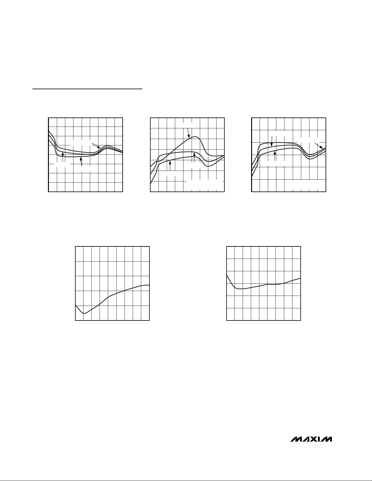
HARMONIC (dBc)
2ND HARMONIC vs. FREQUENCY
-50
-55
-60
VCC = +5V
VCC = +5.25V
VCC = +4.75V
FREQUENCY (MHz)
-65
-70
-75
-80
-85
-90
30 300
OUTPUT IP2 vs. FREQUENCY (f1 + f2)
85
TA = -40°C
FREQUENCY (MHz)
TA = +85°C
TA = +25°C
P
RF1
AT OUTPUT, ∆f = 1MHz
= P
RF2
= 5dBm
80
MAX2055 toc42
75
70
65
OIP2 (dBm)
60
55
27024060 90 120 180150 210
50
30 300
27024060 90 120 180150 210
OUTPUT IP2 vs. FREQUENCY (f1 + f2)
80
75
MAX2055 toc43
70
65
OIP2 (dBm)
60
55
50
VCC = +5.0V
VCC = +5.25V
P
RF1
AT OUTPUT, ∆f = 1MHz
30 300
FREQUENCY (MHz)
VCC = +4.75V
= P
RF2
MAX2055 toc44
= 5dBm
27024060 90 120 180150 210
OUTPUT-PORT AMPLITUDE UNBALANCE
vs. FREQUENCY
0.25
0.20
0.15
0.10
AMPLITUDE UNBALANCE (dB)
0.05
0
30 300
FREQUENCY (MHz)
OUTPUT-PORT PHASE UNBALANCE
vs. FREQUENCY
3.0
MAX2055 toc45
27024060 90 120 180150 210
2.5
2.0
1.5
1.0
PHASE UNBALANCE (DEGREES)
0.5
0
30 300
FREQUENCY (MHz)
MAX2055 toc46
27024060 90 120 180150 210
Page 9

MAX2055
Digitally Controlled, Variable-Gain, Differential
ADC Driver/Amplifier
_______________________________________________________________________________________ 9
Pin Description
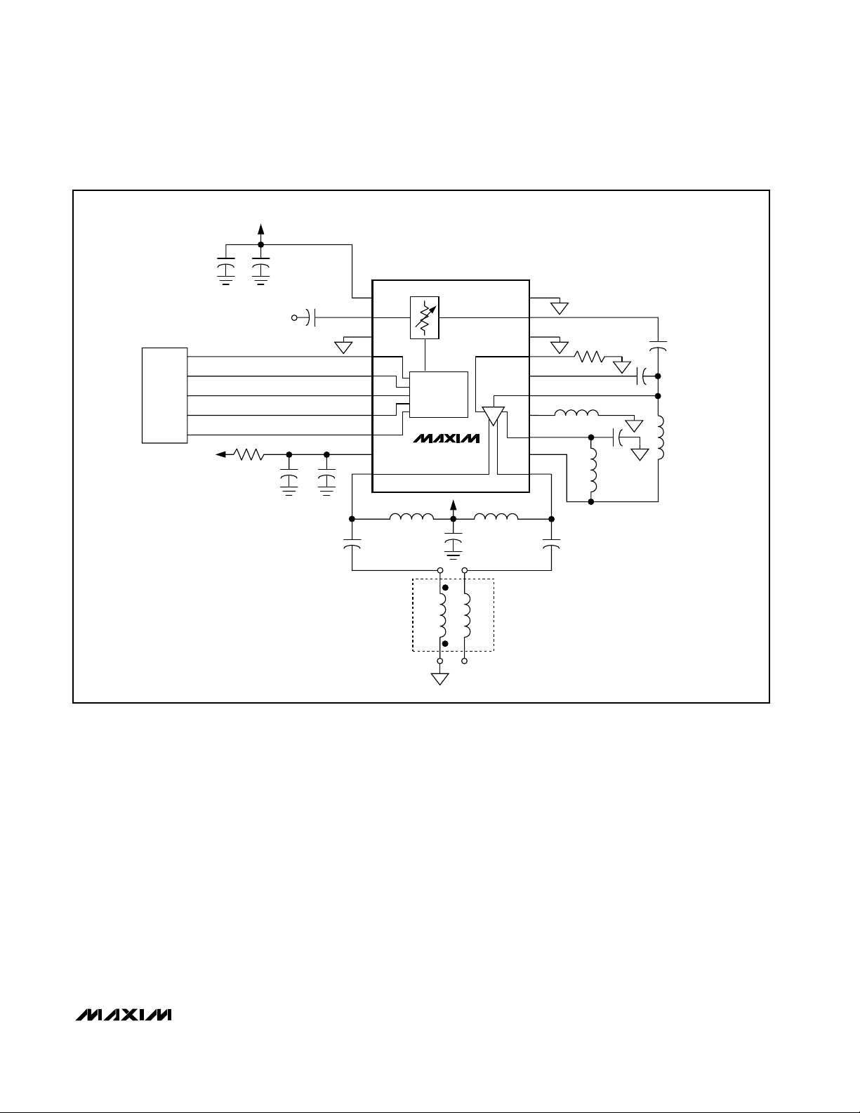
Table 1. Suggested Components of
Circuit of Figure 1
Table 2. Suggested Components of
Circuit of Figure 2
PIN NAME FUNCTION
1, 9 V
2 RF_IN
3, 18, 20, EP GND
4–8B4–B0 Attenuation Control Bits. Digital input for attenuation control. See Table 3 for attenuation setting.
10 RF_OUT-
11 RF_OUT+
12 I
13 C
14 L
15 AMP
16 C
17 I
19 ATTN
CC
BIAS
BP
E
C
SET
Power Supply. Bypass to GND with capacitors as close to the pin as possible as shown in the typical
application circuits (Figures 1 and 2).
Signal Input. Internally matched to 50Ω over the operating frequency. See the typical application
circuit for recommended component values.
Ground. Use low-inductance layout techniques on the PC board. Solder the exposed paddle to the
board ground plane.
Inverted Differential Signal Output. Requires an external pullup choke inductor (120mA typical
current) to V
Noninverted Differential Signal Output. Requires an external pullup choke inductor (120mA typical
current) to V
Amplifier Bias Input. See Figures 1 and 2 for detailed connection.
Bypass Capacitor. See Figures 1 and 2 for detailed connection.
Amplifier DC Ground. Requires choke inductor that can handle supply current. DC resistance of
inductor should be less than 0.2Ω.
Amplifier Input. Requires DC-coupling to allow biasing.
IN
Compensation Capacitor. Requires connection to AMPIN (pin 15) for stability.
Connect R1 from I
Attenuator Output. Requires external DC-blocking capacitor.
OUT
along with a DC-blocking capacitor; see Figures 1 and 2.
CC
along with a DC-blocking capacitor; see Figures 1 and 2.
CC
to GND (see Table 1 or Table 2 for values).
SET
C1, C3–C6, C8, C9, C10, C12 1nF 0603
C2, C11 100pF 0603
L1, L3 330nH 0603
L2 100nH 0603
L4, L5 680nH 1008
R1 1.13kΩ 0603
R7 10Ω 0603
T1, T2 1:1 —
COMPONENT VALUE SIZE
C1, C3, C4, C5, C7–C10, C12 1nF 0603
C2, C11 100pF 0603
L1, L2, L3 330nH 0603
L4, L5 680nH 1008
R1 909Ω 0603
R7 10Ω 0603
T2 1:1 —
COMPONENT VALUE SIZE
Page 10

MAX2055
Detailed Description
The MAX2055 is a high-dynamic-range, digitally controlled, variable-gain differential ADC driver/amplifier
(DVGA) for use in applications from 30MHz to 300MHz.
The amplifier is designed for 50Ω single-ended input
and 50Ω differential output systems.
The MAX2055 integrates a digital attenuator with a
23dB selectable attenuation range and a high-linearity,
single-ended-to-differential output amplifier. The attenuator is digitally controlled through five logic lines:
B0–B4. The on-chip attenuator provides up to 23dB of
attenuation with ±0.2dB accuracy. The single-ended
input to differential output amplifier utilizes negative
feedback to achieve high gain and linearity over a wide
bandwidth.
Applications Information
Digitally Controlled Attenuator
The digital attenuator is controlled through five logic
lines: B0, B1, B2, B3, and B4. Table 3 lists the attenuation settings. The input and output of this attenuator
require external DC blocking capacitors. The attenuator’s insertion loss is approximately 2dB, when the control bits are set to 0dB (B0 = B1 = B2 = B3 = B4 = 0).
Single-Ended-to-Differential Amplifier
The MAX2055 integrates a single-ended-to-differential
amplifier with a nominal gain of 22dB in a negative
Digitally Controlled, Variable-Gain, Differential
ADC Driver/Amplifier
10 ______________________________________________________________________________________
Figure 1. Typical Application Circuit
V
CC
C
C
3
CONTROL
INPUTS
V
CC
2
1
V
CC
RF_IN
RF_IN
C
1
R
7
C
C
12
11
2
3
GND
4
B4
5
B3
B2
B1
B0
V
CC
RF_OUT-
ATTENUATION
LOGIC
CONTROL
MAX2055
L
5
1
V
CC
C
10
6
7
8
9
10
C
8
GND
ATTN
GND
AMP
I
RF_OUT+
L
4
OUT
I
C
BIAS
20
19
18
SET
17
16
C
C
15
IN
14
L
E
13
BP
12
11
R
1
L
2
L
3
C
9
C4
C
5
C
6
T
1
1
L
1
T
2
RF_OUT
Page 11
feedback topology. This amplifier is optimized for a frequency range of operation from 30MHz to 300MHz with
a high-output third-order intercept point (OIP3). The
bias current is chosen to optimize the IP3 of the amplifier. When R1is 1.13kΩ (909Ω if using the circuit of
Figure 2), the current consumption is 240mA while
exhibiting a 40dBm typical output IP3 at 70MHz. The
common-mode inductor, L2, provides a high commonmode rejection with excellent amplitude and phase balance at the output. L2must handle the supply current
and have DC resistance less than 0.2Ω.
Choke Inductor
The single-ended amplifier input and differential output
ports require external choke inductors. At the input,
connect a 330nH bias inductor from AMPIN(pin 15) to
I
BIAS
(pin 12). Connect 680nH choke inductors from
RF_OUT+ (pin 11) and RF_OUT- (pin 10) to VCC. These
connections provide bias current to the amplifier.
Layout Considerations
A properly designed PC board is an essential part of
any RF/microwave circuit. Keep RF signal lines as short
as possible to reduce losses, radiation, and inductance. For best performance, route the ground-pin
traces directly to the exposed pad underneath the
MAX2055
Digitally Controlled, Variable-Gain, Differential
ADC Driver/Amplifier
______________________________________________________________________________________ 11
Figure 2. Low-Cost Application Circuit
CONTROL
INPUTS
V
CC
C
C
3
2
1
V
CC
RF_IN
RF_IN
C
1
R
V
CC
7
C
C
12
11
2
3
GND
4
B4
5
B3
B2
B1
B0
V
CC
RF_OUT-
ATTENUATION
LOGIC
CONTROL
MAX2055
L
5
1
V
CC
C
10
6
7
8
9
10
C
8
GND
ATTN
GND
AMP
I
RF_OUT+
L
4
OUT
I
C
BIAS
20
19
18
SET
17
16
C
C
15
IN
14
L
E
13
BP
12
11
R
1
L
2
C
7
L
3
C
9
C
4
C
5
L
1
T
2
RF_OUT
Page 12

MAX2055
package. This pad should be connected to the ground
plane of the board by using multiple vias under the
device to provide the best RF/thermal conduction path.
Solder the exposed pad on the bottom of the device
package to a PC board exposed pad.
The MAX2055 Evaluation Kit can be used as a reference for board layout. Gerber files are available upon
request at www.maxim-ic.com.
Power-Supply Bypassing
Proper voltage-supply bypassing is essential for highfrequency circuit stability. Bypass each VCCpin with a
1000pF and 100pF capacitor. Connect the 100pF
capacitor as close to the device as possible. Resistor
R7 helps reduce switching transients. If switching transients are not a concern, R7 is not required. Therefore,
connect pin 9 directly to VCC.
Exposed Paddle RF Thermal
Considerations
The EP of the MAX2055’s 20-pin TSSOP-EP package
provides a low thermal-resistance path to the die. It is
important that the PC board on which the IC is mounted
be designed to conduct heat from this contact. In addition, the EP provides a low-inductance RF ground path
for the device.
It is recommended that the EP be soldered to a ground
plane on the PC board, either directly or through an
array of plated via holes.
Soldering the pad to ground is also critical for efficient
heat transfer. Use a solid ground plane wherever
possible.
Digitally Controlled, Variable-Gain, Differential
ADC Driver/Amplifier
12 ______________________________________________________________________________________
Table 3. Attenuation Setting vs. GainControl Bits
*Enabling B4 disables B3 and the minimum attenuation is
16dB.
Chip Information
TRANSISTOR COUNT: 325
PROCESS: BiCMOS
ATTENUATION B4 B3* B2 B1 B0
0 00000
1 00001
2 00010
3 00011
4 00100
5 00101
6 00110
7 00111
8 01000
9 01001
10 01010
11 01011
12 01100
13 01101
14 01110
15 01111
16 1 X 0 0 0
17 1 X 0 0 1
18 1 X 0 1 0
19 1 X 0 1 1
20 1 X 1 0 0
21 1 X 1 0 1
22 1 X 1 1 0
23 1 X 1 1 1
Page 13

MAX2055
Digitally Controlled, Variable-Gain, Differential
ADC Driver/Amplifier
Maxim cannot assume responsibility for use of any circuitry other than circuitry entirely embodied in a Maxim product. No circuit patent licenses are
implied. Maxim reserves the right to change the circuitry and specifications without notice at any time.
Maxim Integrated Products, 120 San Gabriel Drive, Sunnyvale, CA 94086 408-737-7600 ____________________ 13
© 2003 Maxim Integrated Products Printed USA is a registered trademark of Maxim Integrated Products.
Package Information
(The package drawing(s) in this data sheet may not reflect the most current specifications. For the latest package outline information,
go to www.maxim-ic.com/packages
.)
TSSOP4.40mm.EPS
 Loading...