

Page 1
General Description
The MAX2051 high-linearity, up/downconversion mixer
provides +35dBm input IP3, 7.8dB noise figure (NF), and
7.4dB conversion loss for 850MHz to 1550MHz wireless
infrastructure and multicarrier cable head-end downstream video, video-on-demand (VOD), and cable
modem termination systems (CMTS) applications. The
MAX2051 also provides excellent suppression of spurious intermodulation products (> 77dBc at an RF level of
-14dBm), making it an ideal downconverter for DOCSIS
®
3.0 and Euro DOCSIS cable head-end systems. With an
LO circuit tuned to support frequencies ranging from
1200MHz to 2250MHz, the MAX2051 is ideal for highside LO injection applications over an IF frequency
range of 50MHz to 1000MHz.
In addition to offering excellent linearity and noise performance, the MAX2051 also yields a high level of component integration. The device integrates baluns in the
RF and LO ports, which allow for a single-ended RF
input and a single-ended LO input. The MAX2051
requires a typical LO drive of 0dBm and a supply current guaranteed to below 130mA.
The MAX2051 is available in a compact 5mm x 5mm,
20-pin thin QFN package with an exposed pad.
Electrical performance is guaranteed over the extended
temperature range, from TC= -40°C to +85°C.
Applications
Video-on-Demand and DOCSIS-Compatible
Edge QAM Modulation
Cable Modem Termination Systems
Microwave and Fixed Broadband Wireless
Access
Microwave Links
Military Systems
Predistortion Receivers
Private Mobile Radios
Integrated Digital Enhanced Network (iDEN)
Base Stations
WiMAX™ Base Stations and Customer Premise
Equipment
Wireless Local Loop
Features
♦ 850MHz to 1550MHz RF Frequency Range
♦ 1200MHz to 2250MHz LO Frequency Range
♦ 50MHz to 1000MHz IF Frequency Range
♦ DOCSIS 3.0 and Euro DOCSIS Compatible
♦ 7.4dB Typical Conversion Loss
♦ 7.8dB Typical Noise Figure
♦ +24dBm Typical Input 1dB Compression Point
♦ +35dBm Typical Input IP3
♦ 88dBc Typical 2RF-LO Rejection at P
RF
= -14dBm
♦ Integrated LO Buffer
♦ Integrated RF and LO Baluns for Single-Ended
Inputs
♦ Low LO Drive (0dBm Nominal)
♦ External Current-Setting Resistor Provides Option
for Operating Device in Reduced-Power/
Reduced-Performance Mode
MAX2051
SiGe, High-Linearity, 850MHz to 1550MHz
Up/Downconversion Mixer with LO Buffer
________________________________________________________________
Maxim Integrated Products
1
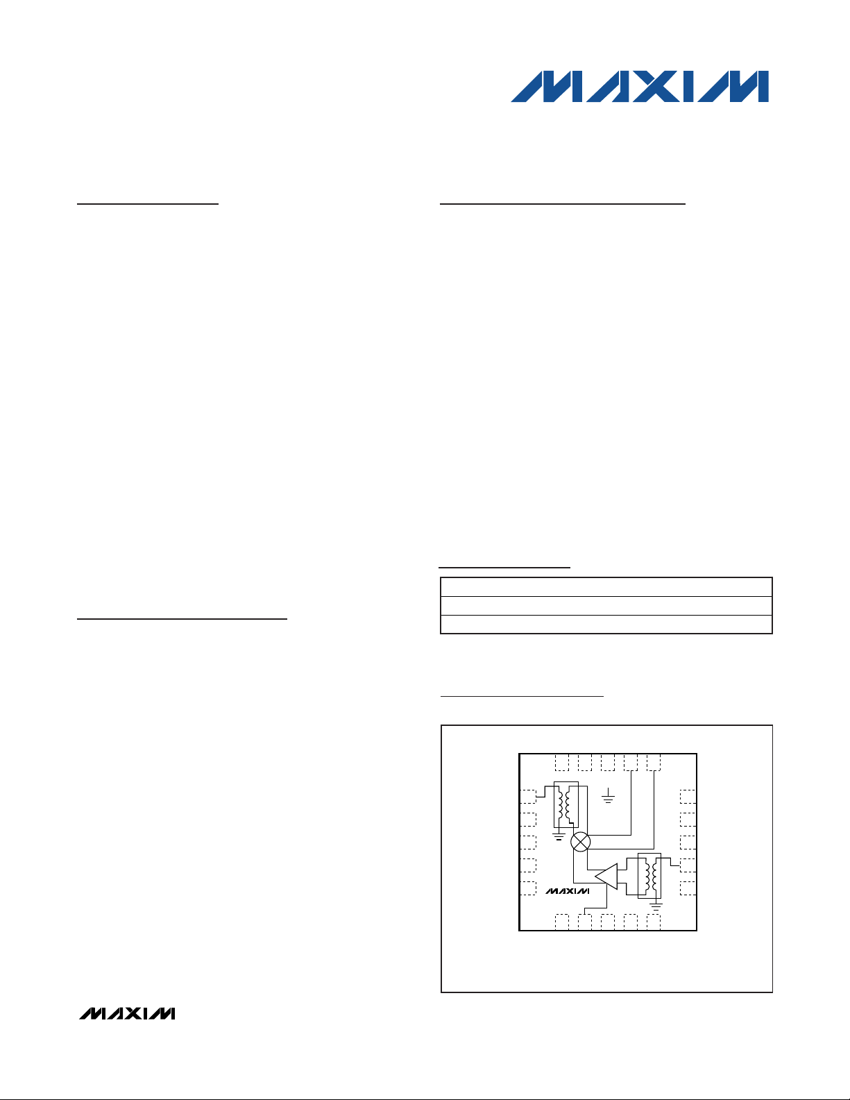
Pin Configuration/
Functional Block Diagram
Ordering Information
19-4582; Rev 0; 4/09
For pricing, delivery, and ordering information, please contact Maxim Direct at 1-888-629-4642,
or visit Maxim’s website at www.maxim-ic.com.
PART TEMP RANGE PIN-PACKAGE
MAX2051ETP+ -40°C to +85°C 20 Thin QFN-EP*
MAX2051ETP+T -40°C to +85°C 20 Thin QFN-EP*
DOCSIS and CableLabs are registered trademarks of Cable
Television Laboratories, Inc. (CableLabs
®
).
iDEN is a registered trademark of Motorola, Inc.
WiMAX is a trademark of WiMAX Forum.
+
Denotes a lead(Pb)-free/RoHS-compliant package.
*
EP = Exposed pad.
T = Tape and reel.
TOP VIEW
+
RF
1
GND
2
3
GND
GND
4
5
GND
*EXPOSED PAD. CONNECT EP TO GND.
GND
GND
20 19 17 16
MAX2051
67
CC
V
LOBIAS
IF-
GND
18
EP*
910
8
CC
V
GND
TQFN
IF+
GND
V
15
CC
14
GND
GND
13
LO
12
GND
11
Page 2
MAX2051
SiGe, High-Linearity, 850MHz to 1550MHz
Up/Downconversion Mixer with LO Buffer
2 _______________________________________________________________________________________
ABSOLUTE MAXIMUM RATINGS
DC ELECTRICAL CHARACTERISTICS
(
Typical Application Circuit
, VCC= +4.75V to +5.25V, no input AC signals. TC= -40°C to +85°C, unless otherwise noted. Typical val-
ues are at V
CC
= +5.0V, TC= +25°C, unless otherwise noted.)
Stresses beyond those listed under “Absolute Maximum Ratings” may cause permanent damage to the device. These are stress ratings only, and functional
operation of the device at these or any other conditions beyond those indicated in the operational sections of the specifications is not implied. Exposure to
absolute maximum rating conditions for extended periods may affect device reliability.
Note 1: Based on junction temperature TJ= TC+ (θJCx VCCx ICC). This formula can be used when the temperature of the exposed
pad is known while the device is soldered down to a PCB. See the
Applications Information
section for details. The junction
temperature must not exceed +150°C.
Note 2: Junction temperature T
J
= TA+ (θJAx VCCx ICC). This formula can be used when the ambient temperature of the PCB is
known. The junction temperature must not exceed +150°C.
Note 3: Package thermal resistances were obtained using the method described in JEDEC specification JESD51-7, using a four-
layer board. For detailed information on package thermal considerations, refer to www.maxim-ic.com/thermal-tutorial
.
Note 4: T
C
is the temperature on the exposed pad of the package. TAis the ambient temperature of the device and PCB.
V
CC
to GND...........................................................-0.3V to +5.5V
RF, LO to GND.........................................................-0.3V to 0.3V
IF+, IF-, LOBIAS to GND ............................-0.3V to (V
CC
+ 0.3V)
RF, LO Input Power ........................................................+20dBm
RF, LO Current (RF and LO is DC shorted to GND
through balun).................................................................50mA
Continuous Power Dissipation (Note 1) ........................2100mW
θ
JA
(Notes 2, 3)..............................................................+33°C/W
θ
JC
(Note 3)........................................................................8°C/W
Operating Case Temperature Range
(Note 4) ...................................................T
C
= -40°C to +85°C
Junction Temperature......................................................+150°C
Storage Temperature Range .............................-65°C to +150°C
Lead Temperature (soldering, 10s) .................................+300°C
RECOMMENDED AC OPERATING CONDITIONS
Supply Voltage V
Supply Current I
PARAMETER SYMBOL CONDITIONS MIN TYP MAX UNITS
CC
CC
Total supply current 105 130 mA
4.75 5 5.25 V
PARAMETER SYMBOL CONDITIONS MIN TYP MAX UNITS
RF Frequency f
LO Frequency f
IF Frequency f
LO Drive Level P
RF
LO
IF
LO
(Notes 5, 6) 850 1550 MHz
(Note 5) 1200 2250 MHz
Meeting RF and LO frequency ranges; IF
matching components affect the IF
frequency range (Note 5)
50 1000 MHz
-3 +9 dBm
Page 3
MAX2051
SiGe, High-Linearity, 850MHz to 1550MHz
Up/Downconversion Mixer with LO Buffer
_______________________________________________________________________________________ 3
AC ELECTRICAL CHARACTERISTICS (DOWNCONVERTER OPERATION)
(
Typical Application Circuit
, VCC= +4.75V to +5.25V, RF and LO ports are driven from 50Ω sources, PLO= -3dBm to +3dBm,
P
RF
= 0dBm, fRF= 1000MHz to 1250MHz, fLO= 1200MHz to 2250MHz, fIF= 50MHz to 1000MHz, fRF< fLO, TC= -40°C to +85°C.
Typical values are at V
CC
= +5.0V, PRF= 0dBm, PLO= 0dBm, fRF=1200MHz, fLO= 1700MHz, fIF= 500MHz, TC=+25°C, unless oth-
erwise noted.) (Note 7)
PARAMETER SYMBOL CONDITIONS MIN TYP MAX UNITS
Conversion Power Loss L
Conversion Power Loss
Temperature Coefficient
Conversion Power Loss Variation
vs. Frequency
Noise Figure NF
Input 1dB Compression Point IP
Third-Order Input Intercept Point IIP3
2RF-LO Spurious Rejection 2 x 1
2LO-2RF Spurious Rejection 2 X 2
TC
ΔL
C
SSB
1dB
fRF = 1200MHz, fLO = 1700MHz,
f
= 500MHz, TC = +25°C (Notes 8, 9)
IF
TC = -40°C to +85°C 0.01 dB/°C
L
fLO = 1200MHz to 2250MHz ± 0.5 dB
C
Single sideband 7.8 dB
V
= + 5.0V ,
C C
f
= 1200M H z,
R F1
= 1201M H z,
f
R F2
P
= 0d Bm tone,
R F
= 1562M H z, P LO = 0d Bm , TC = +25°C,
f
LO
f
= 362M H z ( N otes 8, 9)
IF
Single tone, fRF =1200MHz,
f
= 192.5MHz to 857.5MHz,
IF
= 1392.5MHz to 2057.5MHz,
f
LO
P
= +3dBm, resultant
LO
= 1007.5MHz to 342.5MHz
f
SPUR
(Notes 8, 9, 10)
Single tone, f
= 857.5MHz to 1000MHz,
f
IF
f
= 2057.5MHz to 2200MHz,
LO
= +3dBm, resultant
P
LO
f
= 342.5MHz to 200MHz
SPUR
=1200MHz,
RF
(Notes 8, 9, 10)
Single tone, fRF =1200MHz,
= 97.5MHz to 430MHz,
f
IF
f
= 1297.5MHz to 1630MHz,
LO
= +3dBm, resultant
P
LO
f
= 195MHz to 860MHz
SPUR
(Notes 8, 9, 10)
Single tone, f
f
= 430MHz to 525MHz,
IF
= 1630MHz to 1725MHz,
f
LO
P
= +3dBm, resultant
LO
= 860MHz to 1050MHz
f
SPUR
=1200MHz,
RF
(Notes 8, 9, 10)
PRF =
-14dBm
PRF =
-10dBm
P
=
RF
0dBm
PRF =
-14dBm
PRF =
-10dBm
P
=
RF
0dBm
PRF =
-14dBm
PRF =
-10dBm
=
P
RF
0dBm
PRF =
-14dBm
PRF =
-10dBm
P
=
RF
0dBm
33 35 dBm
73 88
69 84
59 74
74 78
70 74
60 64
68 79
64 75
54 65
71.5 77.4
67.5 73.4
57.5 63.4
7.4 9 dB
24 dBm
dBc
dBc
Page 4
MAX2051
SiGe, High-Linearity, 850MHz to 1550MHz
Up/Downconversion Mixer with LO Buffer
4 _______________________________________________________________________________________
AC ELECTRICAL CHARACTERISTICS (DOWNCONVERTER OPERATION) (continued)
(
Typical Application Circuit
, VCC= +4.75V to +5.25V, RF and LO ports are driven from 50Ω sources, PLO= -3dBm to +3dBm,
P
RF
= 0dBm, fRF= 1000MHz to 1250MHz, fLO= 1200MHz to 2250MHz, fIF= 50MHz to 1000MHz, fRF< fLO, TC= -40°C to +85°C.
Typical values are at V
CC
= +5.0V, PRF= 0dBm, PLO= 0dBm, fRF=1200MHz, fLO= 1700MHz, fIF= 500MHz, TC=+25°C, unless oth-
erwise noted.) (Note 7)
3LO-3RF Spurious Rejection 3 x 3
LO Leakage at RF Port PLO = +3dBm (Notes 6, 8) -33.5 -27.5 dBm
LO Leakage at IF Port PLO = +3dBm (Notes 8, 9) -26.3 -22.9 dBm
RF-to-IF Isolation f
RF Input Impedance Z
RF Input Return Loss
LO Input Impedance Z
LO Input Return Loss
IF Output Impedance Z
PARAMETER SYMBOL CONDITIONS MIN TYP MAX UNITS
Single tone, f
50MHz < f
1250MHz < f
(Notes 8, 9)
= 1200M H z, P
R F
RF
LO on and IF terminated with a matched
impedance
LO
RF and IF terminated with a matched
impedance (Note 11)
Nominal differential impedance at the IC’s
IF
IF outputs
= 1200MHz,
RF
< 1000MHz,
IF
< 2200MHz
LO
L O
= + 3d Bm ( N otes 8, 9) 24 51 dB
PRF =
-14dBm
PRF =
-10dBm
P
= 0dBm 59.5 73
RF
87.5 101
79.5 93
50 Ω
12 dB
50 Ω
11 dB
50 Ω
dBc
IF Output Return Loss
RF ter m i nated i nto 50Ω , LO d r i ven b y 50Ω
sour ce, IF tr ansfor m ed to 50Ω si ng l e- end ed
usi ng exter nal com p onents show n i n the
Typ i cal Ap p l i cati on C i r cui t
15 dB
Page 5
MAX2051
SiGe, High-Linearity, 850MHz to 1550MHz
Up/Downconversion Mixer with LO Buffer
_______________________________________________________________________________________ 5
AC ELECTRICAL CHARACTERISTICS (UPCONVERTER OPERATION)
(
Typical Application Circuit
, RF and LO ports are driven from 50Ω sources, fRF< fLO. Typical values are at VCC= +5.0V, PIF= 0dBm,
P
LO
= 0dBm, fRF= 1250MHz, fLO= 1600MHz fIF= 350MHz, TC=+25°C, unless otherwise noted.) (Note 7)
Note 5: Operation outside this range is possible, but with degraded performance of some parameters. See the
Typical Operating
Characteristics
section.
Note 6: Not production tested.
Note 7: All values reflect losses of external components, including a 0.6dB loss at f
IF
= 350MHz and a 0.8dB loss at
f
IF
= 1000MHz due to the 1:1 transformer. Output measurements were taken at IF outputs of the
Typical Application Circuit
.
Note 8: Guaranteed by design and characterization.
Note 9: 100% production tested for functionality.
Note 10: Additional improvements (of up to 4dB to 6dB) in spurious responses can be made by increasing the LO drive to +6dBm.
Note 11: The LO return loss can be improved by tuning C9 to offset any parasitics within the specific application circuit. Typical
range of C9 is 10pF to 50pF.
Conversion Power Loss L
Third-Order Input Intercept
Point
LO-2IF Spurious Rejection 61 dBc
LO+2IF Spurious Rejection 63.3 dBc
LO-3IF Spurious Rejection 78 dBc
LO+3IF Spurious Rejection 79 dBc
LO Leakage at RF Port PLO = +3dBm -35.7 dBm
IF Leakage at RF Port -52 dBm
RF Return Loss 12.3 dB
IF Input Return Loss fLO = 1200MHz 18 dB
PARAMETER SYMBOL CONDITIONS MIN TYP MAX UNITS
7.5 dB
C
IIP3 f
= 350M H z, f
IF1
= 351M H z, P IF = 0d Bm /tone 33.4 dBm
IF2
Page 6

MAX2051
SiGe, High-Linearity, 850MHz to 1550MHz
Up/Downconversion Mixer with LO Buffer
6 _______________________________________________________________________________________
Typical Operating Characteristics
(
Typical Application Circuit
, Downconversion mode, VCC= +5.0V, PLO= 0dBm, PRF= 0dBm, fRF= 1200MHz, LO is high-side
injected, T
C
=+25°C, unless otherwise noted.)
CONVERSION LOSS vs. IF FREQUENCY
(DOWNCONVERSION MODE)
10
CONVERSION LOSS vs. IF FREQUENCY
(DOWNCONVERSION MODE)
10
CONVERSION LOSS vs. IF FREQUENCY
(DOWNCONVERSION MODE)
10
9
CONVERSION LOSS (dB)
TC = +85°C
8
7
TC = -40°C
6
5
50 1000
IF FREQUENCY (MHz)
IIP3 vs. IF FREQUENCY
(DOWNCONVERSION MODE)
37
36
35
34
IIP3 (dBm)
33
32
31
30
IF FREQUENCY (MHz)
TC = +25°C
PRF = 0dBm/TONE
TC = +25°C, +85°C
TC = -40°C
810620430240
81062043024050 1000
MAX2051 toc01
CONVERSION LOSS (dB)
MAX2051 toc04
IIP3 (dBm)
9
8
7
PLO = -3dBm, 0dBm, +3dBm
6
5
50 1000
IF FREQUENCY (MHz)
810620430240
IIP3 vs. IF FREQUENCY
(DOWNCONVERSION MODE)
37
36
35
34
PLO = -3dBm, 0dBm, +3dBm
33
32
31
30
IF FREQUENCY (MHz)
PRF = 0dBm/TONE
81062043024050 1000
MAX2051 toc02
MAX2051 toc05
9
8
7
CONVERSION LOSS (dB)
6
5
37
36
35
34
IIP3 (dBm)
33
32
31
30
VCC = 4.75V, 5.0V, 5.25V
50 1000
IF FREQUENCY (MHz)
810620430240
IIP3 vs. IF FREQUENCY
(DOWNCONVERSION MODE)
VCC = 5.25V
VCC = 5.0V
IF FREQUENCY (MHz)
PRF = 0dBm/TONE
VCC = 4.75V
81062043024050 1000
MAX2051 toc03
MAX2051 toc06
2RF-LO RESPONSE vs. IF FREQUENCY
(DOWNCONVERSION MODE)
90
TC = -40°C
80
70
TC = +25°C
2RF-LO RESPONSE (dBc)
60
50
50 1000
TC = +85°C
IF FREQUENCY (MHz)
PRF = 0dBm
810620430240
MAX2051 toc07
2RF-LO RESPONSE (dBc)
2RF-LO RESPONSE vs. IF FREQUENCY
(DOWNCONVERSION MODE)
90
PLO = +3dBm
80
70
PLO = -3dBm
60
50
50 1000
IF FREQUENCY (MHz)
PRF = 0dBm
PLO = 0dBm
810620430240
MAX2051 toc08
2RF-LO RESPONSE vs. IF FREQUENCY
(DOWNCONVERSION MODE)
90
80
70
2RF-LO RESPONSE (dBc)
60
50
VCC = 4.75V, 5.0V, 5.25V
50 1000
IF FREQUENCY (MHz)
PRF = 0dBm
MAX2051 toc09
810620430240
Page 7

Typical Operating Characteristics (continued)
(
Typical Application Circuit
, Downconversion mode, VCC= +5.0V, PLO= 0dBm, PRF= 0dBm, fRF= 1200MHz, LO is high-side
injected, T
C
=+25°C, unless otherwise noted.)
MAX2051
SiGe, High-Linearity, 850MHz to 1550MHz
Up/Downconversion Mixer with LO Buffer
_______________________________________________________________________________________
7
2LO-2RF RESPONSE vs. IF FREQUENCY
(DOWNCONVERSION MODE)
85
75
65
2LO-2RF RESPONSE (dBc)
55
45
50 1000
TC = -40°C, +25°C, +85°C
IF FREQUENCY (MHz)
3LO-3RF RESPONSE vs. IF FREQUENCY
(DOWNCONVERSION MODE)
85
75
PRF = 0dBm
810620430240
PRF = 0dBm
85
MAX2051 toc10
75
65
2LO-2RF RESPONSE (dBc)
55
45
85
MAX2051 toc13
75
2LO-2RF RESPONSE vs. IF FREQUENCY
(DOWNCONVERSION MODE)
PRF = 0dBm
PLO = +3dBm
PLO = -3dBm
50 1000
IF FREQUENCY (MHz)
PLO = 0dBm
810620430240
3LO-3RF RESPONSE vs. IF FREQUENCY
(DOWNCONVERSION MODE)
PRF = 0dBm
MAX2051 toc11
MAX2051 toc14
2LO-2RF RESPONSE vs. IF FREQUENCY
(DOWNCONVERSION MODE)
85
75
65
2LO-2RF RESPONSE (dBc)
55
45
50 1000
VCC = 4.75V, 5.0V, 5.25V
IF FREQUENCY (MHz)
3LO-3RF RESPONSE vs. IF FREQUENCY
(DOWNCONVERSION MODE)
85
75
PRF = 0dBm
810620430240
PRF = 0dBm
MAX2051 toc12
MAX2051 toc15
65
3LO-3RF RESPONSE (dBc)
55
45
TC = -40°C, +25°C, +85°C
50 1000
IF FREQUENCY (MHz)
810620430240
LO LEAKAGE AT IF PORT vs. LO FREQUENCY
(DOWNCONVERSION MODE)
-10
-20
-30
-40
LO LEAKAGE AT IF PORT (dBm)
-50
1250 2200
TC = -40°C, +25°C, +85°C
2010182016301440
LO FREQUENCY (MHz)
65
3LO-3RF RESPONSE (dBc)
55
45
50 1000
LO LEAKAGE AT IF PORT vs. LO FREQUENCY
-10
MAX2051 toc16
-20
-30
-40
LO LEAKAGE AT IF PORT (dBm)
-50
1250 2200
PLO = -3dBm, 0dBm, +3dBm
810620430240
IF FREQUENCY (MHz)
(DOWNCONVERSION MODE)
PLO = -3dBm, 0dBm, +3dBm
2010182016301440
LO FREQUENCY (MHz)
65
3LO-3RF RESPONSE (dBc)
55
45
50 1000
LO LEAKAGE AT IF PORT vs. LO FREQUENCY
-10
MAX2051 toc17
-20
-30
-40
LO LEAKAGE AT IF PORT (dBm)
-50
1250 2200
VCC = 4.75V, 5.0V, 5.25V
810620430240
IF FREQUENCY (MHz)
(DOWNCONVERSION MODE)
VCC = 4.75V, 5.0V, 5.25V
2010182016301440
LO FREQUENCY (MHz)
MAX2051 toc18
Page 8

MAX2051
Typical Operating Characteristics (continued)
(
Typical Application Circuit
, Downconversion mode, VCC= +5.0V, PLO= 0dBm, PRF= 0dBm, fRF= 1200MHz, LO is high-side
injected, T
C
=+25°C, unless otherwise noted.)
SiGe, High-Linearity, 850MHz to 1550MHz
Up/Downconversion Mixer with LO Buffer
8 _______________________________________________________________________________________
RF-TO-IF ISOLATION vs. LO FREQUENCY
(DOWNCONVERSION MODE)
80
70
60
RF-TO-IF ISOLATION vs. LO FREQUENCY
(DOWNCONVERSION MODE)
80
70
60
fRF = 1200MHz
TC = +85°C
MAX2051 toc19
RF-TO-IF ISOLATION vs. LO FREQUENCY
(DOWNCONVERSION MODE)
80
70
60
fRF = 1200MHz
MAX2051 toc20
fRF = 1200MHz
MAX2051 toc21
50
40
RF-TO-IF ISOLATION (dB)
30
20
1250 2200
TC = -40°C
TC = +25°C
2010182016301440
LO FREQUENCY (MHz)
LO LEAKAGE AT RF PORT vs. LO FREQUENCY
(DOWNCONVERSION MODE)
-20
-25
-30
-35
-40
LO LEAKAGE AT RF PORT (dBm)
-45
-50
TC = -40°C
TC = +25°C
TC = +85°C
20101820163014401250 2200
LO FREQUENCY (MHz)
RF PORT RETURN LOSS vs. RF FREQUENCY
(DOWNCONVERSION MODE)
0
5
10
15
fIF = 200MHz
50
40
RF-TO-IF ISOLATION (dB)
30
20
1250 2200
LO LEAKAGE AT RF PORT vs. LO FREQUENCY
-20
-25
MAX2051 toc22
PLO = -3dBm, 0dBm, +3dBm
-30
-35
-40
LO LEAKAGE AT RF PORT (dBm)
-45
-50
RF PORT RETURN LOSS vs. LO FREQUENCY
0
MAX2051 toc25
5
10
PLO = -3dBm, 0dBm, +3dBm
LO FREQUENCY (MHz)
(DOWNCONVERSION MODE)
LO FREQUENCY (MHz)
(DOWNCONVERSION MODE)
fIF = 50MHz TO 1000MHz
fRF = 1400MHz
fRF = 1300MHz
2010182016301440
20101820163014401250 2200
50
40
RF-TO-IF ISOLATION (dB)
30
20
1250 2200
LO LEAKAGE AT RF PORT vs. LO FREQUENCY
-20
-25
MAX2051 toc23
VCC = 4.75V, 5.0V, 5.25V
-30
-35
-40
LO LEAKAGE AT RF PORT (dBm)
-45
-50
IF PORT RETURN LOSS vs. IF FREQUENCY
0
MAX2051 toc26
5
10
15
VCC = 4.75V, 5.0V, 5.25V
2010182016301440
LO FREQUENCY (MHz)
(DOWNCONVERSION MODE)
MAX2051 toc24
20101820163014401250 2200
LO FREQUENCY (MHz)
(DOWNCONVERSION MODE)
MAX2051 toc27
VCC = 4.75V, 5.0V, 5.25V
20
RF PORT RETURN LOSS (dB)
25
30
1000 1500
PLO = -3dBm, 0dBm, +3dBm
1400130012001100
RF FREQUENCY (MHz)
15
RF PORT RETURN LOSS (dB)
20
1100 2400
fRF = 1200MHz
LO FREQUENCY (MHz)
fRF = 1100MHz
207517501425
20
IF PORT RETURN LOSS (dB)
25
30
50 1000
IF FREQUENCY (MHz)
810620430240
Page 9

MAX2051
SiGe, High-Linearity, 850MHz to 1550MHz
Up/Downconversion Mixer with LO Buffer
_______________________________________________________________________________________
9
Typical Operating Characteristics (continued)
(
Typical Application Circuit
, Downconversion mode, VCC= +5.0V, PLO= 0dBm, PRF= 0dBm, fRF= 1200MHz, LO is high-side
injected, T
C
=+25°C, unless otherwise noted.)
LO PORT RETURN LOSS vs. LO FREQUENCY
(DOWNCONVERSION MODE)
0
5
PLO = -3dBm
10
15
LO PORT RETURN LOSS (dB)
20
1200 2500
PLO = 0dBm
PLO = +3dBm
LO FREQUENCY (MHz)
2RF-LO vs. IF FREQUENCY
(ALTERNATIVE VALUES OF C2)
-60
DOWNCONVERSION MODE
fRF = 1200MHz
-65
OPEN
1.0pF
-70
-75
2RF-LO (dBc)
-80
-85
1.5pF
2.0pF
50 950
IF FREQUENCY (MHz)
1.0pF
1.5pF
2.0pF
-60
-65
-70
-75
2RF-LO (dBc)
-80
-85
MAX2051 toc28
2240198017201460
PRF = 0dBm
MAX2051 toc31
OPEN
770590410230
2RF-LO vs. IF FREQUENCY
(VARIOUS LO DRIVE LEVELS)
DOWNCONVERSION MODE
fRF = 1200MHz
PLO = -3dBm
PLO = 0dBm
SUPPLY CURRENT vs. EXPOSED PAD
TEMPERATURE (T
130
120
110
100
90
SUPPLY CURRENT (mA)
80
70
(DOWNCONVERSION MODE)
VCC = 5.25V
VCC = 4.75V
-40 85
EXPOSED PAD TEMPERATURE (°C)
C
VCC = 5.0V
2LO-2RF vs. IF FREQUENCY
(ALTERNATIVE VALUES OF C2)
-50
DOWNCONVERSION MODE
fRF = 1200MHz
-55
-60
-65
2LO-2RF (dBc)
-70
-75
50 950
PLO = +3dBm
PLO = +6dBm
PLO = +9dBm
OPEN
2.0pF
1.0pF
1.0pF, 1.5pF, 2.0pF
1.5pF
IF FREQUENCY (MHz)
-50
MAX2051 toc34
-55
-60
-65
2LO-2RF (dBc)
-70
-75
DOWNCONVERSION MODE
fRF = 1200MHz
)
40
MAX2051 toc29
603510-15
PRF = 0dBm
MAX2051 toc32
OPEN
770590410230
38
36
34
IIP3 (dBm)
32
30
28
26
-50
-55
-60
-65
3LO-3RF (dBc)
-70
-75
-80
2LO-2RF vs. IF FREQUENCY
(VARIOUS LO DRIVE LEVELS)
PLO = -3dBm
PLO = 0dBm
PLO = +3dBm
PLO = +6dBm
PLO = +9dBm
IIP3 vs. IF FREQUENCY
(ALTERNATIVE VALUES OF C2)
DOWNCONVERSION MODE
fRF = 1200MHz
1.0pF LSB, USB
OPEN LSB, USB
50 1050
IF FREQUENCY (MHz)
PRF = 0dBm/TONE
1.5pF LSB, USB
2.0pF LSB, USB
850650450250
3LO-3RF vs. IF FREQUENCY
(ALTERNATIVE VALUES OF C2)
DOWNCONVERSION MODE
fRF = 1200MHz
OPEN
1.0pF
1.5pF
2.0pF
50 950
IF FREQUENCY (MHz)
MAX2051 toc35
PRF = 0dBm
1.5pF
2.0pF
1.0pF
OPEN
770590410230
MAX2051 toc30
MAX2051 toc33
-90
50 1000
IF FREQUENCY (MHz)
810620430240
-80
50 1000
IF FREQUENCY (MHz)
810620430240
Page 10

MAX2051
SiGe, High-Linearity, 850MHz to 1550MHz
Up/Downconversion Mixer with LO Buffer
10 ______________________________________________________________________________________
Typical Operating Characteristics (continued)
(
Typical Application Circuit
, Upconversion mode, VCC= +5.0V, PLO= 0dBm, PIF= 0dBm, fIF= 350MHz, LO is high-side injected,
T
C
=+25°C, unless otherwise noted.)
CONVERSION LOSS vs. RF FREQUENCY
(UPCONVERSION MODE)
10
9
8
TC = +85°C
TC = +25°C
MAX2051 toc36
CONVERSION LOSS vs. RF FREQUENCY
(UPCONVERSION MODE)
10
9
8
MAX2051 toc37
CONVERSION LOSS vs. RF FREQUENCY
(UPCONVERSION MODE)
10
9
8
MAX2051 toc38
7
CONVERSION LOSS (dB)
6
5
850 1550
TC = -40°C
RF FREQUENCY (MHz)
INPUT IP3 vs. RF FREQUENCY
(UPCONVERSION MODE)
40
38
36
34
INPUT IP3 (dBm)
32
30
28
RF FREQUENCY (MHz)
PIF = 0dBm/TONE
TC = -40°C
TC = +25°C
TC = +85°C
LO-2IF RESPONSE vs. RF FREQUENCY
(UPCONVERSION MODE)
80
TC = +85°C
70
TC = +25°C
PIF = 0dBm
141012701130990
141012701130990850 1550
CONVERSION LOSS (dB)
MAX2051 toc39
INPUT IP3 (dBm)
MAX2051 toc42
7
PLO = -3dBm, 0dBm, +3dBm
6
5
850 1550
RF FREQUENCY (MHz)
141012701130990
INPUT IP3 vs. RF FREQUENCY
(UPCONVERSION MODE)
40
38
36
34
32
PLO = -3dBm, 0dBm, +3dBm
30
28
RF FREQUENCY (MHz)
PIF = 0dBm/TONE
141012701130990850 1550
LO-2IF RESPONSE vs. RF FREQUENCY
(UPCONVERSION MODE)
80
70
PLO = 0dBm
PIF = 0dBm
PLO = +3dBm
MAX2051 toc40
MAX2051 toc43
7
CONVERSION LOSS (dB)
6
5
850 1550
VCC = 4.75V, 5.0V, 5.25V
RF FREQUENCY (MHz)
INPUT IP3 vs. RF FREQUENCY
(UPCONVERSION MODE)
40
VCC = 5.25V
38
36
34
INPUT IP3 (dBm)
32
30
28
RF FREQUENCY (MHz)
PIF = 0dBm/TONE
VCC = 5.0V
VCC = 4.75V
LO-2IF RESPONSE vs. RF FREQUENCY
(UPCONVERSION MODE)
80
70
PIF = 0dBm
141012701130990
MAX2051 toc41
141012701130990850 1550
MAX2051 toc44
60
TC = -40°C
LO-2IF RESPONSE (dBc)
50
40
RF FREQUENCY (MHz)
141012701130990850 1550
60
LO-2IF RESPONSE (dBc)
50
40
PLO = -3dBm
141012701130990850 1550
RF FREQUENCY (MHz)
60
LO-2IF RESPONSE (dBc)
50
40
VCC = 4.75V, 5.0V, 5.25V
RF FREQUENCY (MHz)
141012701130990850 1550
Page 11

MAX2051
SiGe, High-Linearity, 850MHz to 1550MHz
Up/Downconversion Mixer with LO Buffer
______________________________________________________________________________________
11
Typical Operating Characteristics (continued)
(
Typical Application Circuit
, Upconversion mode, VCC= +5.0V, PLO= 0dBm, PIF= 0dBm, fIF= 350MHz, LO is high-side injected,
T
C
=+25°C, unless otherwise noted.)
MAX2051 toc45
LO+2IF RESPONSE (dBc)
50
60
70
80
40
LO+2IF RESPONSE vs. RF FREQUENCY
(UPCONVERSION MODE)
RF FREQUENCY (MHz)
141012701130990850 1550
PIF = 0dBm
TC = -40°C
TC = +25°C
TC = +85°C
MAX2051 toc46
LO+2IF RESPONSE (dBc)
50
60
70
80
40
LO+2IF RESPONSE vs. RF FREQUENCY
(UPCONVERSION MODE)
RF FREQUENCY (MHz)
141012701130990850 1550
PIF = 0dBm
PLO = +3dBm
PLO = 0dBm
PLO = -3dBm
MAX2051 toc47
LO+2IF RESPONSE (dBc)
50
60
70
80
40
LO+2IF RESPONSE vs. RF FREQUENCY
(UPCONVERSION MODE)
RF FREQUENCY (MHz)
141012701130990850 1550
PIF = 0dBm
VCC = 5.25V
VCC = 4.75V, 5.0V
MAX2051 toc48
70
80
90
100
60
LO-3IF RESPONSE (dBc)
LO-3IF RESPONSE vs. RF FREQUENCY
(UPCONVERSION MODE)
RF FREQUENCY (MHz)
141012701130990850 1550
PIF = 0dBm
TC = -40°C
TC = +25°C
TC = +85°C
MAX2051 toc49
70
80
90
100
60
LO-3IF RESPONSE (dBc)
LO-3IF RESPONSE vs. RF FREQUENCY
(UPCONVERSION MODE)
RF FREQUENCY (MHz)
141012701130990850 1550
PIF = 0dBm
PLO = -3dBm, 0dBm, +3dBm
MAX2051 toc50
70
80
90
100
60
LO-3IF RESPONSE (dBc)
LO-3IF RESPONSE vs. RF FREQUENCY
(UPCONVERSION MODE)
RF FREQUENCY (MHz)
141012701130990850 1550
PIF = 0dBm
VCC = 4.75V, 5.0V, 5.25V
MAX2051 toc51
70
80
90
100
60
LO+3IF RESPONSE (dBc)
LO+3IF RESPONSE vs. RF FREQUENCY
(UPCONVERSION MODE)
RF FREQUENCY (MHz)
141012701130990850 1550
PIF = 0dBm
TC = -40°C
TC = +25°C
TC = +85°C
MAX2051 toc52
70
80
90
100
60
LO+3IF RESPONSE (dBc)
LO+3IF RESPONSE vs. RF FREQUENCY
(UPCONVERSION MODE)
RF FREQUENCY (MHz)
141012701130990850 1550
PIF = 0dBm
PLO = -3dBm, 0dBm, +3dBm
MAX2051 toc53
70
80
90
100
60
LO+3IF RESPONSE (dBc)
LO+3IF RESPONSE vs. RF FREQUENCY
(UPCONVERSION MODE)
RF FREQUENCY (MHz)
141012701130990850 1550
PIF = 0dBm
VCC = 4.75V, 5.0V, 5.25V
Page 12

MAX2051 toc61
32023014050 410 500
IF PORT RETURN LOSS vs. IF FREQUENCY
(UPCONVERSION MODE)
IF FREQUENCY (MHz)
IF PORT RETURN LOSS (dB)
25
30
10
15
20
5
0
fLO = 1200MHz
VCC = 4.75V, 5.0V, 5.25V
MAX2051
SiGe, High-Linearity, 850MHz to 1550MHz
Up/Downconversion Mixer with LO Buffer
12 ______________________________________________________________________________________
Typical Operating Characteristics (continued)
(
Typical Application Circuit
, Upconversion mode, VCC= +5.0V, PLO= 0dBm, PIF= 0dBm, fIF= 350MHz, LO is high-side injected,
T
C
=+25°C, unless otherwise noted.)
LO LEAKAGE AT RF PORT vs. LO FREQUENCY
(UPCONVERSION MODE)
-20
LO LEAKAGE AT RF PORT vs. LO FREQUENCY
(UPCONVERSION MODE)
-20
LO LEAKAGE AT RF PORT vs. LO FREQUENCY
(UPCONVERSION MODE)
-20
-25
-30
-35
-40
LO LEAKAGE AT RF PORT (dBm)
-45
-50
1200 1900
TC = -40°C
TC = +85°C
LO FREQUENCY (MHz)
IF LEAKAGE AT RF PORT vs. LO FREQUENCY
(UPCONVERSION MODE)
-30
TC = -40°C, +25°C, +85°C
-40
-50
-60
IF LEAKAGE AT RF PORT (dBm)
-70
LO FREQUENCY (MHz)
TC = +25°C
1760162014801340
17601620148013401200 1900
-25
MAX2051 toc54
-30
-35
-40
LO LEAKAGE AT RF PORT (dBm)
-45
-50
1200 1900
IF LEAKAGE AT RF PORT vs. LO FREQUENCY
-30
MAX2051 toc57
PLO = -3dBm, 0dBm, +3dBm
-40
-50
-60
IF LEAKAGE AT RF PORT (dBm)
-70
PLO = -3dBm, 0dBm, +3dBm
LO FREQUENCY (MHz)
(UPCONVERSION MODE)
LO FREQUENCY (MHz)
1760162014801340
17601620148013401200 1900
-25
MAX2051 toc55
-30
-35
-40
LO LEAKAGE AT RF PORT (dBm)
-45
-50
1200 1900
IF LEAKAGE AT RF PORT vs. LO FREQUENCY
-30
MAX2051 toc58
VCC = 4.75V, 5.0V, 5.25V
-40
-50
-60
IF LEAKAGE AT RF PORT (dBm)
-70
MAX2051 toc56
VCC = 4.75V, 5.0V, 5.25V
1760162014801340
LO FREQUENCY (MHz)
(UPCONVERSION MODE)
MAX2051 toc59
17601620148013401200 1900
LO FREQUENCY (MHz)
RF PORT RETURN LOSS vs. RF FREQUENCY
(UPCONVERSION MODE)
0
5
10
15
20
RF PORT RETURN LOSS (dB)
25
30
PLO = -3dBm, 0dBm, +3dBm
750 1650
RF FREQUENCY (MHz)
fIF = 350MHz
1500135012001050900
MAX2051 toc60
Page 13

MAX2051
SiGe, High-Linearity, 850MHz to 1550MHz
Up/Downconversion Mixer with LO Buffer
______________________________________________________________________________________ 13
Pin Description
Typical Operating Characteristics (continued)
(
Typical Application Circuit
, Upconversion mode, VCC= +5.0V, PLO= 0dBm, PIF= 0dBm, fIF= 350MHz, LO is high-side injected,
T
C
=+25°C, unless otherwise noted.)
PIN NAME FUNCTION
1RF
2–5, 9, 10, 11,
13, 14
6, 8, 15 V
7 LOBIAS
12 LO
16, 17 IF+, IF- Differential IF Output
18, 19, 20 GND Ground. Not internally connected. Ground these pins or leave unconnected.
—EP
IF PORT RETURN LOSS vs. IF FREQUENCY
0
10
20
30
IF PORT RETURN LOSS (dB)
40
50
(UPCONVERSION MODE)
fLO = 1500MHz
IF FREQUENCY (MHz)
fLO = 1200MHz
fLO = 1900MHz
32023014050 410 500
MAX2051 toc62
LO RETURN LOSS vs. LO FREQUENCY
0
5
10
LO RETURN LOSS (dB)
15
20
(UPCONVERSION MODE)
PLO = -3dBm
1100 1250 2000
LO FREQUENCY (MHz)
PLO = 0dBm
PLO = +3dBm
1850170015501400
Single-Ended 50Ω RF Input. Internally matched and DC shorted to GND through a balun. Requires
an input DC-blocking capacitor.
GND
CC
Ground. Internally connected to the exposed pad. Connect all ground pins and the exposed pad
(EP) together.
Power Supply. Bypass to GND with capacitors as close as possible to the pin (see the Typical
Application Circuit).
LO Amplifier Bias Control. Output bias resistor for the LO buffer. Connect a 61.9Ω ±1% resistor
from LOBIAS to V
to set the bias current for the main LO amplifier.
CC
Local Oscillator Input. This input is internally matched to 50Ω. Requires an input DC-blocking
capacitor.
Exposed Pad. Internally connected to GND. Solder this exposed pad to a PCB pad that uses
multiple ground vias to provide heat transfer out of the device into the PCB ground planes. These
multiple ground vias are also required to achieve the noted RF performance.
MAX2051 toc63
Page 14

MAX2051
SiGe, High-Linearity, 850MHz to 1550MHz
Up/Downconversion Mixer with LO Buffer
14 ______________________________________________________________________________________
Detailed Description
The MAX2051 high-linearity up/downconversion mixer
provides +35dBm of IIP3, with a typical 7.8dB noise figure (NF) and 7.4dB conversion loss. The integrated
baluns and matching circuitry allow for 50Ω singleended interfaces to the RF and the LO ports. The integrated LO buffer provides a high drive level to the mixer
core, reducing the LO drive required at the MAX2051’s
input to a -3dBm to +3dBm range. The IF port incorporates a differential output, which is ideal for providing
enhanced 2RF-LO and 2LO-2RF performance. 2RF-LO
rejection is typically 88dB and 2LO-2RF rejection is typically 79dB at an RF drive level of -14dBm.
Specifications are guaranteed over broad frequency
ranges to allow for use in VOD, DOCSIS-compatible
Edge QAM modulation, and CMTS. The MAX2051 is
specified to operate over an RF input range of 850MHz
to 1550MHz, an LO range of 1200MHz to 2250MHz,
and an IF range of 50MHz to 1000MHz.
RF Port and Balun
The MAX2051 RF input provides a 50Ω match when combined with a series 47pF DC-blocking capacitor. This DCblocking capacitor is required because the input is
internally DC shorted to ground through the on-chip
balun. The RF port input return loss is typically 12dB over
the RF frequency range of 1000MHz to 1250MHz.
LO Inputs, Buffer, and Balun
The MAX2051 is optimized for high-side LO injection
applications with a 1200MHz to 2550MHz LO frequency
range. The LO input is internally matched to 50Ω,
requiring only a 47pF DC-blocking capacitor. A twostage internal LO buffer allows for a -3dBm to +3dBm
LO input power range. The on-chip low-loss balun,
along with an LO buffer, drives the double-balanced
mixer. All interfacing and matching components from
the LO inputs to the IF outputs are integrated on-chip.
High-Linearity Mixer
The core of the MAX2051 is a double-balanced, highperformance passive mixer. Exceptional linearity is provided by the large LO swing from the on-chip LO
buffer. IIP3, 2RF-LO rejection, and noise figure performance are typically +35dBm, 88dBc, and 7.8dB,
respectively.
Differential IF Output
The MAX2051 has an IF frequency range of 50MHz to
1000MHz. The device’s differential ports are ideal for
providing enhanced 2RF-LO performance. Singleended IF applications require a 1:1 (impedance ratio)
balun to transform the 50Ω differential IF impedance to
a 50Ω single-ended system.
Applications Information
Input and Output Matching
The RF and LO ports are designed to operate in a 50Ω
system. Use DC blocks at RF and LO inputs to isolate
the ports from external DC while providing some reactive tuning. The IF output impedance is 50Ω (differen-
tial). For evaluation, an external low-loss 1:1 balun
transforms this impedance to a 50Ω single-ended output (see the
Typical Application Circuit
).
Externally Adjustable Bias
Bias currents for the LO buffer is optimized by fine-tuning resistor R1. The value for R1, as listed in Table 1,
represents the nominal value, which yields the optimal
linearity/performance trade off. Use larger value resistors (up to 125Ω) to reduce power dissipation at the
expense of some performance loss. Use smaller value
resistors (down to 0Ω) to increase the linearity of the
device at the expense of more power. Contact the factory for details concerning recommended power reduction vs. performance trade-offs. If ±1% resistors are not
readily available, ±5% resistors can be substituted.
Table 1. Component Values
DESIGNATION QTY DESCRIPTION SUPPLIER
C1, C9 2 47pF microwave capacitors (0402) Murata Electronics North America, Inc.
C2 1 1.3pF microwave capacitor (0402) Murata Electronics North America, Inc.
C3, C4 2 150pF microwave capacitors (0402) Murata Electronics North America, Inc.
C5, C7, C10 3 100pF microwave capacitors (0402) Murata Electronics North America, Inc.
C6, C8, C11 3 0.01µF microwave capacitors (0402) Murata Electronics North America, Inc.
R1 1 61.9Ω ±1% resistor (0402) Digi-Key Corp.
T1 1 1:1 transformer (50:50) MABACT0060 M/A-Com, Inc.
U1 1 MAX2051 IC (20 TQFN-EP) Maxim Integrated Products, Inc.
Page 15

MAX2051
IIP3 and Spurious Optimization by
External IF Tuning
IIP3 linearity and spurious performance can be further
optimized by modifying the capacitive loading on the IF
ports. The default component value of 1.3pF for C2 (listed in Table 1) was chosen to provide the best overall
IIP3 linearity response over the entire 50MHz to
1000MHz band. Alternative capacitor values can be
chosen to improve the device’s 2RF-LO, 2LO-2RF, and
3LO-3RF spurious responses at the expense of overall
IIP3 performance. See the relevant curves in the
Typical Operating Characteristics
section to evaluate
the IIP3 vs. spurious performance trade-offs.
Spurious Optimization by
Increased LO Drive Levels
The MAX2051’s 2RF-LO, 2LO-2RF, and 3LO-3RF spurious performance can also be improved by increasing
the LO drive level to the device. The
Typical Application
Circuit
calls for a nominal LO drive level of 0dBm.
However, enhancements in the device’s spurious performance are possible with increased drive levels
extending up to +9dBm. See the relevant curves in the
Typical Operating Characteristics
section to evaluate
the spurious performance vs. LO drive level trade-offs.
Layout Considerations
A properly designed PCB is an essential part of any
RF/microwave circuit. Keep RF signal lines as short as
possible to reduce losses, radiation, and inductance.
The load impedance presented to the mixer must be
such that any capacitance from both IF- and IF+ to
ground is minimized. For the best performance, route
the ground pin traces directly to the exposed pad
under the package. The PCB exposed pad MUST be
connected to the ground plane of the PCB. It is suggested that multiple vias be used to connect this pad to
the lower level ground planes. This method provides a
good RF/thermal-conduction path for the device. Solder
the exposed pad on the bottom of the device package
to the PCB. The MAX2051 evaluation kit can be used as
a reference for board layout. Gerber files are available
upon request at www.maxim-ic.com.
Power-Supply Bypassing
Proper voltage supply bypassing is essential for highfrequency circuit stability. Bypass each VCCpin with
the capacitors shown in the
Typical Application Circuit
and see Table 1 for descriptions.
Exposed Pad RF/Thermal Considerations
The exposed pad (EP) of the MAX2051’s 20-pin thin
QFN package provides a low thermal-resistance path
to the die. It is important that the PCB on which the
MAX2051 is mounted be designed to conduct heat
from the EP. In addition, provide the EP with a lowinductance path to electrical ground. The EP MUST be
soldered to a ground plane on the PCB, either directly
or through an array of plated via holes.
SiGe, High-Linearity, 850MHz to 1550MHz
Up/Downconversion Mixer with LO Buffer
______________________________________________________________________________________ 15
Page 16

MAX2051
SiGe, High-Linearity, 850MHz to 1550MHz
Up/Downconversion Mixer with LO Buffer
Maxim cannot assume responsibility for use of any circuitry other than circuitry entirely embodied in a Maxim product. No circuit patent licenses are
implied. Maxim reserves the right to change the circuitry and specifications without notice at any time.
16
____________________Maxim Integrated Products, 120 San Gabriel Drive, Sunnyvale, CA 94086 408-737-7600
© 2009 Maxim Integrated Products Maxim is a registered trademark of Maxim Integrated Products, Inc.
Chip Information
PROCESS: SiGe BiCMOS
Typical Application Circuit
Package Information
For the latest package outline information and land patterns, go
to www.maxim-ic.com/packages
.
PACKAGE TYPE PACKAGE CODE DOCUMENT NO.
20 Thin QFN-EP T2055+3
21-0140
T1
IF
GND
+
20 19 17 16
C1
RF
*EXPOSED PAD. CONNECT EP TO GND.
RF
1
GND
2
GND
3
GND
4
GND
5
MAX2051
6
CC
V
CC
V
C5 C6 C7 C8
GND
7
LOBIAS
R1
18
EP*
GND
8
CC
V
C3
IF-
910
GND
C4
C2
IF+
V
CC
V
CC
GND
15
GND
14
GND
13
LO
12
GND
11
V
CC
C10
C9
C11
LO
 Loading...