

Page 1
General Description
The MAX2022 low-noise, high-linearity, direct upconversion quadrature modulator is designed for single
and multicarrier 1800MHz to 2200MHz UMTS/WCDMA,
cdma2000®, and DCS/PCS base-station applications.
Direct upconversion architectures are advantageous
since they significantly reduce transmitter cost, part
count, and power consumption as compared to traditional IF-based double upconversion systems.
In addition to offering excellent linearity and noise performance, the MAX2022 also yields a high level of component integration. This device includes two matched
passive mixers for modulating in-phase and quadrature
signals, three LO mixer amplifier drivers, and an LO
quadrature splitter. On-chip baluns are also integrated to
allow for single-ended RF and LO connections. As an
added feature, the baseband inputs have been matched
to allow for direct interfacing to the transmit DAC, thereby eliminating the need for costly I/Q buffer amplifiers.
The MAX2022 operates from a single +5V supply. It is
available in a compact 36-pin thin QFN package (6mm
x 6mm) with an exposed paddle. Electrical performance is guaranteed over the extended -40°C to
+85°C temperature range.
Applications
Single and Multicarrier WCDMA/UMTS Base
Stations
Single and Multicarrier cdmaOne™ and cdma2000
Base Stations
Single and Multicarrier DCS 1800/PCS 1900 EDGE
Base Stations
PHS/PAS Base Stations
Predistortion Transmitters
Fixed Broadband Wireless Access
Wireless Local Loop
Private Mobile Radio
Military Systems
Microwave Links
Digital and Spread-Spectrum Communication
Systems
Features
♦ 1500MHz to 2500MHz RF Frequency Range
♦ Meets Four-Carrier WCDMA 65dBc ACLR
♦ +23.3dBm Typical OIP3
♦ +51.5dBm Typical OIP2
♦ 45.7dBc Typical Sideband Suppression
♦ -40dBm Typical LO Leakage
♦ -173.2dBm/Hz Typical Output Noise, Eliminating
the Need for an RF Output Filter
♦ Broadband Baseband Input
♦ DC-Coupled Input Provides for Direct Launch
DAC Interface, Eliminating the Need for Costly I/Q
Buffer Amplifiers
MAX2022
High-Dynamic-Range, Direct Upconversion
1500MHz to 2500MHz Quadrature Modulator
________________________________________________________________ Maxim Integrated Products 1
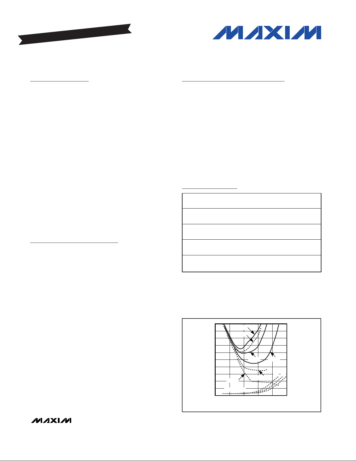
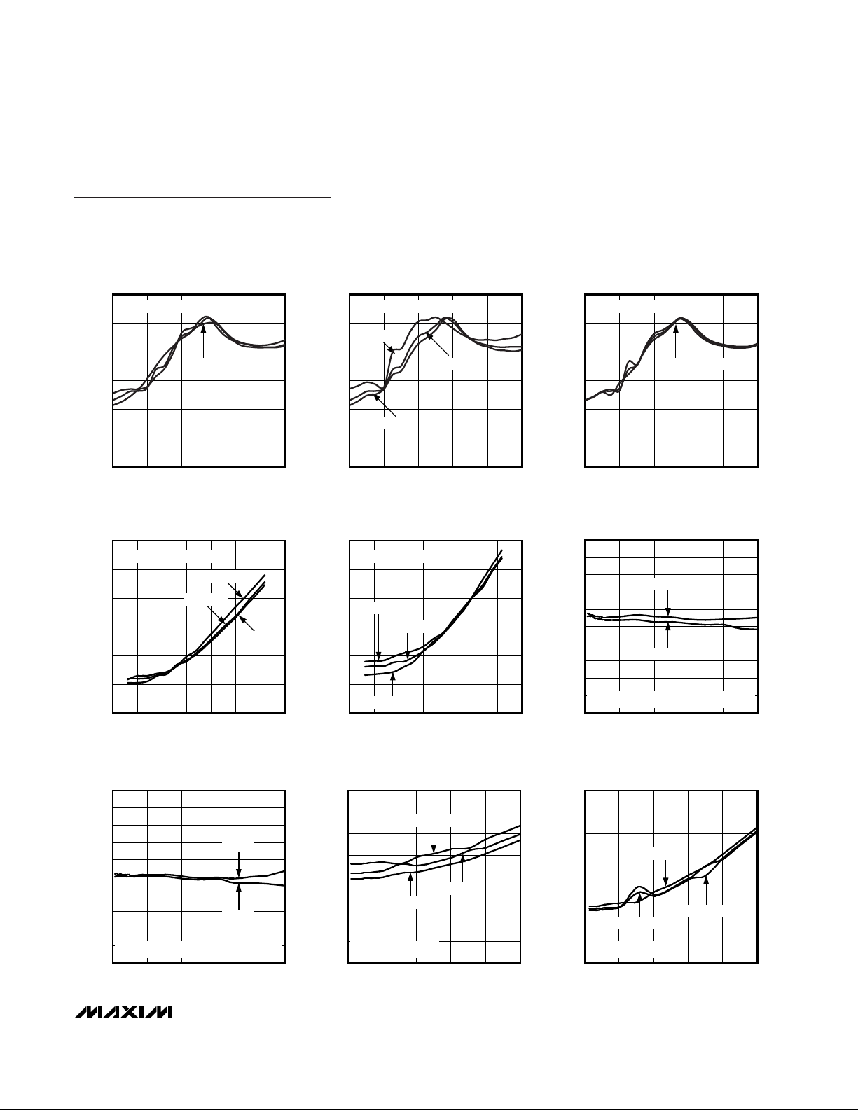
RF OUTPUT POWER PER CARRIER (dBm)
ACLR AND ALT CLR (dBc)
-10-20-30-40
-78
-76
-74
-72
-70
-68
-66
-64
-62
-60
-80
NOISE FLOOR (dBm/Hz)
-165
-155
-145
-135
-125
-175
-50 0
4C ADJ
4C ALT
2C ADJ 1C ADJ
2C ALT
1C ALT
4C
2C
1C
NOISE FLOOR
WCDMA, ACLR, ALTCLR and Noise vs. RF
Output Power at 2140MHz for Single,
Two, and Four Carriers
Ordering Information
19-3572; Rev 0; 4/05
For pricing, delivery, and ordering information, please contact Maxim/Dallas Direct! at
1-888-629-4642, or visit Maxim’s website at www.maxim-ic.com.
EVALUATION KIT AVAILABLE
PART
TEMP RANGE
PIN-PACKAGE
PKG
CODE
MAX2022ETX
T3666-2
MAX2022ETX-T
T3666-2
MAX2022ETX+D
T3666-2
MAX2022ETX+TD
T3666-2
cdma2000 is a registered trademark of Telecommunications
Industry Association.
cdmaOne is a trademark of CDMA Development Group.
*EP = Exposed paddle. + = Lead free. D = Dry pack.
-T = Tape-and-reel package.
-40°C to +85°C
-40°C to +85°C
-40°C to +85°C
-40°C to +85°C
36 Thin QFN-EP*
(6mm x 6mm)
36 Thin QFN-EP*
(6mm x 6mm)
36 Thin QFN-EP*
(6mm x 6mm)
36 Thin QFN-EP*
(6mm x 6mm)
Page 2
MAX2022
High-Dynamic-Range, Direct Upconversion
1500MHz to 2500MHz Quadrature Modulator
2 _______________________________________________________________________________________
ABSOLUTE MAXIMUM RATINGS
Stresses beyond those listed under “Absolute Maximum Ratings” may cause permanent damage to the device. These are stress ratings only, and functional
operation of the device at these or any other conditions beyond those indicated in the operational sections of the specifications is not implied. Exposure to
absolute maximum rating conditions for extended periods may affect device reliability.
VCC_ to GND ........................................................-0.3V to +5.5V
COMP .............................................................................0 to V
CC
BBIP, BBIN, BBQP, BBQN to GND ............-2.5V to (VCC+ 0.3V)
LO, RFOUT to GND Maximum Current ...............................50mA
Baseband Differential I/Q Input Power (Note A) ............+20dBm
LO Input Power...............................................................+10dBm
RBIASLO1 Maximum Current .............................................10mA
RBIASLO2 Maximum Current .............................................10mA
RBIASLO3 Maximum Current .............................................10mA
θJA(without air flow) ..........................................…………34°C/W
θ
JA
(2.5m/s air flow) .........................................................28°C/W
θ
JC
(junction to exposed paddle) ...................................8.5°C/W
Junction Temperature......................................................+150°C
Storage Temperature Range .............................-65°C to +150°C
Lead Temperature (soldering 10s, non-lead free)...........+245°C
Lead Temperature (soldering 10s, lead free) ..................+260°C
DC ELECTRICAL CHARACTERISTICS
(MAX2022 Typical Application Circuit, VCC= +4.75V to +5.25V, GND = 0V, I/Q inputs terminated into 100Ω differential, LO input terminated into 50Ω, RF output terminated into 50Ω, R1 = 432Ω, R2 = 562Ω, R3 = 301Ω, T
C
= -40°C to +85°C, unless otherwise noted.
Typical values are at V
CC
= +5V, TC= +25°C, unless otherwise noted.) (Note 1)
PARAMETER
SYMBOL
CONDITIONS
MIN
TYP
MAX
UNITS
Supply Voltage V
CC
V
Total Supply Current I
TOTAL
Pins 3, 13, 15, 31, 33 all connected to V
CC
342 mA
Total Power Dissipation
mW
Note A: Maximum reliable continuous power applied to the baseband differential port is +12dBm from an external 100Ω source.
AC ELECTRICAL CHARACTERISTICS
(MAX2022 Typical Application Circuit, VCC= +4.75V to +5.25V, GND = 0V, I/Q differential inputs driven from a 100Ω DC-coupled
source, 0V common-mode input, P
LO
= 0dBm, 1900MHz ≤ fLO≤ 2200MHz, 50Ω LO and RF system impedance, R1 = 432Ω, R2 =
562Ω, R3 = 301Ω, T
C
= -40°C to +85°C. Typical values are at VCC= +5V, V
BBI
= 109mV
P-P
differential, V
BBQ
= 109mV
P-P
differential,
f
IQ
= 1MHz, TC= +25°C, unless otherwise noted.) (Note 1)
PARAMETER
SYMBOL
CONDITIONS
MIN
TYP
MAX
UNITS
BASEBAND INPUT
Baseband Input Differential
Impedance
f
IQ
= 1MHz 43 Ω
BB Common-Mode Input Voltage
Range
0
V
Output Power TC = +25°C -24
dBm
RF OUTPUTS (fLO = 1960MHz)
Output IP3
V
BBI
, V
BBQ
= 547mV
P-P
differential per tone
into 50Ω,
f
BB1
= 1.8MHz,
f
BB2
= 1.9MHz
21.8
dBm
Output IP2
V
BBI
, V
BBQ
= 547mV
P-P
differential per tone
into 50Ω,
f
BB1
= 1.8MHz,
f
BB2
= 1.9MHz
48.9
dBm
Output Power
dBm
4.75 5.00 5.25
292
1460 1796
-2.5
-20.5
+1.5
Page 3
MAX2022
High-Dynamic-Range, Direct Upconversion
1500MHz to 2500MHz Quadrature Modulator
_______________________________________________________________________________________ 3
AC ELECTRICAL CHARACTERISTICS (continued)
(MAX2022 Typical Application Circuit, VCC= +4.75V to +5.25V, GND = 0V, I/Q differential inputs driven from a 100Ω DC-coupled
source, 0V common-mode input, P
LO
= 0dBm, 1900MHz ≤ fLO≤ 2200MHz, 50Ω LO and RF system impedance, R1 = 432Ω, R2 =
562Ω, R3 = 301Ω, T
C
= -40°C to +85°C. Typical values are at VCC= +5V, V
BBI
= 109mV
P-P
differential, V
BBQ
= 109mV
P-P
differential,
f
IQ
= 1MHz, TC= +25°C, unless otherwise noted.) (Note 1)
PARAMETER
CONDITIONS
TYP
UNITS
Output Power Variation Over
Temperature
T
C
= -40°C to +85°C
dB/°C
Output-Power Flatness
f
LO
= 1960MHz, sweep fBB,
P
RF
flatness for fBB from 1MHz to 50MHz
0.6 dB
ACLR (1st Adjacent Channel
5MHz Offset)
Single-carrier WCDMA (Note 2),
RFOUT = -16dBm
70 dBc
LO Leakage
No external calibration, with each baseband
input terminated in 50Ω
dBm
Sideband Suppression No external calibration 47.3 dBc
Output Return Loss 15.3 dB
Output Noise Density
f
meas
= 2060MHz, with each baseband
input terminated in 50Ω
dBm/Hz
LO Input Return Loss 10.1 dB
RF OUTPUTS (fLO = 2140MHz)
Output IP3
V
BBI
, V
BBQ
= 547mV
P-P
differential per tone
into 50Ω,
f
BB1
= 1.8MHz,
f
BB2
= 1.9MHz
23.3
dBm
Output IP2
V
BBI
, V
BBQ
= 547mV
P-P
differential per tone
into 50Ω,
f
BB1
= 1.8MHz,
f
BB2
= 1.9MHZ
51.5
dBm
Output Power
dBm
Output Power Variation Over
Temperature
T
C
= -40°C to +85°C
dB/°C
Output-Power Flatness
f
LO
= 2140MHz,
sweep f
BB
,
P
RF
flatness for fBB from 1MHz to 50MHz
0.32 dB
ACLR (1st Adjacent Channel
5MHz Offset)
Single-carrier WCDMA (Note 2),
RFOUT = -16dBm, f
LO
= 2GHz
70 dBc
LO Leakage
No external calibration, with each baseband
input terminated in 50Ω
dBm
Sideband Suppression No external calibration 45.7 dBc
Output Return Loss 13.5 dB
Output Noise Density
f
meas
= 2240MHz, with each baseband
input terminated in 50Ω
dBm/Hz
LO Input Return Loss 18.1 dB
Note 1: TCis the temperature on the exposed paddle.
Note 2: Single-carrier WCDMA peak-to-average ratio of 10.5dB for 0.1% complimentary cumulative distribution function.
SYMBOL
MIN
-0.004
-46.7
-173.4
-20.8
-0.005
-40.4
-173.2
MAX
Page 4
MAX2022
High-Dynamic-Range, Direct Upconversion
1500MHz to 2500MHz Quadrature Modulator
4 _______________________________________________________________________________________
Typical Operating Characteristics
(MAX2022 Typical Application Circuit, 50Ω LO input, R1 = 432Ω, R2 = 562Ω, R3 = 301Ω, VCC= +5V, PLO= 0dBm, V
IFI
= V
IFQ
=
109mV
P-P
differential, fIQ= 1MHz, I/Q differential inputs driven from a 100Ω DC-coupled source, common-mode input from 0V, TC=
+25°C, unless otherwise noted.)
ACLR vs. OUTPUT POWER
MAX2022 toc01
OUTPUT POWER (dBm)
ACLR (dB)
-10-20-30-40 0
-78
-76
-74
-72
-70
-68
-66
-64
-62
-60
-80
ADJACENT CHANNEL
ALTERNATE CHANNEL
SINGLE CARRIER
ACLR vs. OUTPUT POWER
MAX2022 toc02
OUTPUT POWER (dBm)
ACLR (dB)
-10-20-30-40 0
-78
-76
-74
-72
-70
-68
-66
-64
-62
-60
-80
ADJACENT CHANNEL
ALTERNATE CHANNEL
TWO CARRIER
ACLR vs. OUTPUT POWER
MAX2022 toc03
OUTPUT POWER (dBm)
ACLR (dB)
-20-30-40-50 -10
-78
-76
-74
-72
-70
-68
-66
-64
-62
-60
-80
ADJACENT CHANNEL
ALTERNATE CHANNEL
FOUR CARRIER
OUTPUT POWER vs. LO FREQUENCY
MAX2022 toc04
LO FREQUENCY (GHz)
OUTPUT POWER (dBm)
2.32.11.91.7
-7
-6
-5
-4
-3
-2
-8
1.5 2.5
VI = VQ = 0.611V
P-P
DIFFERENTIAL
PLO = -3dBm, 0dBm, +3dBm
OUTPUT POWER vs. LO FREQUENCY
MAX2022 toc05
LO FREQUENCY (GHz)
OUTPUT POWER (dBm)
2.32.11.91.7
-7
-6
-5
-4
-3
-2
-8
1.5 2.5
VI = VQ = 0.611V
P-P
DIFFERENTIAL
TC = +85°C
TC = +25°C
TC = -40°C
OUTPUT POWER vs. LO FREQUENCY
MAX2022 toc06
LO FREQUENCY (GHz)
OUTPUT POWER (dBm)
2.32.11.91.7
-7
-6
-5
-4
-3
-2
-8
1.5 2.5
VI = VQ = 0.611V
P-P
DIFFERENTIAL
VCC = 4.75V, 5.0V, 5.25V
LO LEAKAGE vs. LO FREQUENCY
MAX2022 toc07
LO FREQUENCY (GHz)
LO LEAKAGE (dBm)
2.32.11.91.7
-70
-50
-30
-10
-90
1.5 2.5
BASEBAND INPUTS TERMINATED IN 50
Ω
PLO = -3dBm, +3dBm
PLO = 0dBm
LO LEAKAGE vs. LO FREQUENCY
MAX2022 toc08
LO FREQUENCY (GHz)
LO LEAKAGE (dBm)
2.32.11.91.7
-70
-50
-30
-10
-90
1.5 2.5
BASEBAND INPUTS TERMINATED IN 50
Ω
TC = -40°C, +85°C
TC = +25°C
LO LEAKAGE vs. LO FREQUENCY
MAX2022 toc09
LO FREQUENCY (GHz)
LO LEAKAGE (dBm)
2.32.11.91.7
-70
-50
-30
-10
-90
1.5 2.5
BASEBAND INPUTS TERMINATED IN 50
Ω
VCC = 4.75V, 5.0V
VCC = 5.25V
Page 5
MAX2022
High-Dynamic-Range, Direct Upconversion
1500MHz to 2500MHz Quadrature Modulator
_______________________________________________________________________________________ 5
IMAGE REJECTION (dB)
10
20
30
40
50
60
0
IMAGE REJECTION vs. LO FREQUENCY
MAX2022 toc10
LO FREQUENCY (GHz)
2.32.11.91.71.5 2.5
fBB = 1MHz, VI = VQ = 112mV
P-P
TC = -40°C, +25°C, +85°C
IMAGE REJECTION (dB)
10
20
30
40
50
60
0
IMAGE REJECTION vs. LO FREQUENCY
MAX2022 toc11
LO FREQUENCY (GHz)
2.32.11.91.71.5 2.5
fBB = 1MHz, VI = VQ = 112mV
P-P
PLO = 0dBm
PLO = +3dBm
PLO = -3dBm
IMAGE REJECTION (dB)
10
20
30
40
50
60
0
IMAGE REJECTION vs. LO FREQUENCY
MAX2022 toc12
LO FREQUENCY (GHz)
2.32.11.91.71.5 2.5
fBB = 1MHz, VI = VQ = 112mV
P-P
VCC = 4.75, 5.0V, 5.25V
Typical Operating Characteristics (continued)
(MAX2022 Typical Application Circuit, 50Ω LO input, R1 = 432Ω, R2 = 562Ω, R3 = 301Ω, VCC= +5V, PLO= 0dBm, V
IFI
= V
IFQ
=
109mV
P-P
differential, fIQ= 1MHz, I/Q differential inputs driven from a 100Ω DC-coupled source, common-mode input from 0V, TC=
+25°C, unless otherwise noted.)
OUTPUT NOISE vs. OUTPUT POWER
AMX2022 toc13
OUTPUT POWER (dBm)
OUTPUT NOISE (dBm/Hz)
50-10 -5-15-20
-175
-170
-165
-160
-155
-150
-180
-25 10
PLO = 0dBm, fLO = 1960MHz
TC = +85°C
TC = -40°C
TC = +25°C
OUTPUT NOISE vs. OUTPUT POWER
AMX2022 toc14
OUTPUT POWER (dBm)
OUTPUT NOISE (dBm/Hz)
50-10 -5-15-20
-176
-172
-168
-164
-160
-156
-180
-25 10
PLO = 0dBm, fLO = 2140MHz
TC = -40°C
TC = +85°C
TC = +25°C
IF FLATNESS
vs. BASEBAND FREQUENCY
MAX2022 toc15
BASEBAND FREQUENCY (MHz)
IF POWER (dBm)
80604020
-23
-22
-21
-20
-19
-18
-17
-16
-15
-14
-24
0 100
fLO = 1960MHz, PBB = -12dBm/PORT INTO 50
Ω
fLO - f
RF
fLO + f
RF
IF FLATNESS
vs. BASEBAND FREQUENCY
MAX2022 toc16
BASEBAND FREQUENCY (MHz)
IF POWER (dBm)
80604020
-23
-22
-21
-20
-19
-18
-17
-16
-15
-14
-24
0 100
fLO = 2140MHz, PBB = -12dBm/PORT INTO 50Ω
fLO - f
RF
fLO + f
RF
BASEBAND DIFFERENTIAL INPUT RESISTANCE
vs. BASEBAND FREQUENCY
BASEBAND DIFFERENTIAL INPUT RESISTANCE (Ω)
41.5
42.0
42.5
43.0
43.5
44.0
44.5
45.0
41.0
MAX2022 toc17
BASEBAND FREQUENCY (MHz)
6040 80200100
fLO = 2GHz, PLO = 0dBm
VCC = 5.0V
VCC = 4.75V
VCC = 5.25V
BASEBAND DIFFERENTIAL INPUT RESISTANCE
vs. BASEBAND FREQUENCY
BASEBAND DIFFERENTIAL INPUT RESISTANCE (Ω)
43.0
43.5
44.0
44.5
42.5
MAX2022 toc18
BASEBAND FREQUENCY (MHz)
6040 80200100
fLO = 2GHz, VCC = 5.0V
PLO = -3dBm
PLO = +3dBm
PLO = 0dBm
Page 6

MAX2022
High-Dynamic-Range, Direct Upconversion
1500MHz to 2500MHz Quadrature Modulator
6 _______________________________________________________________________________________
OUTPUT IP3
vs. LO FREQUENCY
MAX2022 toc19
LO FREQUENCY (GHz)
OIP3 (dBm)
2.32.11.91.7
5
10
15
20
25
0
1.5 2.5
TC = -40°C, +25°C, +85°C
VBB = 0.61V
P-P
DIFFERENTIAL PER TONE,
f
BB1
= 1.8MHz, f
BB2
= 1.9MHz
OUTPUT IP3
vs. LO FREQUENCY
MAX2022 toc20
LO FREQUENCY (GHz)
OIP3 (dBm)
2.32.11.91.7
5
10
15
20
25
0
1.5 2.5
VBB = 0.61V
P-P
DIFFERENTIAL PER TONE,
f
BB1
= 1.8MHz, f
BB2
= 1.9MHz
VCC = 5.0V, 5.25V
VCC = 4.75V
OUTPUT IP3
vs. LO FREQUENCY
MAX2022 toc21
LO FREQUENCY (GHz)
OIP3 (dBm)
2.32.11.91.7
5
10
15
20
25
0
1.5 2.5
VBB = 0.61V
P-P
DIFFERENTIAL PER TONE,
f
BB1
= 1.8MHz, f
BB2
= 1.9MHz
PLO = 0dBm, +3dBm
PLO = -3dBm
COMMMON-MODE BASEBAND VOLTAGE (V)
210-1-2
10
20
30
40
50
60
0
-3 3
OUTPUT IP3
vs. COMMON-MODE BASEBAND VOLTAGE
MAX2022 toc22
OIP3 (dBm)
fLO = 2140MHz
fLO = 1960MHz
VBB = 0.61V
P-P
DIFFERENTIAL PER TONE,
f
BB1
= 1.8MHz, f
BB2
= 1.9MHz
10
20
30
40
50
60
70
0
OUTPUT IP2
vs. LO FREQUENCY
MAX2022 toc23
LO FREQUENCY (GHz)
OIP2 (dBm)
2.32.11.91.71.5 2.5
VBB = 0.61V
P-P
DIFFERENTIAL PER TONE,
f
BB1
= 1.8MHz, f
BB2
= 1.9MHz
TC = +25°C
TC = +85°C
TC = -40°C
10
20
30
40
50
60
70
0
OUTPUT IP2
vs. LO FREQUENCY
MAX2022 toc24
LO FREQUENCY (GHz)
OIP2 (dBm)
2.32.11.91.71.5 2.5
VBB = 0.61V
P-P
DIFFERENTIAL PER TONE,
f
BB1
= 1.8MHz, f
BB2
= 1.9MHz
VCC = 4.75V, 5.0V
VCC = 5.25V
10
20
30
40
50
60
70
0
OUTPUT IP2
vs. LO FREQUENCY
MAX2022 toc25
LO FREQUENCY (GHz)
OIP2 (dBm)
2.32.11.91.71.5 2.5
PLO = +3dBm
PLO = 0dBm
PLO = -3dBm
VBB = 0.61V
P-P
DIFFERENTIAL PER TONE,
f
BB1
= 1.8MHz, f
BB2
= 1.9MHz
COMMMON-MODE BASEBAND VOLTAGE (V)
210-1-2
10
20
30
40
50
60
0
-3 3
OUTPUT IP2
vs. COMMON-MODE BASEBAND VOLTAGE
MAX2022 toc26
OIP2 (dBm)
fLO = 2140MHz
fLO = 1960MHz
VBB = 0.61V
P-P
DIFFERENTIAL PER TONE,
f
BB1
= 1.8MHz, f
BB2
= 1.9MHz
LO LEAKAGE vs. LO FREQUENCY
MAX2022 toc27
LO FREQUENCY (GHz)
LO LEAKAGE (dBm)
1.9701.9651.9601.9551.950
-80
-60
-40
-20
0
-100
1.945 1.975
NULLED AT fLO = 1960MHz AT
P
RF
= -18dBm
Typical Operating Characteristics (continued)
(MAX2022 Typical Application Circuit, 50Ω LO input, R1 = 432Ω, R2 = 562Ω, R3 = 301Ω, VCC= +5V, PLO= 0dBm, V
IFI
= V
IFQ
=
109mV
P-P
differential, fIQ= 1MHz, I/Q differential inputs driven from a 100Ω DC-coupled source, common-mode input from 0V, TC=
+25°C, unless otherwise noted.)
Page 7

MAX2022
High-Dynamic-Range, Direct Upconversion
1500MHz to 2500MHz Quadrature Modulator
_______________________________________________________________________________________ 7
LO LEAKAGE vs. PRF WITH
LO LEAKAGE NULLED AT SPECIFIC P
RF
MAX2022 toc28
OUTPUT POWER PRF (dBm)
LO LEAKAGE (dBm)
-20-30 -25 -15-35
-88
-86
-84
-82
-80
-78
-76
-74
-72
-70
-68
-90
-40 -10
fLO = 1960MHz
NULLED AT -10dBm
NULLED AT -14dBm,
-18dBm, -22dBm
LO LEAKAGE vs. PRF WITH
LO LEAKAGE NULLED AT SPECIFIC P
RF
MAX2022 toc29
OUTPUT POWER PRF (dBm)
LO LEAKAGE (dBm)
-20-30 -25 -15-35
-88
-86
-84
-82
-80
-78
-76
-74
-72
-70
-68
-90
-40 -10
fLO = 2140Hz
NULLED AT -10dBm
NULLED AT -14dBm,
-18dBm, -22dBm
LO FREQUENCY (GHz)
2.05
2.001.951.90
-80
-70
-60
-50
-40
-30
-20
-10
0
-90
1.85 2.10
LO LEAKAGE vs. fLO WITH
LO LEAKAGE NULLED AT SPECIFIC P
RF
LO LEAKAGE (dBm)
fLO = 1960MHz, NULLED AT -10dBm P
RF
MAX2022 toc30
LO FREQUENCY (GHz)
2.20
2.152.102.05
-80
-70
-60
-50
-40
-30
-20
-10
0
-90
2.00 2.25
LO LEAKAGE vs. fLO WITH
LO LEAKAGE NULLED AT SPECIFIC P
RF
LO LEAKAGE (dBm)
fLO = 2140MHz, NULLED AT -10dBm P
RF
MAX2022 toc31
LO LEAKAGE vs. DIFFERENTIAL
DC OFFSET ON Q-SIDE
MAX2022 toc32
DC DIFFERENTIAL OFFSET ON Q-SIDE (mV)
LO LEAKAGE (dBm)
-9-10-11-12-13-14
-70
-60
-50
-40
-80
-15 -8
PRF = -18dBm, I-SIDE NULLED
fLO = 2140MHz
fLO = 1960MHz
SIDEBAND SUPRESSION vs. P
RF
MAX2022 toc33
MODULATOR P
OUT
(dBm)
SIDEBAND SUPPRESSION (dB)
-15-20-25
10
20
40
30
50
60
70
0
-30 -10
f
BB1
= 1.8MHz, f
BB2
= 9MHz, fLO = 1960MHz,
1.8MHz BASEBAND TONE NULLED AT
P
RF
= -20dBm
1.8MHz
9MHz
SIDEBAND SUPRESSION vs. P
RF
MAX2022 toc34
MODULATOR P
OUT
(dBm)
SIDEBAND SUPPRESSION (dB)
-15-20-25
10
20
30
40
50
60
70
0
-30 -10
f
BB1
= 1.8MHz, f
BB2
= 9MHz, fLO = 2140MHz,
1.8MHz BASEBAND TONE NULLED AT
P
RF
= -20dBm
1.8MHz
9MHz
RF PORT RETURN LOSS (dB)
-15
-10
-5
0
-20
RF PORT RETURN LOSS
vs. LO FREQUENCY
MAX2022 toc35
LO FREQUENCY (GHz)
2.32.11.91.71.5 2.5
VCC = 4.75V, 5.0V, 5.25V
-25
-20
-15
-10
-5
0
-30
LO PORT RETURN LOSS (dB)
LO PORT RETURN LOSS
vs. LO FREQUENCY
MAX2022 toc36
LO FREQUENCY (GHz)
2.32.11.91.71.5 2.5
VCC = 4.75V, 5.0V, 5.25V
Typical Operating Characteristics (continued)
(MAX2022 Typical Application Circuit, 50Ω LO input, R1 = 432Ω, R2 = 562Ω, R3 = 301Ω, VCC= +5V, PLO= 0dBm, V
IFI
= V
IFQ
=
109mV
P-P
differential, fIQ= 1MHz, I/Q differential inputs driven from a 100Ω DC-coupled source, common-mode input from 0V, TC=
+25°C, unless otherwise noted.)
Page 8

MAX2022
High-Dynamic-Range, Direct Upconversion
1500MHz to 2500MHz Quadrature Modulator
8 _______________________________________________________________________________________
-45
-40
-35
-30
-25
-20
-15
-10
-5
0
-50
LO PORT RETURN LOSS (dB)
LO PORT RETURN LOSS
vs. LO FREQUENCY
MAX2022 toc37
LO FREQUENCY (GHz)
2.32.11.91.71.5 2.5
PLO = -3dBm
PLO = +3dBm
PLO = 0dBm
OUTPUT POWER vs. INPUT POWER (PIN*)
MAX2022 toc38
INPUT POWER (PIN*) (dBm)
OUTPUT POWER (dBm)
1383
-8
-6
-4
-2
0
2
4
6
8
10
-10
-2 18
fLO = 1960MHz
*P
IN
IS THE AVAILABLE
POWER FROM ONE OF
THE FOUR 50
Ω
BASEBAND SOURCES
TC = -40°C, +25°C, +85°C
OUTPUT POWER vs. INPUT POWER (PIN*)
MAX2022 toc39
INPUT POWER (PIN*) (dBm)
OUTPUT POWER (dBm)
1383
-8
-6
-4
-2
0
2
4
6
8
10
-10
-2 18
PLO = 2140MHz
*P
IN
IS THE AVAILABLE
POWER FROM ONE OF
THE FOUR 50
Ω
BASEBAND SOURCES
TC = -40°C, +25°C, +85°C
TOTAL SUPPLY CURRENT
vs. TEMPERATURE (T
C
)
MAX2022 toc40
TEMPERATURE (°C)
TOTAL SUPPLY CURRENT (mA)
603510-15
260
280
300
320
340
240
-40 85
VCC = 5.25V
VCC = 4.75V
VCC = 5.0V
65
70
75
80
85
90
60
VCCLOA SUPPLY CURRENT
vs. TEMPERATURE (T
C
)
MAX2022 toc41
TEMPERATURE (°C)
VCCLOA SUPPLY CURRENT (mA)
603510-15-40 85
VCC = 5.25V
VCC = 4.75V
VCC = 5.0V
VCCLOI1 SUPPLY CURRENT
vs. TEMPERATURE (T
C
)
MAX2022 toc42
TEMPERATURE (°C)
VCCLOI1 SUPPLY CURRENT (mA)
603510-15
35
40
45
50
55
30
-40 85
VCC = 5.25V
VCC = 4.75V
VCC = 5.0V
45
50
55
60
65
70
40
VCCLOI2 SUPPLY CURRENT
vs. TEMPERATURE (T
C
)
MAX2022 toc43
TEMPERATURE (°C)
VCCLOI2 SUPPLY CURRENT (mA)
603510-15-40 85
VCC = 5.25V
VCC = 4.75V
VCC = 5.0V
VCCLOQ1 SUPPLY CURRENT
vs. TEMPERATURE (T
C
)
MAX2022 toc44
TEMPERATURE (°C)
VCCLOQ1 SUPPLY CURRENT (mA)
603510-15
35
40
45
50
55
30
-40 85
VCC = 5.25V
VCC = 4.75V
VCC = 5.0V
45
50
55
60
65
70
40
VCCLOQ2 SUPPLY CURRENT
vs. TEMPERATURE (T
C
)
MAX2022 toc45
TEMPERATURE (°C)
VCCLOQ2 SUPPLY CURRENT (mA)
603510-15-40 85
VCC = 5.25V
VCC = 4.75V
VCC = 5.0V
Typical Operating Characteristics (continued)
(MAX2022 Typical Application Circuit, 50Ω LO input, R1 = 432Ω, R2 = 562Ω, R3 = 301Ω, VCC= +5V, PLO= 0dBm, V
IFI
= V
IFQ
=
109mV
P-P
differential, fIQ= 1MHz, I/Q differential inputs driven from a 100Ω DC-coupled source, common-mode input from 0V, TC=
+25°C, unless otherwise noted.)
Page 9
MAX2022
High-Dynamic-Range, Direct Upconversion
1500MHz to 2500MHz Quadrature Modulator
_______________________________________________________________________________________ 9
MAX2022
Detailed Description
The MAX2022 is designed for upconverting differential
in-phase (I) and quadrature (Q) inputs from baseband to
a 1500MHz to 2500MHz RF frequency range.
Applications include single and multicarrier 1800MHz to
2200MHz UMTS/WCDMA, cdma2000, and DCS/PCS
base stations. Direct upconversion architectures are
advantageous since they significantly reduce transmitter
cost, part count, and power consumption as compared
to traditional IF-based double upconversion systems.
The MAX2022 integrates internal baluns, an LO buffer, a
phase splitter, two LO driver amplifiers, two matched
double-balanced passive mixers, and a wideband
quadrature combiner. Precision matching between the
in-phase and quadrature channels, and highly linear
mixers achieves excellent dynamic range, ACLR, 1dB
compression point, and LO and sideband suppression,
making it ideal for four-carrier WCDMA/UMTS operation.
LO Input Balun, LO Buffer, and
Phase Splitter
The MAX2022 requires a single-ended LO input, with a
nominal power of 0dBm. An internal low-loss balun at
the LO input converts the single-ended LO signal to a
differential signal at the LO buffer input. In addition, the
internal balun matches the buffer’s input impedance to
50Ω over the entire band of operation.
The output of the LO buffer goes through a phase splitter, which generates a second LO signal that is shifted
by 90° with respect to the original. The 0° and 90° LO
signals drive the I and Q mixers, respectively.
LO Driver
Following the phase splitter, the 0° and 90° LO signals
are each amplified by a two-stage amplifier to drive the
I and Q mixers. The amplifier boosts the level of the LO
signals to compensate for any changes in LO drive levels. The two-stage LO amplifier allows a wide input
power range for the LO drive. While a nominal LO
power of 0dBm is specified, the MAX2022 can tolerate
LO level swings from -3dBm to +3dBm.
I/Q Modulator
The MAX2022 modulator is composed of a pair of
matched double-balanced passive mixers and a balun.
The I and Q differential baseband inputs accept signals
from DC to beyond 100MHz with differential amplitudes
Pin Description
PIN NAME FUNCTION
1, 5, 9–12, 14,
16–19, 22, 24,
27–30, 32, 34,
35, 36
GND Ground
2 RBIASLO3 3rd LO Amplifier Bias. Connect a 301Ω resistor to ground.
3 VCCLOA LO Input Buffer Amplifier Supply Voltage
4 LO Local Oscillator Input. 50Ω input impedance.
6 RBIASLO1 1st LO Input Buffer Amplifier Bias. Connect a 432Ω resistor to ground.
7 COMP Compensation Capacitor Input. Connect a 22pF capacitor to ground.
8 RBIASLO2 2nd LO Amplifier Bias. Connect a 562Ω resistor to ground.
13 VCCLOI1 I-Channel 1st LO Amplifier Supply Voltage
15 VCCLOI2 I-Channel 2nd LO Amplifier Supply Voltage
20 BBIP Baseband In-Phase Positive Input
21 BBIN Baseband In-Phase Negative Input
23 RFOUT RF Output
25 BBQN Baseband Quadrature Negative Input
26 BBQP Baseband Quadrature Positive Input
31 VCCLOQ2 Q-Channel 1st LO Amplifier Supply Voltage
33 VCCLOQ1 Q-Channel 2nd LO Amplifier Supply Voltage
EP GND
Exposed Ground Paddle. The exposed paddle MUST be soldered to the ground plane using
multiple vias.
Page 10
MAX2022
up to 2V
P-P
differential (common-mode input equals 0V).
The wide input bandwidth allows for direct interface with
the baseband DACs. No active buffer circuitry between
the baseband DAC and the MAX2022 is required.
The I and Q signals directly modulate the 0° and 90°
LO signals and are upconverted to the RF frequency.
The outputs of the I and Q mixers are combined
through a balun to a singled-ended RF output.
Applications Information
LO Input Drive
The LO input of the MAX2022 requires a single-ended
drive at a 1500MHz to 2500MHz frequency. It is internally matched to 50Ω. An integrated balun converts the
singled-ended input signal to a differential signal at the
LO buffer differential input. An external DC-blocking
capacitor is the only external part required at this interface. The LO input power should be within the -3dBm
to +3dBm range.
COMP Pin
The COMP pin is used to provide additional lowpass filtering to the bias circuit noise. An external capacitor
can be used from the COMP pin to ground to reduce
the close-in noise of the modulator. For UMTS, connecting a 22pF capacitor from the COMP pin to ground is
recommended to filter out noise and frequency offsets
above 3.5MHz. For GSM, connecting a 1nF capacitor
from COMP to ground is recommended for filtering out
noise and frequency offsets above 600kHz.
Baseband I/Q Input Drive
The MAX2022 I and Q baseband inputs should be driven differentially for best performance. The baseband
inputs have a 50Ω differential input impedance. The
optimum source impedance for the I and Q inputs is
100Ω differential. This source impedance will achieve
the optimal signal transfer to the I and Q inputs, and the
optimum output RF impedance match. The MAX2022
can accept input power levels of up to +12dBm on the I
and Q inputs. Operation with complex waveforms, such
as CDMA or WCDMA carriers, utilize input power levels
that are far lower. This lower power operation is made
necessary by the high peak-to-average ratios of these
complex waveforms. The peak signals must be kept
below the compression level of the MAX2022. The input
common-mode voltage should be confined to the -2V to
+1.5V DC range.
The MAX2022 is designed to interface directly with
Maxim high-speed DACs. This generates an ideal total
transmitter lineup, with minimal ancillary circuit elements.
Such DACs include the MAX5875 series of dual DACs,
and the MAX5895 dual interpolating DAC. These DACs
have ground-referenced differential current outputs.
Typical termination of each DAC output into a 50Ω load
High-Dynamic-Range, Direct Upconversion
1500MHz to 2500MHz Quadrature Modulator
10 ______________________________________________________________________________________
MAX5895
DUAL 16-BIT INTERP DAC
MAX2022
RF MODULATOR
I/Q GAIN AND
OFFSET ADJUST
BBI
LO
BBQ
FREQ
50
Ω
50
Ω
50
Ω
FREQ
50
Ω
50
Ω
50Ω
50
Ω
0
°
90
°
∑
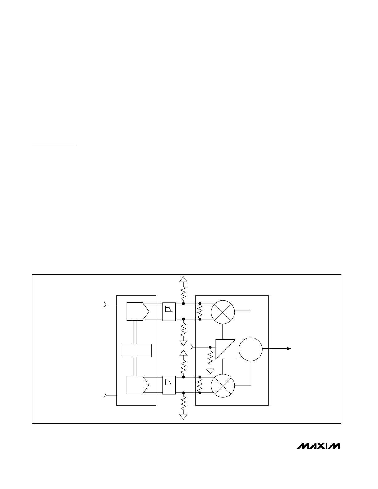
Figure 1. MAX5895 DAC Interfaced with MAX2022
Page 11

MAX2022
High-Dynamic-Range, Direct Upconversion
1500MHz to 2500MHz Quadrature Modulator
______________________________________________________________________________________ 11
resistor to ground, and a 10mA nominal DC output current results in a 0.5V common-mode DC level into the
modulator I/Q inputs. The nominal signal level provided
by the DACs will be in the -12dBm range for a single
CDMA or WCDMA carrier, reducing to -18dBm per carrier for a four-carrier application.
The I/Q input bandwidth is greater than 50MHz at
-0.1dB response. The direct connection of the DAC to
the MAX2022 insures the maximum signal fidelity, with
no performance-limiting baseband amplifiers required.
The DAC output can be passed through a lowpass filter
to remove the image frequencies from the DAC’s output
response. The MAX5895 dual interpolating DAC can be
operated at interpolation rates up to x8. This has the
benefit of moving the DAC image frequencies to a very
high, remote frequency, easing the design of the baseband filters. The DAC’s output noise floor and interpola-
tion filter stopband attenuation are sufficiently good to
insure that the 3GPP noise floor requirement is met for
large frequency offsets, 60MHz for example, with no filtering required on the RF output of the modulator.
Figure 1 illustrates the ease and efficiency of interfacing the MAX2022 with a Maxim DAC, in this case the
MAX5895 dual 16-bit interpolating-modulating DAC.
The MAX5895 DAC has programmable gain and differential offset controls built in. These can be used to optimize the LO leakage and sideband suppression of the
MAX2022 quadrature modulator.
RF Output
The MAX2022 utilizes an internal passive mixer architecture. This enables a very low noise floor of
-173.2dBm/Hz for low-level signals, below about
-20dBm output power level. For higher output level signals, the noise floor will be determined by the internal
LO noise level at approximately -162dBc/Hz.
The I/Q input power levels and the insertion loss of the
device will determine the RF output power level. The
input power is the function of the delivered input I and
Q voltages to the internal 50Ω termination. For simple
sinusoidal baseband signals, a level of 89mV
P-P
differ-
ential on the I and the Q inputs results in an input power
level of -17dBm delivered to the I and Q internal 50Ω
terminations. This results in a -27dBm RF output power.
Generation of WCDMA Carriers
The MAX2022 quadrature modulator makes an ideal
signal source for the generation of multiple WCDMA
carriers. The combination of high OIP3 and exceptionally low output noise floor gives an unprecedented output dynamic range. The output dynamic range allows
the generation of four WCDMA carriers in the UMTS
band with a noise floor sufficiently low to meet the
3GPP specification requirements with no additional RF
filtering. This promotes an extremely simple and efficient transmitter lineup. Figure 2 illustrates a complete
transmitter lineup for a multicarrier WCDMA transmitter
in the UMTS band.
The MAX5895 dual interpolating-modulating DAC is
operated as a baseband signal generator. For generation of four carriers of WCDMA modulation, and digital
predistortion, an input data rate of 61.44 or
122.88Mbps can be used. The DAC can then be programmed to operate in x8 or x4 interpolation mode,
resulting in a 491.52Msps output sample rate. The
DAC will generate four carriers of WCDMA modulation
MAX2022
MAX5895
MAX2022
RF-MODULATOR
MAX2057
TX
OUTPUT
+12dB
L-C FILTER
I/Q GAIN AND
OFFSET ADJUST
I
I
Q
Q
∑
CLOCK
SYNTH
Figure 2. Complete Transmitter Lineup for a Multicarrier WCDMA in the UMTS Band
Page 12

MAX2022
with an ACLR typically greater than 77dB under these
conditions. The output power will be approximately
-18dBm per carrier, with a noise floor typically less
than -144dBc/Hz.
The MAX5895 DAC has built-in gain and offset fine
adjustments. These are programmable by a 3-wire serial logic interface. The gain adjustment can be used to
adjust the relative gains of the I and Q DAC outputs.
This feature can be used to improve the native sideband suppression of the MAX2022 quadrature modulator. The gain adjustment resolution of 0.01dB allows
sideband nulling down to approximately -60dB. The offset adjustment can similarly be used to adjust the offset
DC output of each I and Q DAC. These offsets can then
be used to improve the native LO leakage of the
MAX2022. The DAC resolution of 4 LSBs will yield
nulled LO leakage of typically less than -50dBc relative
to four-carrier output levels.
The DAC outputs must be filtered by baseband filters to
remove the image frequency signal components. The
baseband signals for four-carrier operation cover DC to
10MHz. The image frequency appears at 481MHz to
491MHz. This very large frequency spread allows the
use of very low-complexity lowpass filters, with excellent in-band gain and phase performance. The low
DAC noise floor allows for the use of a very wideband
filter, since the filter is not necessary to meet the 3GPP
noise floor specification.
The MAX2022 quadrature modulator then upconverts the
baseband signals to the RF output frequency. The output
power of the MAX2022 will be approximately
-28dBm per carrier. The noise floor will be less than
-169dBm/Hz, with an ACLR typically greater than 65dBc.
This performance meets the 3GPP specification requirements with substantial margins. The noise floor performance will be maintained for large offset frequencies,
eliminating the need for subsequent RF filtering in the
transmitter lineup.
The RF output from the MAX2022 is then amplified by a
combination of a low-noise amplifier followed by a
MAX2057 RF-VGA. This VGA can be used for lineup
compensation for gain variance of transmitter and
power amplifier elements. No significant degradation of
the signal or noise levels will be incurred by this additional amplification. The MAX2057 will deliver an output
power of -6dBm per carrier, 0dBm total at an ACLR of
65dB and noise floor of -142dBc/Hz.
Layout Considerations
A properly designed PC board is an essential part of
any RF/microwave circuit. Keep RF signal lines as short
as possible to reduce losses, radiation, and inductance. For the best performance, route the ground pin
traces directly to the exposed pad under the package.
The PC board exposed paddle MUST be connected to
the ground plane of the PC board. It is suggested that
multiple vias be used to connect this pad to the lowerlevel ground planes. This method provides a good
RF/thermal conduction path for the device. Solder the
exposed pad on the bottom of the device package to
the PC board. The MAX2022 evaluation kit can be used
as a reference for board layout. Gerber files are available upon request at www.maxim-ic.com.
Power-Supply Bypassing
Proper voltage-supply bypassing is essential for highfrequency circuit stability. Bypass all VCCpins with
22pF and 0.1µF capacitors placed as close to the pins
as possible. The smallest capacitor should be placed
closest to the device.
To achieve optimum performance, use good voltagesupply layout techniques. The MAX2022 has several RF
processing stages that use the various VCCpins, and
while they have on-chip decoupling, off-chip interaction
between them may degrade gain, linearity, carrier suppression, and output power-control range. Excessive
coupling between stages may degrade stability.
Exposed Pad RF/Thermal Considerations
The EP of the MAX2022’s 36-pin thin QFN-EP package
provides a low thermal-resistance path to the die. It is
important that the PC board on which the IC is mounted
be designed to conduct heat from this contact. In addition, the EP provides a low-inductance RF ground path
for the device.
The exposed paddle (EP) MUST be soldered to a
ground plane on the PC board either directly or through
an array of plated via holes. An array of 9 vias, in a 3 x
3 array, is suggested. Soldering the pad to ground is
critical for efficient heat transfer. Use a solid ground
plane wherever possible.
High-Dynamic-Range, Direct Upconversion
1500MHz to 2500MHz Quadrature Modulator
12 ______________________________________________________________________________________
Page 13

MAX2022
High-Dynamic-Range, Direct Upconversion
1500MHz to 2500MHz Quadrature Modulator
______________________________________________________________________________________ 13
Package Information
For the latest package outline information, go to
www.maxim-ic.com/packages
.
1
2
3
4
5
6
7
8
9
10
11 12
13 14
THIN QFN
15
16 17
18
27
26
25
24
23
22
21
20
19
36
35
34
33 32
31
30 29
28
Σ
BIAS
LO2
BIAS
LO1
90°
0°
BIAS
LO3
GND
BBIP
BBIN
GND
RFOUT
GND
BBQN
BBQP
GND
GND
GND
GND
GND
GND
GND
GND
GND
GND
RBIASLO3
VCCLOA
LO
GND
RBIASLO1
COMP
RBIASLO2
GND
GND
GND
VCCLOQ2
GND
GND
GND
GND
MAX2022
VCCLOI1
VCCLOI1
VCCLOQ1
Pin Configuration/Functional Diagram
Chip Information
TRANSISTOR COUNT: 1414
PROCESS: SiGe BiCMOS
Page 14

High-Dynamic-Range, Direct Upconversion
1500MHz to 2500MHz Quadrature Modulator
Maxim cannot assume responsibility for use of any circuitry other than circuitry entirely embodied in a Maxim product. No circuit patent licenses are
implied. Maxim reserves the right to change the circuitry and specifications without notice at any time.
14 ____________________Maxim Integrated Products, 120 San Gabriel Drive, Sunnyvale, CA 94086 408-737-7600
© 2005 Maxim Integrated Products Printed USA is a registered trademark of Maxim Integrated Products, Inc.
MAX2022
1
2
3
4
5
6
7
8
9
10
11 12
13 14 15
16 17
18
27
26
25
24
23
22
21
20
19
36
35
34
33 32
31
30 29
28
Σ
BIAS
LO2
BIAS
LO1
90°
0°
BIAS
LO3
GND
BBIP
BBIN
GND
RFOUT
GND
BBQN
BBQP
Q+
Q-
GND
I-
I+
C9
1.2pF
C8
0.1µF
V
CC
C7
22pF
C5
0.1µF
C6
22pF
V
CC
GND
GND
GND
GND
VCCLOI1
VCCLOI2
GND
GND
GND
GND
GND
RBIASLO3
R3
301Ω
C1
22pF
C3
22pF
C2
0.1µF
V
CC
VCCLOA
LO
GND
RBIASLO1
R1
432Ω
C4
22pF
COMP
RBIASLO2
C11
0.1µF
V
CC
C10
22pF
C12
0.1µF
C13
22pF
V
CC
GND
GND
GND
VCCLOQ2
GND
GND
GND
GND
MAX2022
VCCLOQ1
R2
562Ω
Typical Application Circuit
COMPONENT VALUE DESCRIPTION
22pF 22pF ±5%, 50V C0G ceramic capacitors (0402)
C2, C5, C8, C11, C12 0.1µF 0.1µF ±10%, 16V X7R ceramic capacitors (0603)
C9 1.2pF 1.2pF ±0.1pF, 50V C0G ceramic capacitor (0402)
R1 432Ω 432Ω ±1% resistor (0402)
R2 562Ω 562Ω ±1% resistor (0402)
R3 301Ω 301Ω ±1% resistor (0402)
Table 1. Component List Referring to the Typical Application Circuit
C1, C3, C4, C6, C7, C10, C13
 Loading...