

Page 1
General Description
The MAX19996 single, high-linearity downconversion
mixer provides 8.7dB conversion gain, +24.5dBm IIP3,
and 9.6dB noise figure for 2000MHz to 3000MHz WCS,
LTE, WiMAX™, and MMDS wireless infrastructure applications. With an 1800MHz to 2550MHz LO frequency
range, this particular mixer is ideal for low-side LO
injection receiver architectures. High-side LO injection
is supported by the MAX19996A, which is pin-for-pin
and functionally compatible with the MAX19996.
In addition to offering excellent linearity and noise performance, the MAX19996 also yields a high level of component integration. This device includes a double-balanced
passive mixer core, an IF amplifier, and an LO buffer.
On-chip baluns are also integrated to allow for singleended RF and LO inputs. The MAX19996 requires a
nominal LO drive of 0dBm, and supply current is typically 230mA at V
CC
= +5.0V or 149.5mA at VCC= +3.3V.
The MAX19996 is pin compatible with the MAX19996A
2300MHz to 3900MHz mixer. The device is also pin similar with the MAX9984/MAX9986 400MHz to 1000MHz
mixers and the MAX9993/MAX9994/MAX9996 1700MHz
to 2200MHz mixers, making this entire family of downconverters ideal for applications where a common PCB
layout is used for multiple frequency bands.
The MAX19996 is available in a compact 5mm x 5mm,
20-pin thin QFN lead-free package with an exposed
pad. Electrical performance is guaranteed over the
extended -40°C to +85°C temperature range.
Applications
2.3GHz WCS Base Stations
2.5GHz WiMAX and LTE Base Stations
2.7GHz MMDS Base Stations
Fixed Broadband Wireless Access
Wireless Local Loop
Private Mobile Radios
Military Systems
Features
♦ 2000MHz to 3000MHz RF Frequency Range
♦ 1800MHz to 2550MHz LO Frequency Range
♦ 50MHz to 500MHz IF Frequency Range
♦ 8.7dB Typical Conversion Gain
♦ 9.6dB Typical Noise Figure
♦ +24.5dBm Typical Input IP3
♦ +11dBm Typical Input 1dB Compression Point
♦ 69dBc Typical 2RF-2LO Spurious Rejection at
P
RF
= -10dBm
♦ Integrated LO Buffer
♦ Integrated RF and LO Baluns for Single-Ended
Inputs
♦ Low -3dBm to +3dBm LO Drive
♦ Pin Compatible with the MAX19996A 2300MHz to
3900MHz Mixer
♦ Pin Similar with the MAX9993/MAX9994/
MAX9996 1700MHz to 2200MHz Mixers and
MAX9984/MAX9986 400MHz to 1000MHz Mixers
♦ Single +5.0V or +3.3V Supply
♦ External Current-Setting Resistors Provide Option
for Operating Device in Reduced-Power/ReducedPerformance Mode
MAX19996
SiGe High-Linearity, 2000MHz to 3000MHz
Downconversion Mixer with LO Buffer
________________________________________________________________
Maxim Integrated Products
1
Ordering Information
19-4177; Rev 0; 7/08
For pricing, delivery, and ordering information, please contact Maxim Direct at 1-888-629-4642,
or visit Maxim’s website at www.maxim-ic.com.
PART TEMP RANGE PIN-PACKAGE
MAX19996ETP+ -40°C to +85°C 20 Thin QFN-EP*
MAX19996ETP+T -40°C to +85°C 20 Thin QFN-EP*
+
Denotes a lead-free/RoHS-compliant package.
*
EP = Exposed pad.
T = Tape and reel.
Pin Configuration appears at end of data sheet.
WiMAX is a trademark of WiMAX Forum.
Page 2
MAX19996
SiGe High-Linearity, 2000MHz to 3000MHz
Downconversion Mixer with LO Buffer
2 _______________________________________________________________________________________
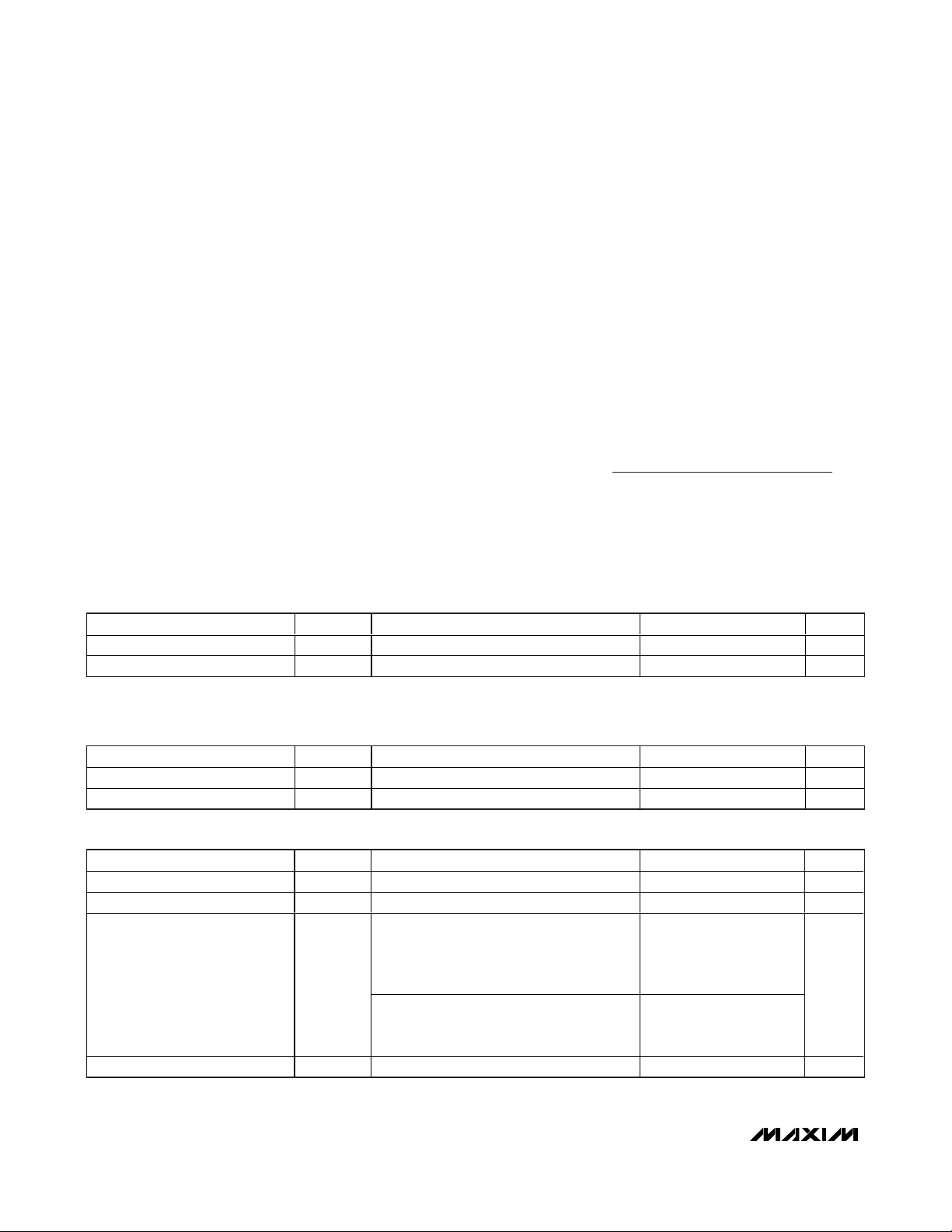
ABSOLUTE MAXIMUM RATINGS
+3.3V SUPPLY DC ELECTRICAL CHARACTERISTICS
(
Typical Application Circuit
, VCC= +3.0V to +3.6V, no input AC signals. TC= -40°C to +85°C, unless otherwise noted. Typical values
are at V
CC
= +3.3V, TC= +25°C, parameters are guaranteed by design and not production tested, unless otherwise noted.)
Stresses beyond those listed under “Absolute Maximum Ratings” may cause permanent damage to the device. These are stress ratings only, and functional
operation of the device at these or any other conditions beyond those indicated in the operational sections of the specifications is not implied. Exposure to
absolute maximum rating conditions for extended periods may affect device reliability.
VCCto GND...........................................................-0.3V to +5.5V
IF+, IF-, LOBIAS, LO, IFBIAS,
LEXT to GND ..........................................-0.3V to (V
CC
+ 0.3V)
RF, LO Input Power ........................................................+12dBm
RF, LO Current
(RF and LO is DC shorted to GND through a balun) ......50mA
Continuous Power Dissipation (Note 1) ..............................5.0W
θ
JA
(Notes 2, 3)..............................................................+38°C/W
θ
JC
(Notes 1, 3)................................................................13°C/W
Operating Case Temperature
Range (Note 4)........................................T
C
= -40°C to +85°C
Junction Temperature......................................................+150°C
Storage Temperature Range .............................-65°C to +150°C
Lead Temperature (soldering, 10s) .................................+300°C
+5.0V SUPPLY DC ELECTRICAL CHARACTERISTICS
(
Typical Application Circuit
, VCC= +4.75V to +5.25V, no input AC signals. TC= -40°C to +85°C, unless otherwise noted. Typical val-
ues are at V
CC
= +5.0V, TC= +25°C, all parameters are production tested.) (Note 6)
RECOMMENDED AC OPERATING CONDITIONS
Note 1: Based on junction temperature TJ= TC+ (θJCx VCCx ICC). This formula can be used when the temperature of the exposed
pad is known while the device is soldered down to a PCB. See the
Applications Information
section for details. The junction
temperature must not exceed +150°C.
Note 2: Junction temperature T
J
= TA+ (θJAx VCCx ICC). This formula can be used when the ambient temperature of the PCB is
known. The junction temperature must not exceed +150°C.
Note 3: Package thermal resistances were obtained using the method described in JEDEC specification JESD51-7, using a four-
layer board. For detailed information on package thermal considerations, refer to www.maxim-ic.com/thermal-tutorial
.
Note 4: T
C
is the temperature on the exposed pad of the package. TAis the ambient temperature of the device and PCB.
Supply Voltage V
Supply Current I
PARAMETER SYMBOL CONDITIONS MIN TYP MAX UNITS
CC
CC
4.75 5 5.25 V
230 245 mA
Supply Voltage V
Supply Current I
PARAMETER SYMBOL CONDITIONS MIN TYP MAX UNITS
CC
CC
Total supply current, VCC = +3.3V 149.5 mA
3.0 3.3 3.6 V
PARAMETER SYMBOL CONDITIONS MIN TYP MAX UNITS
RF Frequency f
LO Frequency f
IF Frequency f
LO Drive Level P
RF
LO
IF
LO
(Note 7) 2000 3000 MHz
(Note 7) 1800 2550 MHz
U si ng M i ni - C i r cui ts TC 4- 1W- 17 4:1 tr ansfor m er
as d efi ned i n the Typ i cal Ap p l i cati on C i r cui t, IF
m atchi ng com p onents affect the IF fr eq uency
r ang e ( N ote 7)
U si ng al ter nati ve M i ni - C i r cui ts TC 4- 1W- 7A
4:1 transformer, IF matching components
affect the IF frequency range (Note 7)
100 500
50 250
-3 +3 dBm
MHz
Page 3
MAX19996
SiGe High-Linearity, 2000MHz to 3000MHz
Downconversion Mixer with LO Buffer
_______________________________________________________________________________________ 3
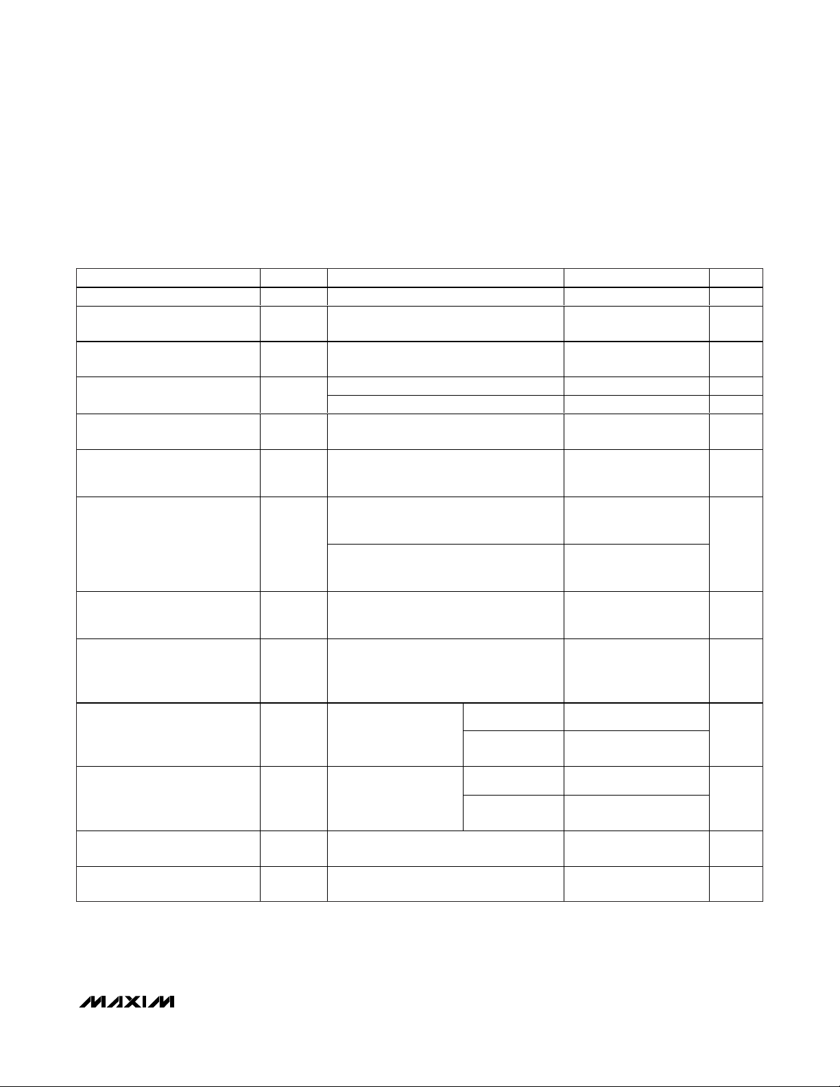
+5.0V SUPPLY AC ELECTRICAL CHARACTERISTICS
(
Typical Application Circuit
, VCC= +4.75V to +5.25V, RF and LO ports are driven from 50Ω sources, PLO= -3dBm to +3dBm,
P
RF
= -5dBm, fRF= 2300MHz to 2800MHz, fLO= 2000MHz to 2500MHz, fIF= 300MHz, fRF> fLO, TC= -40°C to +85°C. Typical val-
ues are at V
CC
= +5.0V, PRF= -5dBm, PLO= 0dBm, fRF= 2500MHz, fLO= 2200MHz, fIF= 300MHz, TC= +25°C, all parameters are
guaranteed by design and characterization, unless otherwise noted.) (Note 6)
PARAMETER SYMBOL CONDITIONS MIN TYP MAX UNITS
Conversion Power Gain G
Conversion Power Gain Variation
vs. Frequency
Conversion Power Gain
Temperature Coefficient
Input 1dB Compression Point IP
Third-Order Input Intercept Point IIP3
Third-Order Input Intercept Point
Variation Over Temperature
Noise Figure NF
Noise Figure Temperature
Coefficient
Noise Figure Under Blocking
Condition
2RF-2LO Spur Rejection 2 x 2
3RF-3LO Spur Rejection 3 x 3
RF Input Return Loss
LO Input Return Loss
TC = +25°C (Note 5) 8.1 8.7 9.3 dB
C
∆G
TC
1dB
fRF = 2300MHz to 2800MHz for any
C
100MHz band
TC = -40°C to +85°C -0.012 dB/°C
G
0.1 dB
TC = +25°C (Note 8) 10 11 dBm
fRF = 2500MHz, TC = +25°C (Note 8) 10.4 11 dBm
f
- f
RF1
T
f
RF
f
RF1
T
C
C
= 1MHz, P
RF2
= +25°C (Note 5)
= 2300MHz to 2800MHz, fIF = 300MHz,
- f
= 1MHz, P
RF2
= -40°C to +85°C
RF1
RF1
= P
= P
= -5dBm,
RF2
= -5dBm,
RF2
22 24.5 dBm
±0.5 dB
fRF = 2300MHz to 2700MHz, fIF = 300MHz,
single sideband, no blockers present
(Note 9)
SSB
f
= 2500M H z, f
R F
V
= +5.0V, TC = +25°C, single sideband,
CC
= 300M H z, P
I F
= 0d Bm ,
L O
9.6 12
9.6 10.5
no blockers present (Note 9)
fRF = 2000MHz to 3000MHz, single
TC
NF
sideband, no blockers present,
NF
T
= -40°C to +85°C (Note 9)
C
+8dBm blocker tone applied to RF port, f
= 2300MHz, fLO = 2110MHz, f
B
2400MHz, P
T
= +25°C (Note 9)
C
= 2300MHz to
f
RF
2700MHz, f
= -3dBm, VCC = +5.0V,
LO
=
LO
2000MHz to 2400MHz,
f
= f
SPUR
= 2300MHz to
f
RF
2700MHz, f
+ 150MHz
LO
LO
=
2000MHz to 2400MHz,
f
= f
SPUR
+ 100MHz
LO
LO on and IF terminated into a matched
impedance
RF and IF terminated into a matched
impedance
0.0183 dB/°C
RF
BLOCKER
=
20.8 25 dB
PRF = -10dBm 60 69
= -5dBm
P
RF
(Note 5)
55 64
PRF = -10dBm 70 78
= -5dBm
P
RF
(Note 5)
60 68
18 dB
20 dB
dB
dBc
dBc
Page 4
MAX19996
SiGe High-Linearity, 2000MHz to 3000MHz
Downconversion Mixer with LO Buffer
4 _______________________________________________________________________________________
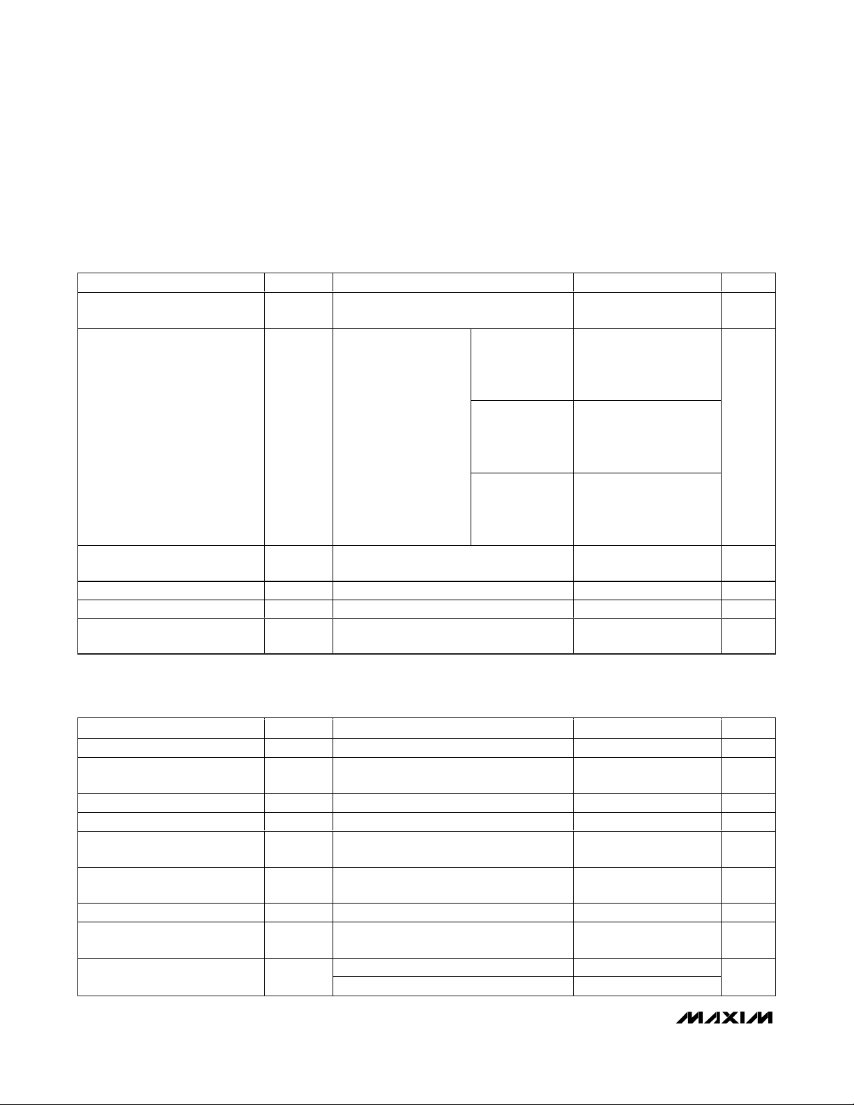
+5.0V SUPPLY AC ELECTRICAL CHARACTERISTICS (continued)
(
Typical Application Circuit
, VCC= +4.75V to +5.25V, RF and LO ports are driven from 50Ω sources, PLO= -3dBm to +3dBm,
P
RF
= -5dBm, fRF= 2300MHz to 2800MHz, fLO= 2000MHz to 2500MHz, fIF= 300MHz, fRF> fLO, TC= -40°C to +85°C. Typical val-
ues are at V
CC
= +5.0V, PRF= -5dBm, PLO= 0dBm, fRF= 2500MHz, fLO= 2200MHz, fIF= 300MHz, TC= +25°C, all parameters are
guaranteed by design and characterization, unless otherwise noted.) (Note 6)
+3.3V SUPPLY AC ELECTRICAL CHARACTERISTICS
(
Typical Application Circuit
, RF and LO ports are driven from 50Ω sources, Typical values are at VCC= +3.3V, PRF= -5dBm,
P
LO
= 0dBm, fRF= 2500MHz, fLO= 2200MHz, fIF= 300MHz, TC= +25°C, unless otherwise noted.) (Note 6)
IF Output Impedance Z
PARAMETER SYMBOL CONDITIONS MIN TYP MAX UNITS
Nominal differential impedance at the IC’s
IF
IF outputs
200 Ω
IF Output Return Loss
Minimum RF-to-IF Isolation
Maximum LO Leakage at RF Port fLO = 1900MHz to 2500MHz, PLO = +3dBm -22.7 dBm
M axi m um 2LO Leakag e at RF P or tf
Maximum LO Leakage at IF Port
RF terminated into 50Ω,
LO driven by 50Ω
source, IF transformed
to 50Ω using external
components shown in
the Typical Application
Circuit. See the IF Port
Return Loss vs. IF
Frequency graph in the
Typical Operating
Characteristics for
performance vs.
inductor values
f
= 2300MHz to 2700MHz, PLO = +3dBm
RF
(Note 5)
= 1900MHz to 2500MHz, P
LO
f
= 1900MHz to 2500MHz, P
LO
(Note 5)
fIF = 450MHz,
L1 = L2 = 120nH
fIF = 350MHz,
L1 = L2 = 270nH
= 300MHz,
f
IF
L1 = L2 = 470nH
= +3dBm -21 dBm
LO
= +3dBm
LO
25
25
25
34 dB
-27.5 dBm
Conversion Power Gain G
Conversion Power Gain Variation
vs. Frequency
Gain Variation Over Temperature TC
Input 1dB Compression Point IP
Third-Order Input Intercept Point IIP3
Third-Order Input Intercept
Variation Over Temperature
Noise Figure NF
Noise Figure Temperature
Coefficient
2RF-2LO Spur Rejection 2 x 2
PARAMETER SYMBOL CONDITIONS MIN TYP MAX UNITS
8.6 dB
0.1 dB
19.8 dBm
±0.5 dB
0.017 dB/°C
∆G
TC
C
C
G
1dB
SSB
NF
fRF = 2300MHz to 2800MHz for any
100MHz band
TC = -40°C to +85°C -0.012 dB/°C
(Note 8) 7.5 dBm
f
= 2500MHz, f
RF1
2200MHz, P
f
= 2500M H z, f
RF1
2200M H z, P
S i ng l e si d eb and , no b l ocker s p r esent ( N ote 9) 9.6 dB
Single sideband, no blockers present,
T
= -40°C to +85°C (Note 9)
C
PRF = -10dBm 65.9
= -5dBm 60.9
P
RF
RF1
RF1
= 2501MHz, fLO =
RF2
= P
= -5dBm
RF2
= 2501M H z, fLO =
RF2
= P
= - 5d Bm , T
RF2
= + 25°C
C
dB
dBc
Page 5
MAX19996
SiGe High-Linearity, 2000MHz to 3000MHz
Downconversion Mixer with LO Buffer
_______________________________________________________________________________________ 5
Note 5: 100% production tested for functional performance.
Note 6: All limits reflect losses of external components, including a 0.8dB loss at f
IF
= 300MHz due to the 4:1 impedance trans-
former. Output measurements were taken at IF outputs of the
Typical Application Circuit
.
Note 7: Not production tested. Operation outside this range is possible, but with degraded performance of some parameters. See
the
Typical Operating Characteristics
.
Note 8: Maximum reliable continuous input power applied to the RF or IF port of this device is +12dBm from a 50Ω source.
Note 9: Measured with external LO source noise filtered so that the noise floor is -174dBm/Hz. This specification reflects the
effects of all SNR degradations in the mixer including the LO noise, as defined in Application Note 2021:
Specifications
and Measurement of Local Oscillator Noise in Integrated Circuit Base Station Mixers
.
+3.3V SUPPLY AC ELECTRICAL CHARACTERISTICS (continued)
(
Typical Application Circuit
, RF and LO ports are driven from 50Ω sources, Typical values are at VCC= +3.3V, PRF= -5dBm,
P
LO
= 0dBm, fRF= 2500MHz, fLO= 2200MHz, fIF= 300MHz, TC= +25°C, unless otherwise noted.) (Note 6)
3RF-3LO Spur Rejection 3 x 3
RF Input Return Loss
LO Input Return Loss
IF Output Impedance Z
IF Output Return Loss
PARAMETER SYMBOL CONDITIONS MIN TYP MAX UNITS
P
= -10dBm 67.9
RF
= -5dBm 57.9
P
RF
LO on and IF terminated into a matched
impedance
RF and IF terminated into a matched
impedance
Nominal differential impedance at the IC’s
IF
IF outputs
RF ter m i nated i nto 50Ω ,
LO d r i ven b y 50Ω sour ce,
IF tr ansfor m ed to 50Ω
usi ng exter nal
com p onents show n i n the
Typ i cal Ap p l i cati on
C i r cui t. S ee the IF P or t
Retur n Loss vs. IF
Fr eq uency g r ap h i n the
Typ i cal Op er ati ng
C har acter i sti cs for
p er for m ance vs. i nd uctor
val ues.
fIF = 450MHz,
L1 = L2 = 120nH
fIF = 350MHz,
L1 = L2 = 270nH
f
= 300MHz,
IF
L1 = L2 = 470nH
dBc
16 dB
16.7 dB
200 Ω
23
23
23
dB
Minimum RF-to-IF Isolation fRF = 2300MHz to 2700MHz, PLO = +3dBm 33 dB
Maximum LO Leakage at RF Port fLO = 1900MHz to 2500MHz, PLO = +3dBm -26.6 dBm
M axi m um 2LO Leakag e at RF P or tf
Maximum LO Leakage at IF Port fLO = 1900MHz to 2500MHz, PLO = +3dBm -21.9 dBm
= 1900MHz to 2500MHz, PLO = +3dBm -28.8 dBm
LO
Page 6
MAX19996
SiGe High-Linearity, 2000MHz to 3000MHz
Downconversion Mixer with LO Buffer
6 _______________________________________________________________________________________
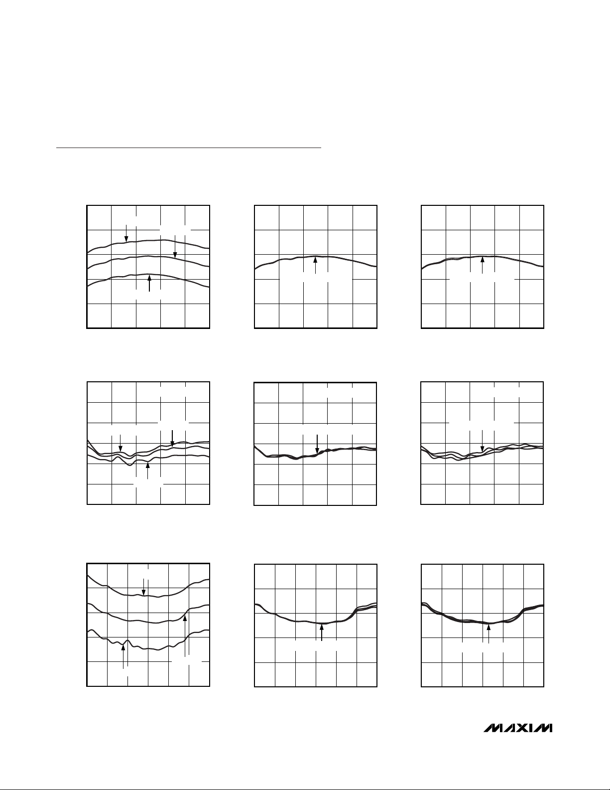
Typical Operating Characteristics
(
Typical Application Circuit
, VCC= +5.0V, PLO= 0dBm, PRF= -5dBm, LO is low-side injected for a 300MHz IF, TC = +25°C, unless
otherwise noted.)
CONVERSION GAIN vs. RF FREQUENCY
11
10
9
8
CONVERSION GAIN (dB)
7
6
2000 2200 2400 2600 2800 3000
TC = -40°C
TC = +85°C
RF FREQUENCY (MHz)
INPUT IP3 vs. RF FREQUENCY
28
27
26
25
INPUT IP3 (dBm)
24
23
TC = +85°C
TC = -40°C
TC = +25°C
PRF = -5dBm/TONE
TC = +25°C
11
MAX19996 toc01
10
9
8
CONVERSION GAIN (dB)
7
6
28
27
MAX19996 toc04
26
25
INPUT IP3 (dBm)
24
23
CONVERSION GAIN vs. RF FREQUENCY
PLO = -3dBm, 0dBm, +3dBm
2000 2200 2400 2600 2800 3000
RF FREQUENCY (MHz)
INPUT IP3 vs. RF FREQUENCY
PRF = -5dBm/TONE
PLO = -3dBm, 0dBm, +3dBm
11
MAX19996 toc02
10
9
8
CONVERSION GAIN (dB)
7
6
28
27
MAX19996 toc05
26
25
INPUT IP3 (dBm)
24
23
CONVERSION GAIN vs. RF FREQUENCY
MAX19996 toc03
VCC = 4.75V, 5.0V, 5.25V
2000 2200 2400 2600 2800 3000
RF FREQUENCY (MHz)
INPUT IP3 vs. RF FREQUENCY
PRF = -5dBm/TONE
MAX19996 toc06
VCC = 4.75V, 5.0V, 5.25V
MAX19996 toc08
NOISE FIGURE (dB)
22
2000 2200 2400 2600 2800 3000
RF FREQUENCY (MHz)
NOISE FIGURE vs. RF FREQUENCY
12
11
10
9
VCC = 4.75V, 5.0V, 5.25V
8
7
1800 2000 2200 2400 2600 2800 3000
RF FREQUENCY (MHz)
22
2000 2200 2400 2600 2800 3000
RF FREQUENCY (MHz)
NOISE FIGURE vs. RF FREQUENCY
12
TC = +85°C
11
10
9
NOISE FIGURE (dB)
8
TC = -40°C
7
1800 2000 2200 2400 2600 2800 3000
RF FREQUENCY (MHz)
TC = +25°C
MAX19996 toc07
NOISE FIGURE (dB)
22
2000 2200 2400 2600 2800 3000
RF FREQUENCY (MHz)
NOISE FIGURE vs. RF FREQUENCY
12
11
10
9
8
7
1800 2000 2200 2400 2600 2800 3000
PLO = -3dBm, 0dBm, +3dBm
RF FREQUENCY (MHz)
MAX19996 toc09
Page 7

Typical Operating Characteristics (continued)
(
Typical Application Circuit
, VCC= +5.0V, PLO= 0dBm, PRF= -5dBm, LO is low-side injected for a 300MHz IF, TC = +25°C, unless
otherwise noted.)
MAX19996
SiGe High-Linearity, 2000MHz to 3000MHz
Downconversion Mixer with LO Buffer
_______________________________________________________________________________________
7
2RF-2LO RESPONSE vs. RF FREQUENCY
85
75
65
2RF-2LO RESPONSE (dBc)
55
45
2000 2200 2400 2600 2800 3000
TC = +85°C
TC = -40°C
RF FREQUENCY (MHz)
TC = +25°C
3RF-3LO RESPONSE vs. RF FREQUENCY
85
80
75
2RF-2LO RESPONSE vs. RF FREQUENCY
85
75
65
2RF-2LO RESPONSE (dBc)
55
45
2000 2200 2400 2600 2800 3000
VCC = 4.75V, 5.0V, 5.25V
RF FREQUENCY (MHz)
PRF = -5dBm
3RF-3LO RESPONSE vs. RF FREQUENCY
85
80
75
PRF = -5dBm
PRF = -5dBm
PRF = -5dBm
TC = -40°C
2RF-2LO RESPONSE vs. RF FREQUENCY
85
MAX19996 toc10
75
65
2RF-2LO RESPONSE (dBc)
55
45
2000 2200 2400 2600 2800 3000
3RF-3LO RESPONSE vs. RF FREQUENCY
85
80
MAX19996 toc13
75
PLO = -3dBm
RF FREQUENCY (MHz)
PRF = -5dBm
PLO = +3dBm
PLO = 0dBm
PRF = -5dBm
MAX19996 toc11
MAX19996 toc14
MAX19996 toc12
MAX19996 toc15
70
65
3RF-3LO RESPONSE (dBc)
TC = +25°C
60
55
2000 2200 2400 2600 2800 3000
INPUT P
14
13
12
(dBm)
1dB
11
INPUT P
10
TC = -40°C
9
8
2000 2200 2400 2600 2800 3000
TC = +85°C
RF FREQUENCY (MHz)
vs. RF FREQUENCY
1dB
TC = +85°C
TC = +25°C
RF FREQUENCY (MHz)
70
65
3RF-3LO RESPONSE (dBc)
60
55
2000 2200 2400 2600 2800 3000
14
13
MAX19996 toc16
12
(dBm)
1dB
11
INPUT P
10
9
8
2000 2200 2400 2600 2800 3000
PLO = -3dBm, 0dBm, +3dBm
RF FREQUENCY (MHz)
INPUT P
vs. RF FREQUENCY
1dB
PLO = -3dBm, 0dBm, +3dBm
RF FREQUENCY (MHz)
70
65
3RF-3LO RESPONSE (dBc)
60
55
2000 2200 2400 2600 2800 3000
14
13
MAX19996 toc17
12
(dBm)
1dB
11
INPUT P
10
9
8
2000 2200 2400 2600 2800 3000
VCC = 4.75V, 5.0V, 5.25V
RF FREQUENCY (MHz)
INPUT P
1dB
VCC = 4.75V
RF FREQUENCY (MHz)
vs. RF FREQUENCY
VCC = 5.25V
VCC = 5.0V
MAX19996 toc18
Page 8

MAX19996
SiGe High-Linearity, 2000MHz to 3000MHz
Downconversion Mixer with LO Buffer
8 _______________________________________________________________________________________
Typical Operating Characteristics (continued)
(
Typical Application Circuit
, VCC= +5.0V, PLO= 0dBm, PRF= -5dBm, LO is low-side injected for a 300MHz IF, TC = +25°C, unless
otherwise noted.)
LO LEAKAGE AT IF PORT
vs. LO FREQUENCY
LO FREQUENCY (MHz)
LO LEAKAGE AT IF PORT (dBm)
MAX19996 toc19
1700 1900 2100 2300 2500 2700
-40
-30
-20
-10
0
TC = +85°C
TC = +25°C
TC = -40°C
LO LEAKAGE AT IF PORT
vs. LO FREQUENCY
LO FREQUENCY (MHz)
LO LEAKAGE AT IF PORT (dBm)
MAX19996 toc20
1700 1900 2100 2300 2500 2700
-40
-30
-20
-10
0
PLO = -3dBm, 0dBm, +3dBm
LO LEAKAGE AT IF PORT
vs. LO FREQUENCY
LO FREQUENCY (MHz)
LO LEAKAGE AT IF PORT (dBm)
MAX19996 toc21
1700 1900 2100 2300 2500 2700
-40
-30
-20
-10
0
VCC = 4.75V, 5.0V, 5.25V
RF-TO-IF ISOLATION vs. RF FREQUENCY
RF FREQUENCY (MHz)
RF-TO-IF ISOLATION (dB)
MAX19996 toc22
2000 2200 2400 2600 2800 3000
10
20
30
40
50
60
70
TC = -40°C
TC = +25°C
TC = +85°C
RF-TO-IF ISOLATION vs. RF FREQUENCY
RF FREQUENCY (MHz)
RF-TO-IF ISOLATION (dB)
MAX19996 toc23
2000 2200 2400 2600 2800 3000
10
20
30
40
50
60
70
PLO = -3dBm, 0dBm, +3dBm
RF-TO-IF ISOLATION vs. RF FREQUENCY
RF FREQUENCY (MHz)
RF-TO-IF ISOLATION (dB)
MAX19996 toc24
2000 2200 2400 2600 2800 3000
10
20
30
40
50
60
70
VCC = 4.75V
VCC = 5.0V
VCC = 5.25V
LO LEAKAGE AT RF PORT
vs. LO FREQUENCY
LO FREQUENCY (MHz)
LO LEAKAGE AT RF PORT (dBm)
MAX19996 toc25
1600 1800 2000 2200 2400 2600 2800 3000
-40
-35
-30
-25
-20
-15
-10
TC = -40°C, +25°C, +85°C
LO LEAKAGE AT RF PORT
vs. LO FREQUENCY
LO FREQUENCY (MHz)
LO LEAKAGE AT RF PORT (dBm)
MAX19996 toc26
1600 1800 2000 2200 2400 2600 2800 3000
-40
-35
-30
-25
-20
-15
-10
PLO = -3dBm, 0dBm, +3dBm
LO LEAKAGE AT RF PORT
vs. LO FREQUENCY
LO FREQUENCY (MHz)
LO LEAKAGE AT RF PORT (dBm)
MAX19996 toc27
1600 1800 2000 2200 2400 2600 2800 3000
-40
-35
-30
-25
-20
-15
-10
VCC = 4.75V
VCC = 5.0V, 5.25V
Page 9

MAX19996
SiGe High-Linearity, 2000MHz to 3000MHz
Downconversion Mixer with LO Buffer
_______________________________________________________________________________________
9
Typical Operating Characteristics (continued)
(
Typical Application Circuit
, VCC= +5.0V, PLO= 0dBm, PRF= -5dBm, LO is low-side injected for a 300MHz IF, TC = +25°C, unless
otherwise noted.)
RF PORT RETURN LOSS
vs. RF FREQUENCY
0
10
20
PLO = -3dBm, 0dBm, +3dBm
30
RF PORT RETURN LOSS (dB)
40
2000 2200 2400 2600 2800 3000
RF FREQUENCY (MHz)
SUPPLY CURRENT
vs. TEMPERATURE (T
250
IF PORT RETURN LOSS
vs. IF FREQUENCY
0
5
MAX19996 toc28
10
15
20
IF PORT RETURN LOSS (dB)
25
30
50 140 230 320 410 500
L1, L2 = 270nH
L1, L2 = 470nH
VCC = 4.75V, 5.0V, 5.25V
fLO = 2400MHz
L1, L2 = 120nH
IF FREQUENCY (MHz)
MAX19996 toc29
LO SELECTED RETURN LOSS (dB)
LO LEAKAGE AT IF PORT
)
C
0
vs. LO FREQUENCY
LO SELECTED RETURN LOSS
vs. LO FREQUENCY
0
10
PLO = 0dBm
20
30
40
1600 1800 2000 2200 2400 2600 2800 3000
PLO = +3dBm
PLO = -3dBm
LO FREQUENCY (MHz)
RF-TO-IF ISOLATION
vs. RF FREQUENCY
70
MAX9996 toc30
240
230
220
SUPPLY CURRENT (mA)
210
200
VCC = 5.25V
VCC = 5.0V
VCC = 4.75V
-40 -15 10 35 60 85
TEMPERATURE (°C)
MAX19996 toc31
-10
-20
-30
LO LEAKAGE AT IF PORT (dBm)
-40
1700 1900 2100 2300 2500 2700
L3 = 0Ω
L3 = 4.7nH
LO FREQUENCY (MHz)
60
MAX19996 toc32
50
40
30
RF-TO-IF ISOLATION (dB)
20
10
2000 2200 2400 2600 2800 3000
MAX19996 toc33
L3 = 4.7nH
L3 = 0Ω
RF FREQUENCY (MHz)
Page 10

MAX19996
SiGe High-Linearity, 2000MHz to 3000MHz
Downconversion Mixer with LO Buffer
10 ______________________________________________________________________________________
Typical Operating Characteristics (continued)
(
Typical Application Circuit
, VCC= +3.3V, PLO= 0dBm, PRF= -5dBm, LO is low-side injected for a 300MHz IF, TC = +25°C, unless
otherwise noted.)
CONVERSION GAIN
vs. RF FREQUENCY
11
10
TC = -40°C
9
CONVERSION GAIN
vs. RF FREQUENCY
VCC = 3.3V
TC = +25°C
MAX19996 toc34
CONVERSION GAIN
vs. RF FREQUENCY
MAX19996 toc35
11
10
9
11
10
9
VCC = 3.3V
MAX19996 toc36
8
CONVERSION GAIN (dB)
7
6
2000 2200 2400 2600 2800 3000
TC = +85°C
RF FREQUENCY (MHz)
INPUT IP3 vs. RF FREQUENCY
22
PRF = -5dBm/TONE
21
TC = +25°C
20
19
INPUT IP3 (dBm)
18
17
16
2000 2200 2400 2600 2800 3000
TC = +85°C
TC = -40°C
RF FREQUENCY (MHz)
NOISE FIGURE vs. RF FREQUENCY
12
11
10
TC = +85°C
TC = +25°C
VCC = 3.3V
VCC = 3.3V
CONVERSION GAIN (dB)
22
21
MAX19996 toc37
20
19
INPUT IP3 (dBm)
18
17
16
12
MAX19996 toc40
11
10
8
7
6
2000 2200 2400 2600 2800 3000
PLO = -3dBm, 0dBm, +3dBm
RF FREQUENCY (MHz)
INPUT IP3 vs. RF FREQUENCY
PRF = -5dBm/TONE
PLO = -3dBm, 0dBm, +3dBm
2000 2200 2400 2600 2800 3000
RF FREQUENCY (MHz)
VCC = 3.3V
NOISE FIGURE vs. RF FREQUENCY
VCC = 3.3V
PLO = -3dBm, 0dBm, +3dBm
CONVERSION GAIN (dB)
22
21
MAX19996 toc38
20
19
INPUT IP3 (dBm)
18
17
16
12
MAX19996 toc41
11
10
8
VCC = 3.0V, 3.3V, 3.6V
7
6
2000 2200 2400 2600 2800 3000
RF FREQUENCY (MHz)
INPUT IP3 vs. RF FREQUENCY
PRF = -5dBm/TONE
MAX19996 toc39
VCC = 3.0V, 3.3V, 3.6V
2000 2200 2400 2600 2800 3000
RF FREQUENCY (MHz)
NOISE FIGURE vs. RF FREQUENCY
MAX19996 toc42
VCC = 3.0V, 3.3V, 3.6V
9
NOISE FIGURE (dB)
8
TC = -40°C
7
1800 2000 2200 2400 2600 2800 3000
RF FREQUENCY (MHz)
9
NOISE FIGURE (dB)
8
7
1800 2000 2200 2400 2600 2800 3000
RF FREQUENCY (MHz)
9
NOISE FIGURE (dB)
8
7
1800 2000 2200 2400 2600 2800 3000
RF FREQUENCY (MHz)
Page 11

MAX19996
SiGe High-Linearity, 2000MHz to 3000MHz
Downconversion Mixer with LO Buffer
______________________________________________________________________________________
11
Typical Operating Characteristics (continued)
(
Typical Application Circuit
, VCC= +3.3V, PLO= 0dBm, PRF= -5dBm, LO is low-side injected for a 300MHz IF, TC = +25°C, unless
otherwise noted.)
2RF-2LO RESPONSE vs. RF FREQUENCY
85
75
65
2RF-2LO RESPONSE (dBc)
55
45
2000 2200 2400 2600 2800 3000
TC = +85°C
TC = +25°C
RF FREQUENCY (MHz)
3RF-3LO RESPONSE vs. RF FREQUENCY
70
65
TC = +25°C
60
TC = +85°C
TC = -40°C
PRF = -5dBm
VCC = 3.3V
PRF = -5dBm
VCC = 3.3V
85
MAX19996 toc43
75
65
2RF-2LO RESPONSE (dBc)
55
45
2000 2200 2400 2600 2800 3000
70
65
MAX19996 toc46
60
2RF-2LO RESPONSE vs. RF FREQUENCY
PRF = -5dBm
VCC = 3.3V
PLO = +3dBm
PLO = -3dBm
PLO = 0dBm
RF FREQUENCY (MHz)
3RF-3LO RESPONSE vs. RF FREQUENCY
PRF = -5dBm
VCC = 3.3V
MAX19996 toc44
MAX19996 toc47
2RF-2LO RESPONSE vs. RF FREQUENCY
85
75
65
2RF-2LO RESPONSE (dBc)
55
45
2000 2200 2400 2600 2800 3000
VCC = 3.0V, 3.3V, 3.6V
RF FREQUENCY (MHz)
PRF = -5dBm
3RF-3LO RESPONSE vs. RF FREQUENCY
70
65
60
PRF = -5dBm
MAX19996 toc45
MAX19996 toc48
55
50
3RF-3LO RESPONSE (dBc)
(dBm)
1dB
INPUT P
TC = -40°C
45
40
2000 2200 2400 2600 2800 3000
RF FREQUENCY (MHz)
INPUT P
10
9
8
7
6
5
2000 2200 2400 2600 2800 3000
vs. RF FREQUENCY
1dB
TC = +85°C
TC = -40°C
RF FREQUENCY (MHz)
TC = +25°C
VCC = 3.3V
55
50
3RF-3LO RESPONSE (dBc)
45
40
2000 2200 2400 2600 2800 3000
10
MAX19996 toc49
9
8
(dBm)
1dB
7
INPUT P
6
5
2000 2200 2400 2600 2800 3000
PLO = -3dBm, 0dBm, +3dBm
RF FREQUENCY (MHz)
INPUT P
vs. RF FREQUENCY
1dB
PLO = -3dBm, 0dBm, +3dBm
RF FREQUENCY (MHz)
VCC = 3.3V
55
50
3RF-3LO RESPONSE (dBc)
45
40
2000 2200 2400 2600 2800 3000
10
MAX19996 toc50
9
8
(dBm)
1dB
7
INPUT P
6
5
2000 2200 2400 2600 2800 3000
VCC = 3.0V, 3.3V, 3.6V
RF FREQUENCY (MHz)
INPUT P
1dB
VCC = 3.0V
RF FREQUENCY (MHz)
vs. RF FREQUENCY
VCC = 3.6V
VCC = 3.3V
MAX19996 toc51
Page 12

MAX19996
SiGe High-Linearity, 2000MHz to 3000MHz
Downconversion Mixer with LO Buffer
12 ______________________________________________________________________________________
Typical Operating Characteristics (continued)
(
Typical Application Circuit
, VCC= +3.3V, PLO= 0dBm, PRF= -5dBm, LO is low-side injected for a 300MHz IF, TC = +25°C, unless
otherwise noted.)
LO LEAKAGE AT IF PORT
vs. LO FREQUENCY
0
-10
-20
TC = +25°C
VCC = 3.3V
TC = -40°C
MAX19996 toc52
-10
-20
LO LEAKAGE AT IF PORT
vs. LO FREQUENCY
0
PLO = -3dBm, 0dBm, +3dBm
VCC = 3.3V
MAX19996 toc53
0
-10
-20
LO LEAKAGE AT IF PORT
vs. LO FREQUENCY
MAX19996 toc54
VCC = 3.0V, 3.3V, 3.6V
-30
LO LEAKAGE AT IF PORT (dBm)
TC = +85°C
-40
1700 1900 2100 2300 2500 2700
LO FREQUENCY (MHz)
RF-TO-IF ISOLATION vs. RF FREQUENCY
60
TC = +85°C
50
40
RF-TO-IF ISOLATION (dB)
30
20
TC = +25°C
TC = -40°C
2000 2200 2400 2600 2800 3000
RF FREQUENCY (MHz)
LO LEAKAGE AT RF PORT
vs. LO FREQUENCY
-20
-25
TC = -40°C, +25°C, +85°C
VCC = 3.3V
VCC = 3.3V
-30
LO LEAKAGE AT IF PORT (dBm)
-40
1700 1900 2100 2300 2500 2700
RF-TO-IF ISOLATION vs. RF FREQUENCY
60
MAX19996 toc55
50
40
RF-TO-IF ISOLATION (dB)
30
20
2000 2200 2400 2600 2800 3000
-20
MAX19996 toc58
-25
LO FREQUENCY (MHz)
VCC = 3.3V
PLO = -3dBm, 0dBm, +3dBm
RF FREQUENCY (MHz)
LO LEAKAGE AT RF PORT
vs. LO FREQUENCY
VCC = 3.3V
-30
LO LEAKAGE AT IF PORT (dBm)
-40
1700 1900 2100 2300 2500 2700
RF-TO-IF ISOLATION vs. RF FREQUENCY
60
MAX19996 toc56
50
40
RF-TO-IF ISOLATION (dB)
30
20
2000 2200 2400 2600 2800 3000
-20
VCC = 3.6V
MAX19996 toc59
-25
LO FREQUENCY (MHz)
VCC = 3.0V, 3.3V, 3.6V
RF FREQUENCY (MHz)
LO LEAKAGE AT RF PORT
vs. LO FREQUENCY
VCC = 3.3V
MAX19996 toc57
MAX19996 toc60
-30
-35
LO LEAKAGE AT RF PORT (dBm)
-40
1600 1800 2000 2200 2400 2600 2800 3000
LO FREQUENCY (MHz)
-30
-35
LO LEAKAGE AT RF PORT (dBm)
-40
1600 1800 2000 2200 2400 2600 2800 3000
PLO = -3dBm, 0dBm, +3dBm
LO FREQUENCY (MHz)
-30
VCC = 3.0V
-35
LO LEAKAGE AT RF PORT (dBm)
-40
1600 1800 2000 2200 2400 2600 2800 3000
LO FREQUENCY (MHz)
Page 13

MAX19996
SiGe High-Linearity, 2000MHz to 3000MHz
Downconversion Mixer with LO Buffer
______________________________________________________________________________________
13
Typical Operating Characteristics (continued)
(
Typical Application Circuit
, VCC= +3.3V, PLO= 0dBm, PRF= -5dBm, LO is low-side injected for a 300MHz IF, TC = +25°C, unless
otherwise noted.)
RF PORT RETURN LOSS
vs. RF FREQUENCY
0
5
10
15
20
RF PORT RETURN LOSS (dB)
25
30
2000 2200 2400 2600 2800 3000
PLO = -3dBm, 0dBm, +3dBm
RF FREQUENCY (MHz)
SUPPLY CURRENT
vs. TEMPERATURE (T
160
VCC = 3.6V
155
150
145
SUPPLY CURRENT (mA)
140
VCC = 3.3V
LO RETURN LOSS
vs. LO FREQUENCY
PLO = 0dBm
LO FREQUENCY (MHz)
vs. RF FREQUENCY
PRF = -5dBm/TONE
L3 = 4.7nH
PLO = +3dBm
VCC = 3.3V
PLO = -3dBm
INPUT IP3
VCC = 3.3V
VCC = 3.3V
C
VCC = 3.0V
IF PORT RETURN LOSS
vs. IF FREQUENCY
0
MAX19996 toc61
5
10
15
20
IF PORT RETURN LOSS (dB)
25
30
50 140 230 320 410 500
VCC = 3.0V, 3.3V, 3.6V
fLO = 2400MHz
MAX19996 toc62
L1, L2 = 120nH
L1, L2 = 270nH
L1, L2 = 470nH
IF FREQUENCY (MHz)
0
10
20
LO RETURN LOSS (dB)
30
40
1600 1800 2000 2200 2400 2600 2800 3000
CONVERSION GAIN
)
11
MAX19996 toc64
10
9
8
CONVERSION GAIN (dB)
7
vs. RF FREQUENCY
L3 = 0Ω, 4.7nH
VCC = 3.3V
MAX19996 toc65
22
21
20
19
INPUT IP3 (dBm)
18
17
MAX19996 toc63
MAX19996 toc66
135
-40 -15 10 35 60 85
TEMPERATURE (°C)
6
2000 2200 2400 2600 2800 3000
RF FREQUENCY (MHz)
16
2000 2200 2400 2600 2800 3000
RF FREQUENCY (MHz)
Page 14

MAX19996
SiGe High-Linearity, 2000MHz to 3000MHz
Downconversion Mixer with LO Buffer
14 ______________________________________________________________________________________
Typical Operating Characteristics (continued)
(
Typical Application Circuit
, VCC= +3.3V, PLO= 0dBm, PRF= -5dBm, LO is low-side injected for a 300MHz IF, TC = +25°C, unless
otherwise noted.)
75
70
65
60
55
2RF-2LO RESPONSE (dBc)
-10
-20
-30
LO LEAKAGE AT IF PORT (dBm)
-40
L3 = 4.7nH
50
45
2000 2200 2400 2600 2800 3000
0
1700 1900 2100 2300 2500 2700
2RF-2LO RESPONSE
vs. RF FREQUENCY
L3 = 0Ω
RF FREQUENCY (MHz)
PRF = -5dBm
VCC = 3.3V
LO LEAKAGE AT IF PORT
vs. LO FREQUENCY
L3 = 0Ω
L3 = 4.7nH
LO FREQUENCY (MHz)
VCC = 3.3V
MAX19996 toc67
MAX19996 toc69
3RF-3LO RESPONSE
vs. RF FREQUENCY
75
70
65
60
55
3RF-3LO RESPONSE (dBc)
50
45
2000 2200 2400 2600 2800 3000
L3 = 0Ω
L3 = 4.7nH
RF FREQUENCY (MHz)
PRF = -5dBm
VCC = 3.3V
RF-TO-IF ISOLATION
vs. RF FREQUENCY
60
50
40
30
RF-TO-IF ISOLATION (dB)
20
10
2000 2200 2400 2600 2800 3000
L3 = 4.7nH
L3 = 0Ω
RF FREQENCY (MHz)
MAX19996 toc68
VCC = 3.3V
MAX19996 toc70
Page 15

MAX19996
SiGe High-Linearity, 2000MHz to 3000MHz
Downconversion Mixer with LO Buffer
______________________________________________________________________________________ 15
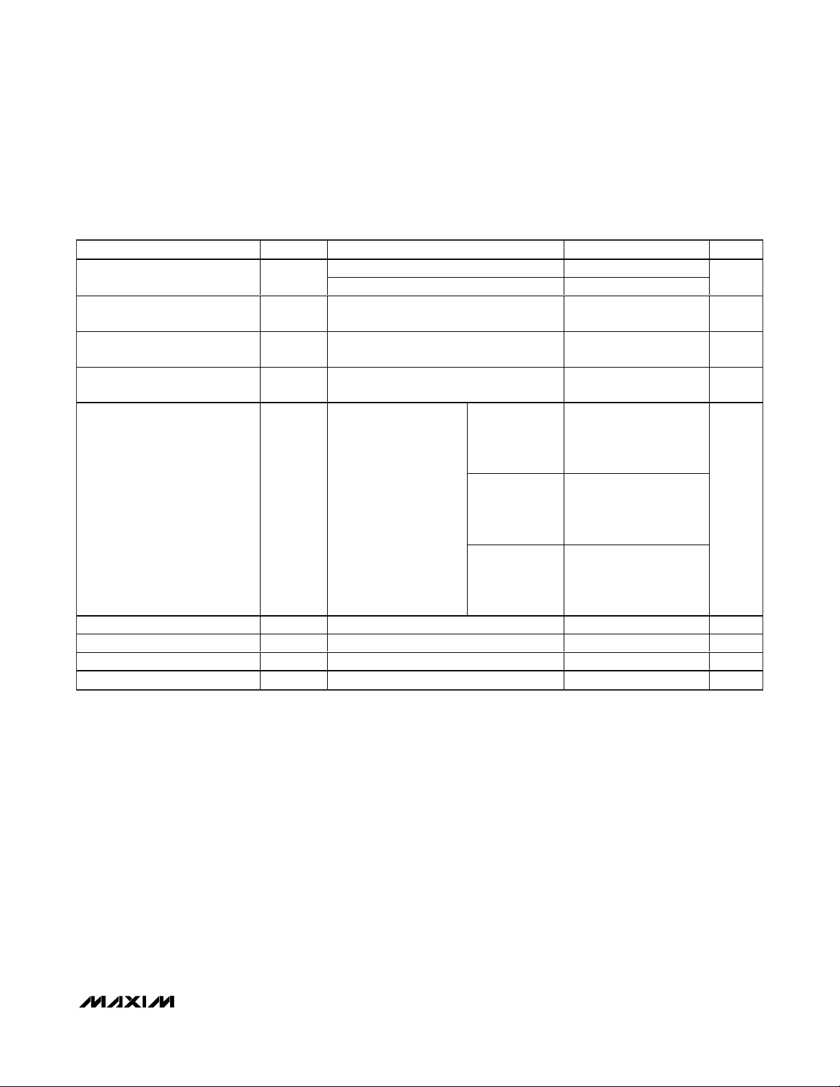
Pin Description
PIN NAME FUNCTION
1, 6, 8, 14 V
2RF
3, 4, 5, 10,
12, 13, 17
7 LOBIAS
9, 15 N.C. Not internally connected. Pins can be grounded.
11 LO
16 LEXT
18, 19 IF-, IF+
20 IFBIAS
—EP
CC
GND
Power Supply. Bypass to GND with 0.01µF capacitors as close as possible to the pin.
Single-Ended 50Ω RF Input. Internally matched and DC shorted to GND through a balun. Requires
an input DC-blocking capacitor.
Ground. Internally connected to the exposed pad. Connect all ground pins and the exposed pad
(EP) together.
LO Amplifier Bias Control. Output bias resistor for the LO buffer. Connect a 604Ω 1% resistor
(230mA bias condition) from LOBIAS to ground.
Local Oscillator Input. This input is internally matched to 50Ω. Requires an input DC-blocking
capacitor.
External Inductor Connection. Connect an inductor from this pin to ground to increase the RF-to-IF
and LO-to-IF isolation (see the Typical Operating Characteristics for typical performance vs. inductor
value).
Mixer Differential IF Output. Connect pullup inductors from each of these pins to V
Typical Application Circuit).
IF Amplifier Bias Control. IF bias resistor connection for the IF amplifier. Connect a 698Ω 1% resistor
(230mA bias condition) from IFBIAS to GND.
Exposed Pad. Internally connected to GND. Connect to a large ground plane using multiple vias to
maximize thermal and RF performance.
(see the
CC
Page 16

MAX19996
SiGe High-Linearity, 2000MHz to 3000MHz
Downconversion Mixer with LO Buffer
16 ______________________________________________________________________________________
Detailed Description
The MAX19996 high-linearity downconversion mixer
provides 8.7dB of conversion gain and +24.5dBm of
IIP3, with a typical 9.6dB noise figure. The integrated
baluns and matching circuitry allow for 50Ω singleended interfaces to the RF and the LO port. The integrated LO buffer provides a high drive level to the
mixer core, reducing the LO drive required at the
MAX19996’s input to a -3dBm to +3dBm range. The IF
port incorporates a differential output, which is ideal for
providing enhanced 2RF-2LO performance.
Specifications are guaranteed over broad frequency
ranges to allow for use in WCS, LTE, WiMAX, and
MMDS base stations. The MAX19996 is specified to
operate over an RF input range of 2000MHz to
3000MHz, an LO range of 1800MHz to 2550MHz, and
an IF range of 50MHz to 500MHz. The external IF components set the lower frequency range (see the
Typical
Operating Characteristics
for details). Operation
beyond these ranges is possible (see the
Typical
Operating Characteristics
for additional information).
Although this device is optimized for low-side LO injection applications, it can operate in high-side LO injection modes as well. However, performance degrades
as f
LO
continues to increase. For increased high-side
LO performance, refer to the MAX19996A data sheet.
RF Port and Balun
The MAX19996 RF input provides a 50Ω match when
combined with a series 8.2pF DC-blocking capacitor.
This DC-blocking capacitor is required as the input is
internally DC shorted to ground through the on-chip
balun. The RF port input return loss is typically 15dB
over the RF frequency range of 2300MHz to 2800MHz.
LO Inputs, Buffer, and Balun
The MAX19996 is optimized for low-side LO injection
applications with an 1800MHz to 2550MHz LO frequency range. The LO input is internally matched to 50Ω,
requiring only a 2pF DC-blocking capacitor. A twostage internal LO buffer allows for a -3dBm to +3dBm
LO input power range. The on-chip low-loss balun,
along with an LO buffer, drives the double-balanced
mixer. All interfacing and matching components from
the LO inputs to the IF outputs are integrated on-chip.
High-Linearity Mixer
The core of the MAX19996 is a double-balanced, highperformance passive mixer. Exceptional linearity is provided by the large LO swing from the on-chip LO
buffer. When combined with the integrated IF amplifiers, the performance of IIP3, 2RF-2LO rejection, and
noise-figure is typically +24.5dBm, 69dBc, and 9.6dB,
respectively.
Differential IF Output Amplifier
The MAX19996 has an IF frequency range of 50MHz to
500MHz, where the low-end frequency depends on the
frequency response of the external IF components. The
MAX19996 mixer is tuned for a 450MHz IF using 120nH
external pullup bias inductors. Lower IFs of 350MHz
and 300MHz require higher inductor values of 270nH
and 470nH, respectively. The differential, open-collector IF output ports require these inductors to be connected to V
CC
.
Note that these differential ports are ideal for providing
enhanced 2RF-2LO performance. Single-ended IF
applications require a 4:1 (impedance ratio) balun to
transform the 200Ω differential IF impedance to a 50Ω
single-ended system. Use the TC4-1W-17 4:1 transformer for IF frequencies above 200MHz and the
TC4-1W-7A 4:1 transformer for frequencies below
200MHz. The user can use a differential IF amplifier or
SAW filter on the mixer IF port, but a DC block is
required on both IF+/IF- ports to keep external DC from
entering the IF ports of the mixer.
Applications Information
Input and Output Matching
The RF and LO ports are designed to operate in a
50Ω system. Use DC blocks at the RF and LO inputs to
isolate the ports from external DC while providing some
reactive tuning. The IF output impedance is 200Ω (dif-
ferential). For evaluation, an external low-loss 4:1
(impedance-ratio) balun transforms this impedance
down to a 50Ω single-ended output (see the
Typical
Application Circuit
).
Externally Adjustable Bias
Bias currents for the LO buffer and the IF amplifier are
optimized by fine-tuning resistors R1 and R2. The values for R1 and R2, as listed in Table 1, represent the
nominal values which yield the highest level of linearity
performance. Larger value resistors can be used to
reduce power dissipation at the expense of some performance loss. Contact the factory for details concerning recommended power reduction vs. performance
tradeoffs. If ±1% resistors are not readily available,
±5% resistors can be substituted.
Significant reductions in power consumption can also be
realized by operating the mixer with an optional supply
voltage of +3.3V. Doing so reduces the overall power
consumption by up to 57%. See the
+3.3V Supply AC
Electrical Characteristics
table and the relevant +3.3V
curves in the
Typical Operating Characteristics
section
to evaluate the power vs. performance tradeoffs.
Page 17

MAX19996
LEXT Inductor
Short LEXT to ground using a 0Ω resistor. For applications requiring improved RF-to-IF and LO-to-IF isolation,
a 4.7nH low-ESR inductor can be connected from LEXT
to GND. However, the load impedance presented to the
mixer must be such that any capacitances from IF- and
IF+ to ground do not exceed several picofarads to
ensure stable operating conditions. Since approximately 120mA flows through LEXT, it is important to use a
low-DCR wire-wound inductor.
Layout Considerations
A properly designed PCB is an essential part of any
RF/microwave circuit. Keep RF signal lines as short as
possible to reduce losses, radiation, and inductance.
The load impedance presented to the mixer must be
such that any capacitance from both IF- and IF+ to
ground does not exceed several picofarads. For the best
performance, route the ground pin traces directly to the
exposed pad under the package. The PCB exposed pad
MUST be connected to the ground plane of the PCB. It is
suggested that multiple vias be used to connect this pad
to the lower-level ground planes. This method provides a
good RF/thermal-conduction path for the device. Solder
the exposed pad on the bottom of the device package to
the PCB. The MAX19996 evaluation kit can be used as a
reference for board layout. Gerber files are available
upon request at www.maxim-ic.com.
Power-Supply Bypassing
Proper voltage-supply bypassing is essential for highfrequency circuit stability. Bypass each VCCpin with
the capacitors shown in the
Typical Application Circuit
and see Table 1.
Exposed Pad RF/Thermal Considerations
The exposed pad (EP) of the MAX19996’s 20-pin thin
QFN package provides a low thermal-resistance path
to the die. It is important that the PCB on which the
MAX19996 is mounted be designed to conduct heat
from the EP. In addition, provide the EP with a lowinductance path to electrical ground. The EP MUST be
soldered to a ground plane on the PCB, either directly
or through an array of plated via holes.
Table 1. Component Values
*
Use 470nH inductors and TC4-1W-7A 4:1 balun for IF frequencies below 200MHz.
SiGe High-Linearity, 2000MHz to 3000MHz
Downconversion Mixer with LO Buffer
______________________________________________________________________________________ 17
DESIGNATION QTY DESCRIPTION COMPONENT SUPPLIER
C1 1 8.2pF microwave capacitor (0402) Murata Electronics North America, Inc.
C2, C6, C8, C11 4 0.01µF microwave capacitors (0402) Murata Electronics North America, Inc.
C3, C9 0 Not installed, capacitors —
C10 1 2pF microwave capacitor (0402) Murata Electronics North America, Inc.
C13, C14 2 1000pF microwave capacitors (0402) Murata Electronics North America, Inc.
C15 1 82pF microwave capacitor (0402) Murata Electronics North America, Inc.
L1, L2 2
L3 1 4.7nH wire-wound high-Q inductor (0603) Coilcraft, Inc.
R1 1
R2 1
R3 1 0Ω resistor (1206) Digi-Key Corp.
T1 1 4:1 IF balun TC4-1W-17* Mini-Circuits
U1 1 MAX19996 IC (20 TQFN) Maxim Integrated Products, Inc.
120nH wire-wound high-Q inductors* (0805)
(see the Typical Operating Characteristics)
698Ω ± 1% r esi stor ( 0402) . U se for V
1.1kΩ ± 1% r esi stor ( 0402) . U se for V
604Ω ± 1% r esi stor ( 0402) . U se for V
845Ω ± 1% r esi stor ( 0402) . U se for V
= +5 .0 V ap p l i cati ons.
C C
= +3 .3 V ap p l i cati ons.
C C
= +5 .0 V ap p l i cati ons.
C C
= +3 .3 V ap p l i cati ons.
C C
Coilcraft, Inc.
Digi-Key Corp.
Digi-Key Corp.
Page 18

MAX19996
SiGe High-Linearity, 2000MHz to 3000MHz
Downconversion Mixer with LO Buffer
18 ______________________________________________________________________________________
Typical Application Circuit
R3
C3 C2
RF
INPUT
C13
C14
+5.0V
C1
V
GND
GND
GND
IF-
C15
GND
MAX19996
326
T1
14
4:1
LEXT
16
IF
OUTPUT
L3
N.C.
15
V
CC
14
GND
13
GND
12
C10
LO
11
C11
+5.0V
LO
INPUT
L1
L2
R1
IF+
IFBIAS
1920 18 17
CC
1
RF
2
3
4
EP
5
+5.0V
768
LOBIAS
CC
V
C8
C9
N.C.
+5.0V
CC
V
C6
R2
10
9
GND
NOTE: PINS 3, 4, 5, 10, 12, 13, AND 17 ARE ALL INTERNAL LY
CONNECTED TO THE EXPOSED GROUND PAD. CONNECT
THESE PINS TO GROUND TO IMPROVE ISOLATION.
PINS 9 AND 15 HAVE NO INTERNAL CONNECTION BUT CAN BE
EXTERNALLY GROUNDED TO IMPROVE ISOLATION.
Page 19

MAX19996
SiGe High-Linearity, 2000MHz to 3000MHz
Downconversion Mixer with LO Buffer
Maxim cannot assume responsibility for use of any circuitry other than circuitry entirely embodied in a Maxim product. No circuit patent licenses are
implied. Maxim reserves the right to change the circuitry and specifications without notice at any time.
Maxim Integrated Products, 120 San Gabriel Drive, Sunnyvale, CA 94086 408-737-7600 ____________________
19
© 2008 Maxim Integrated Products is a registered trademark of Maxim Integrated Products, Inc.
Package Information
For the latest package outline information and land patterns, go
to www.maxim-ic.com/packages
.
PACKAGE TYPE PACKAGE CODE DOCUMENT NO.
20 Thin QFN-EP T2055-3
21-0140
MAX19996
TOP VIEW
1920 18 17
768
RF
GND
GND
9
V
CC
1
2
4
5
15
14
12
11
LOBIAS
V
CC
N.C.
GND
GND
3
13
16
10
V
CC
V
CC
GND
GND
LO
N.C.
IF+
IF-
GND
LEXT
IFBIAS
EP
Pin Configuration
Chip Information
PROCESS: SiGe BiCMOS
 Loading...