

Page 1
________________General Description
The MAX1668/MAX1805/MAX1989 are precise multichannel digital thermometers that report the temperature of all remote sensors and their own packages. The
remote sensors are diode-connected transistors—typically low-cost, easily mounted 2N3904 NPN types—that
replace conventional thermistors or thermocouples.
Remote accuracy is ±3°C for multiple transistor manufacturers, with no calibration needed. The remote channels can also measure the die temperature of other ICs,
such as microprocessors, that contain an on-chip,
diode-connected transistor.
The 2-wire serial interface accepts standard system
management bus (SMBus™) write byte, read byte, send
byte, and receive byte commands to program the alarm
thresholds and to read temperature data. The data format is 7 bits plus sign, with each bit corresponding to
1°C, in two’s-complement format.
The MAX1668/MAX1805/MAX1989 are available in
small, 16-pin QSOP surface-mount packages.
________________________Applications
____________________________Features
♦ Multichannel
4 Remote, 1 Local (MAX1668/MAX1989)
2 Remote, 1 Local (MAX1805)
♦ No Calibration Required
♦ SMBus 2-Wire Serial Interface
♦ Programmable Under/Overtemperature Alarms
♦ Supports SMBus Alert Response
♦ Accuracy
±2°C (+60°C to +100°C, Local)
±3°C (-40°C to +125°C, Local)
±3°C (+60°C to +100°C, Remote)
♦ 3µA (typ) Standby Supply Current
♦ 700µA (max) Supply Current
♦ Small, 16-Pin QSOP Package
MAX1668/MAX1805/MAX1989
†
Multichannel Remote/Local
Temperature Sensors
________________________________________________________________ Maxim Integrated Products 1
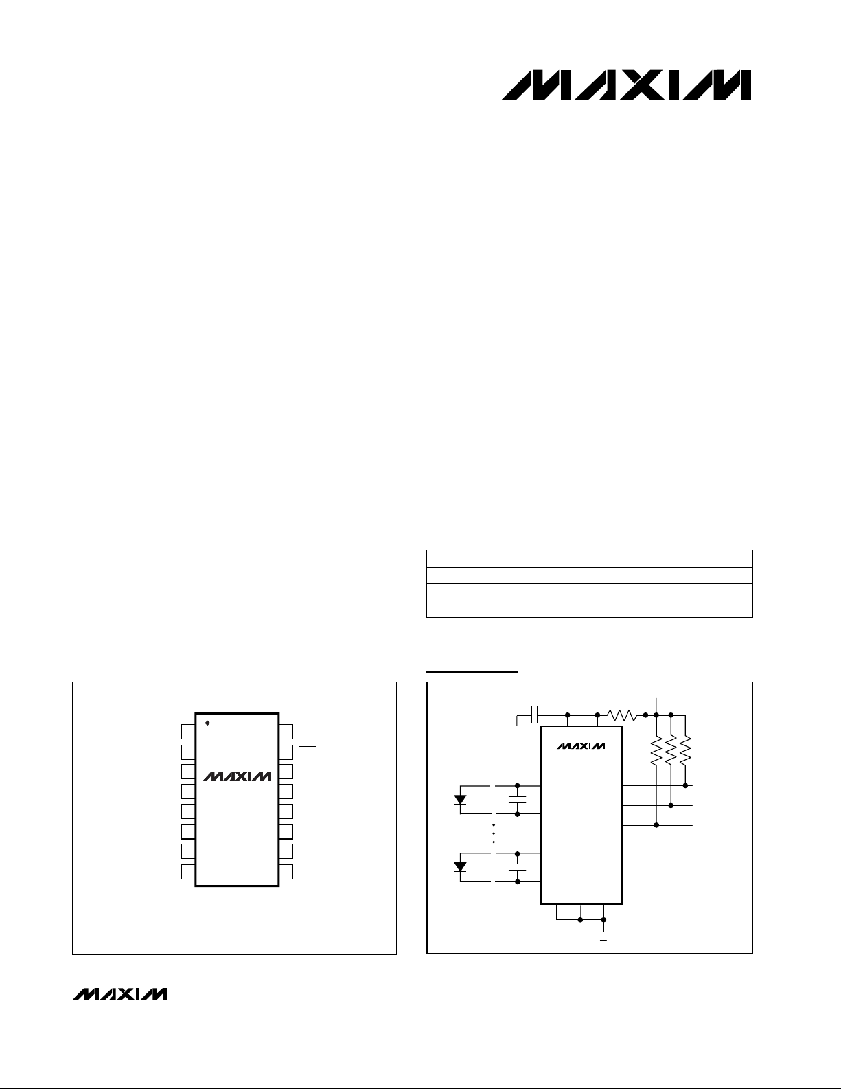
Pin Configuration
16
15
14
13
12
11
10
9
1
2
3
4
5
6
7
8
DXP1 GND
STBY
SMBCLK
SMBDATA
ALERT
ADD0
ADD1
V
CC
TOP VIEW
MAX1668
MAX1805
MAX1989
QSOP
DXN1
DXP2
(N.C.) DXN3
DXN2
(N.C.) DXP3
(N.C.) DXP4
( ) ARE FOR MAX1805.
(N.C.) DXN4
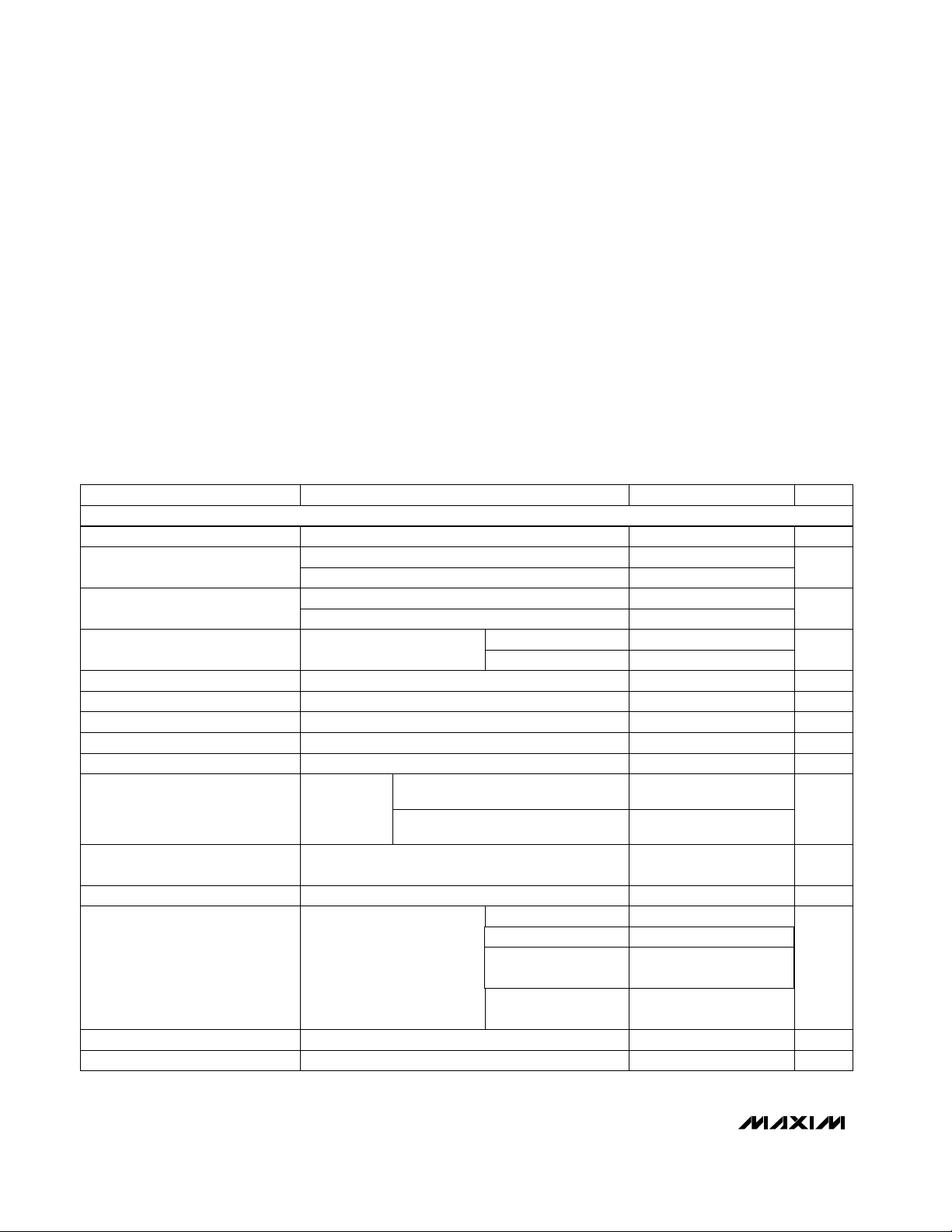
Typical Operating Circuit
19-1766; Rev 1; 8/02
PART
MAX1668MEE
-55°C to +125°C
TEMP RANGE PIN-PACKAGE
16 QSOP
_______________Ordering Information
SMBus is a trademark of Intel Corp. †Patents Pending
MAX1805MEE
-55°C to +125°C 16 QSOP
Desktop and Notebook
Computers
LAN Servers
Industrial Controls
Central-Office Telecom
Equipment
Test and Measurement
Multichip Modules
MAX1989MEE
-55°C to +125°C 16 QSOP
For pricing, delivery, and ordering information, please contact Maxim/Dallas Direct! at
1-888-629-4642, or visit Maxim’s website at www.maxim-ic.com.
*
*
*
DIODE-CONNECTED TRANSISTOR
0.1µF
V
STBY
CC
MAX1668
MAX1805
MAX1989
2200pF
DXP1
DXN1
DXP4
2200pF
DXN4
ADD0 ADD1
SMBCLK
SMBDATA
ALERT
GND
3V TO 5.5V
200Ω
10kΩ EACH
CLOCK
DATA
INTERRUPT
TO µC
Page 2
MAX1668/MAX1805/MAX1989
†
Multichannel Remote/Local
Temperature Sensors
2 _______________________________________________________________________________________
ABSOLUTE MAXIMUM RATINGS
ELECTRICAL CHARACTERISTICS
(VCC= +3.3V, STBY = VCC, configuration byte = X0XXXX00, TA= 0°C to +125°C, unless otherwise noted.)
Stresses beyond those listed under “Absolute Maximum Ratings” may cause permanent damage to the device. These are stress ratings only, and functional
operation of the device at these or any other conditions beyond those indicated in the operational sections of the specifications is not implied. Exposure to
absolute maximum rating conditions for extended periods may affect device reliability.
VCCto GND..............................................................-0.3V to +6V
DXP_, ADD_, STBY to GND........................-0.3V to (V
CC
+ 0.3V)
DXN_ to GND ........................................................-0.3V to +0.8V
SMBCLK, SMBDATA, ALERT to GND ......................-0.3V to +6V
SMBDATA, ALERT Current .................................-1mA to +50mA
DXN_ Current......................................................................±1mA
Continuous Power Dissipation (T
A
= +70°C)
QSOP (derate 8.30mW/°C above +70°C)....................667mW
Operating Temperature Range .........................-55°C to +125°C
Junction Temperature......................................................+150°C
Storage Temperature Range .............................-65°C to +150°C
Lead Temperature (soldering, 10s) .................................+300°C
DXP_ forced to 1.5VRemote-Diode Source Current
Low level (POR state)
Configuration byte =
X0XXXX10, high level
Configuration byte =
X0XXXX01, high level
High level (POR state)
71013
200
50
DXN_ Source Voltage 0.7 V
Hardware or software standby,
SMBCLK at 10kHz
SMBus static
TA = 0°C to +85°C
TA = +60°C to +100°C
Average measured over 4s; logic inputs forced
V
CC
or GND
Temperature Error, Local Diode
(Notes 1, 2)
-3.5 +3.5
°C
-2.5 +2.5
Including long-term drift
Temperature Error, Remote Diode
(Notes 2, 3)
-5 +5
°C
-3 +3
TR = -55°C to +125°C
TR = +60°C to +100°C
PARAMETER MIN TYP MAX UNITS
Undervoltage Lockout Hysteresis 50 mV
Undervoltage Lockout Threshold 2.60 2.8 2.95 V
Supply Voltage Range 3.0 5.5 V
Initial Temperature Error,
Local Diode (Note 2)
-3 +3
°C
Power-On Reset (POR) Threshold 1.3 1.8 2.3 V
POR Threshold Hysteresis 50 mV
310
Standby Supply Current
512
µA
Temperature Resolution (Note 1) 8 Bits
-2 +2
Average Operating Supply Current 400 700 µA
Conversion Time 260 320 380 ms
70 100 130
µA
Address Pin Bias Current 160 µA
CONDITIONS
VCCinput, disables A/D conversion, rising edge
TA = 0°C to +125°C
VCC, falling edge
From stop bit to conversion complete (all channels)
Logic inputs
forced to V
CC
or GND
ADD0, ADD1; momentary upon power-on reset
Monotonicity guaranteed
TA = +60°C to +100°C
ADC AND POWER SUPPLY
Page 3
MAX1668/MAX1805/MAX1989
†
Multichannel Remote/Local
Temperature Sensors
_______________________________________________________________________________________ 3
ELECTRICAL CHARACTERISTICS (continued)
(VCC= +3.3V, STBY = VCC, configuration byte = X0XXXX00, TA= 0°C to +125°C, unless otherwise noted.)
STBY, SMBCLK, SMBDATA; V
CC
= 3V to 5.5V
t
HIGH
, 90% to 90% points
t
LOW
, 10% to 10% points
(Note 4)
SMBCLK, SMBDATA
Logic inputs forced to VCCor GND
ALERT forced to 5.5V
STBY, SMBCLK, SMBDATA; VCC= 3V to 5.5V
ALERT, SMBDATA forced to 0.4V
CONDITIONS
µs4SMBCLK Clock High Time
µs4.7SMBCLK Clock Low Time
kHzDC 100SMBus Clock Frequency
pF5SMBus Input Capacitance
µA-1 +1Logic Input Current
µA1
ALERT Output High Leakage
Current
V2.2Logic Input High Voltage
V0.8Logic Input Low Voltage
mA6Logic Output Low Sink Current
UNITSMIN TYP MAXPARAMETER
t
SU:DAT
, 10% or 90% of SMBDATA to 10% of SMBCLK
t
SU:STO
, 90% of SMBCLK to 10% of SMBDATA
t
HD:STA
, 10% of SMBDATA to 90% of SMBCLK
t
SU:STA
, 90% to 90% points
ns250
SMBus Data Valid to SMBCLK
Rising-Edge Time
µs4SMBus Stop-Condition Setup Time
µs4SMBus Start-Condition Hold Time
ns250
SMBus Repeated Start-Condition
Setup Time
µs4.7SMBus Start-Condition Setup Time
nsSMBus Data-Hold Time
Master clocking in data µs1
SMBCLK Falling Edge to SMBus
Data-Valid Time
SMBus INTERFACE
ELECTRICAL CHARACTERISTICS
(VCC= +5V, STBY = VCC, configuration byte = X0XXXX00, TA= -55°C to +125°C, unless otherwise noted.) (Note 6)
CONDITIONS
Monotonicity guaranteed
TA= +60°C to +100°C
Bits8Temperature Resolution
-2 +2
TR= +60°C to +100°C
TA= -55°C to +125°C
°C
-3 +3
Initial Temperature Error,
Local Diode (Note 2)
V4.5 5.5Supply-Voltage Range
From stop bit to conversion complete (both channels) ms260 380Conversion Time
-3 +3
TR= -55°C to +125°C
°C
UNITSMIN TYP MAX
-5 +5
PARAMETER
Temperature Error, Remote Diode
(Notes 2, 3)
ADC AND POWER SUPPLY
t
HD:DAT
, slave receive (Note 5) 0
Page 4
0
8
4
16
12
20
24
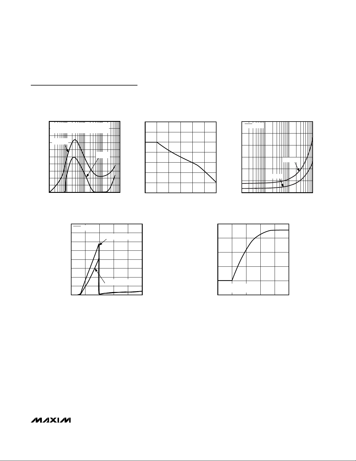
MAX1668/1805 toc03
FREQUENCY (MHz)
TEMPERATURE ERROR (°C)
TEMPERATURE ERROR
vs. SUPPLY NOISE FREQUENCY
100mV
P-P
0.1 1 10 100
WITH VCC 0.1µF CAPACITOR REMOVED
2200pF BETWEEN DXN_ AND DXP_
250mV
P-P
20
-20
1 10 100
TEMPERATURE ERROR
vs. PC BOARD RESISTANCE
-10
MAX1668/1805 toc01
LEAKAGE RESISTANCE (MΩ)
TEMPERATURE ERROR (°C)
0
10
PATH = DXP_ TO GND
PATH = DXP_ TO V
CC
(5V)
-2
-1
0
1
2
3
4
-50 -10-30 10 30 50 70 90 110
TEMPERATURE ERROR
vs. TEMPERATURE
MAX1668/1805 toc02
TEMPERATURE (°C)
TEMPERATURE ERROR (°C)
NPN (CMPT3904)
PNP (CMPT3906)
INTERNAL
Typical Operating Characteristics
(Typical Operating Circuit, VCC= +5V, STBY = VCC, configuration byte = X0XXXX00, TA = +25°C, unless otherwise noted.)
MAX1668/MAX1805/MAX1989
†
Multichannel Remote/Local
Temperature Sensors
4 _______________________________________________________________________________________
ELECTRICAL CHARACTERISTICS (continued)
(VCC= +5V, STBY = VCC, configuration byte = X0XXXX00, TA= -55°C to +125°C, unless otherwise noted.) (Note 6)
Note 1: Guaranteed by design, but not production tested.
Note 2: Quantization error is not included in specifications for temperature accuracy. For example, if the MAX1668/MAX1805/
MAX1989 device temperature is exactly +66.7°C, the ADC may report +66°C, +67°C, or +68°C (due to the quantization
error plus the +0.5°C offset used for rounding up) and still be within the guaranteed ±1°C error limits for the +60°C to
+100°C temperature range. See Table 2.
Note 3: A remote diode is any diode-connected transistor from Table 1. T
R
is the junction temperature of the remote diode. See the
Remote-Diode Selection section for remote-diode forward-voltage requirements.
Note 4: The SMBus logic block is a static design that works with clock frequencies down to DC. While slow operation is possible, it
violates the 10kHz minimum clock frequency and SMBus specifications, and can monopolize the bus.
Note 5: Note that a transition must internally provide at least a hold time in order to bridge the undefined region (300ns max) of
SMBCLK’s falling edge t
HD:DAT.
Note 6: Specifications from -55°C to +125°C are guaranteed by design, not production tested.
CONDITIONS UNITSMIN TYP MAXPARAMETER
STBY, SMBCLK, SMBDATA; VCC= 4.5V to 5.5V
Logic Input High Voltage V2.4
ALERT forced to 5.5V
µA1
ALERT Output High Leakage
Current
Logic inputs forced to VCCor GND µA-2 +2Logic Input Current
ALERT, SMBDATA forced to 0.4V
mA6Logic Output Low Sink Current
STBY, SMBCLK, SMBDATA; VCC= 4.5V to 5.5V
V0.8Logic Input Low Voltage
SMBus INTERFACE
Page 5
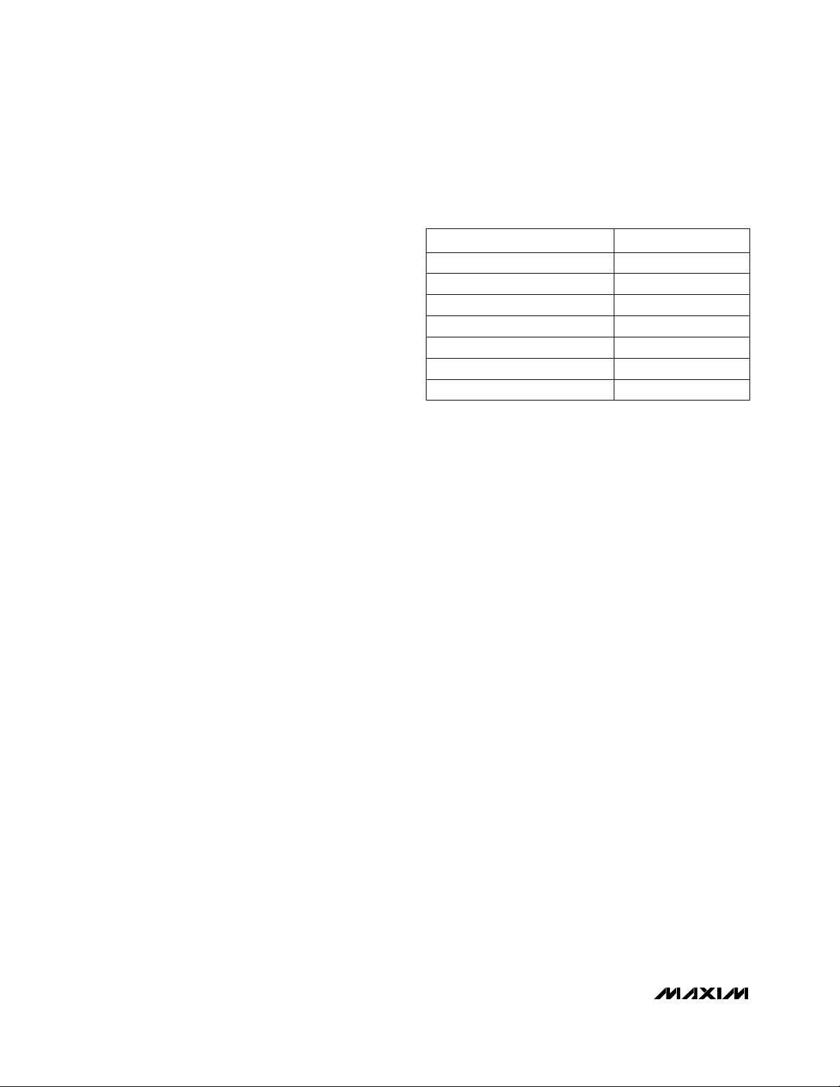
0
20
40
60
80
100
120
140
160
012345
STANDBY SUPPLY CURRENT
vs. SUPPLY VOLTAGE
MAX1668/1805 toc07
SUPPLY VOLTAGE (V)
SUPPLY CURRENT (µA)
STBY = GND
ADD0 = ADD1 = HIGH-Z
ADD0 = ADD1 = GND
0
25
75
50
100
125
-2 20468
RESPONSE TO THERMAL SHOCK
MAX1668/1805 toc08
TIME (s)
TEMPERATURE (°C)
16 QSOP IMMERSED IN
+115°C FLUORINERT BATH
MAX1668/MAX1805/MAX1989
†
Multichannel Remote/Local
Temperature Sensors
_______________________________________________________________________________________ 5
Typical Operating Characteristics (continued)
(Typical Operating Circuit, VCC= +5V, STBY = VCC, configuration byte = X0XXXX00, TA = +25°C, unless otherwise noted.)
TEMPERATURE ERROR
vs. DXP_ TO DXN_ CAPACITANCE
MAX16681805 toc05
DXP_ TO DXN_ CAPACITANCE (nF)
TEMPERATURE ERROR (°C)
-10
-6
-8
-2
-4
2
0
4
0203010 40 50 60
STANDBY SUPPLY CURRENT
vs. CLOCK FREQUENCY
MAX1668/1805 toc06
SMBCLK FREQUENCY (kHz)
SUPPLY CURRENT (µA)
60
0
10
20
30
40
50
1 10 100 1000
STBY = GND
VCC = 5V
VCC = 3.3V
TEMPERATURE ERROR
vs. COMMON-MODE NOISE FREQUENCY
2.0
SQUARE-WAVE AC-COUPLED INTO DXN
1.8
2200pF BETWEEN DXN_ AND DXP_
1.6
100mV
1.4
1.2
1.0
0.8
0.6
TEMPERATURE ERROR (°C)
0.4
0.2
0
P-P
0.1 1 1000
10 100
FREQUENCY (MHz)
50mV
P-P
MAX1668/1805 toc04
Page 6

MAX1668/MAX1805/MAX1989
†
Multichannel Remote/Local
Temperature Sensors
6 _______________________________________________________________________________________
_______________Detailed Description
The MAX1668/MAX1805/MAX1989 are temperature
sensors designed to work in conjunction with an external microcontroller (µC) or other intelligence in thermostatic, process-control, or monitoring applications. The
µC is typically a power-management or keyboard controller, generating SMBus serial commands by “bitbanging” general-purpose input-output (GPIO) pins or
through a dedicated SMBus interface block.
These devices are essentially 8-bit serial analog-to-digital converters (ADCs) with sophisticated front ends.
However, the MAX1668/MAX1805/MAX1989 also contain
a switched current source, a multiplexer, an ADC, an
SMBus interface, and associated control logic (Figure 1).
In the MAX1668 and MAX1989, temperature data from
the ADC is loaded into five data registers, where it is
automatically compared with data previously stored in
10 over/undertemperature alarm registers. In the
MAX1805, temperature data from the ADC is loaded into
three data registers, where it is automatically compared
with data previously stored in six over/undertemperature
alarm registers.
ADC and Multiplexer
The ADC is an averaging type that integrates over a
64ms period (each channel, typical), with excellent
noise rejection.
The multiplexer automatically steers bias currents
through the remote and local diodes, measures their
forward voltages, and computes their temperatures.
Each channel is automatically converted once the conversion process has started. If any one of the channels
is not used, the device still performs measurements on
these channels, and the user can ignore the results of
the unused channel. If any remote-diode channel is
unused, connect DXP_ to DXN_ rather than leaving the
pins open.
The DXN_ input is biased at 0.65V above ground by an
internal diode to set up the A/D inputs for a differential
measurement. The worst-case DXP_ to DXN_ differential
input voltage range is 0.25V to 0.95V.
Excess resistance in series with the remote diode causes about +0.5°C error per ohm. Likewise, 200µV of offset
voltage forced on DXP_ to DXN_ causes about 1°C error.
MAX1668/
MAX1989
FUNCTION
1, 3, 5, 7 DXP_
Combined Current Source and A/D Positive Input for Remote-Diode Channel. Do not
leave DXP floating; connect DXP to DXN if no remote diode is used. Place a 2200pF
capacitor between DXP and DXN for noise filtering.
PIN
12
ALERT
SMBus Alert (Interrupt) Output, Open Drain
11 ADD0 SMBus Slave Address Select Pin
10 ADD1
SMBus Address Select Pin (Table 8). ADD0 and ADD1 are sampled upon power-up.
Excess capacitance (>50pF) at the address pins when floating can cause addressrecognition problems.
15
STBY
Hardware Standby Input. Temperature and comparison threshold data are retained in
standby mode. Low = standby mode, high = operate mode.
14 SMBCLK SMBus Serial-Clock Input
13 SMBDATA SMBus Serial-Data Input/Output, Open Drain
1, 3
12
11
10
15
14
13
Pin Description
NAMEMAX1805
2, 4, 6, 8 DXN_
Combined Current Sink and A/D Negative Input. DXN is normally biased to a diode voltage above ground.
2, 4
9 V
CC
Supply Voltage Input, 3V to 5.5V. Bypass to GND with a 0.1µF capacitor. A 200Ω series
resistor is recommended but not required for additional noise filtering.
9
16 GND Ground16
—
N.C. No Connection. Not internally connected. Can be used for PC board trace routing.5–8
Page 7

MAX1668/MAX1805/MAX1989
†
Multichannel Remote/Local
Temperature Sensors
_______________________________________________________________________________________ 7
Figure 1. MAX1668/MAX1805/MAX1989 Functional Diagram
DXP4
DXP3
DXP2
DXP1
DXN4
DXN3
DXN2
DXN1
LOCAL
CURRENT
SOURCES
MUX
DIODE
FAULT
ADC
CONTROL
LOGIC
SMBus
ADDRESS
DECODER
STBY ADD ADD1
SMBDATA
SMBCLK
ALERT
Q
R
S
DIGITAL COMPARATORS
ALERT RESPONSE
CONFIGURATION BYTE
ADDRESS REGISTER
REGISTER
STATUS BYTE REGISTERS
1 AND 2
COMMAND BYTE REGISTER
TEMPERATURE DATA REGISTERS
HIGH LIMITS REGISTERS
LOW LIMITS REGISTERS
ALERT MASK
REGISTER
NOTE: DOTTED LINES ARE FOR MAX1668 AND MAX1989.
Page 8
A/D Conversion Sequence
If a start command is written (or generated automatically
in the free-running autoconvert mode), all channels are
converted, and the results of all measurements are
available after the end of conversion. A BUSY status bit
in the status byte shows that the device is actually performing a new conversion; however, even if the ADC is
busy, the results of the previous conversion are always
available.
Remote-Diode Selection
Temperature accuracy depends on having a good-quality, diode-connected small-signal transistor. Accuracy
has been experimentally verified for all of the devices
listed in Table 1. The MAX1668/MAX1805/MAX1989 can
also directly measure the die temperature of CPUs and
other ICs having on-board temperature-sensing diodes.
The transistor must be a small-signal type, either NPN
or PNP, with a relatively high forward voltage; otherwise, the A/D input voltage range can be violated. The
forward voltage must be greater than 0.25V at 10µA;
check to ensure this is true at the highest expected
temperature. The forward voltage must be less than
0.95V at 100µA; check to ensure this is true at the lowest expected temperature. Large power transistors do
not work at all. Also, ensure that the base resistance is
less than 100Ω. Tight specifications for forward-current
gain (+50 to +150, for example) indicate that the manufacturer has good process controls and that the
devices have consistent VBE characteristics.
For heat-sink mounting, the 500-32BT02-000 thermal
sensor from Fenwal Electronics is a good choice. This
device consists of a diode-connected transistor, an
aluminum plate with screw hole, and twisted-pair cable
(Fenwal Inc., Milford, MA, 508-478-6000).
Thermal Mass and Self-Heating
Thermal mass can seriously degrade the MAX1668/
MAX1805/MAX1989s’ effective accuracy. The thermal
time constant of the 16-pin QSOP package is about
140s in still air. For the MAX1668/MAX1805/MAX1989
junction temperature to settle to within +1°C after a
sudden +100°C change requires about five time constants or 12 minutes. The use of smaller packages for
remote sensors, such as SOT23s, improves the situation. Take care to account for thermal gradients
between the heat source and the sensor, and ensure
that stray air currents across the sensor package do
not interfere with measurement accuracy.
Self-heating does not significantly affect measurement
accuracy. Remote-sensor self-heating due to the diode
current source is negligible. For the local diode, the
worst-case error occurs when sinking maximum current
at the ALERT output. For example, with ALERT sinking
1mA, the typical power dissipation is VCCx 400µA plus
0.4V x 1mA. Package theta J-A is about 150°C/W, so
with VCC= 5V and no copper PC board heat sinking,
the resulting temperature rise is:
dT = 2.4mW x 150°C/W = 0.36°C
Even with these contrived circumstances, it is difficult
to introduce significant self-heating errors.
ADC Noise Filtering
The ADC is an integrating type with inherently good
noise rejection, especially of low-frequency signals such
as 60Hz/120Hz power-supply hum. Micropower operation places constraints on high-frequency noise rejection; therefore, careful PC board layout and proper
external noise filtering are required for high-accuracy
remote measurements in electrically noisy environments.
High-frequency EMI is best filtered at DXP_ and DXN_
with an external 2200pF capacitor. This value can be
increased to about 3300pF (max), including cable
capacitance. Higher capacitance than 3300pF introduces errors due to the rise time of the switched current source.
Nearly all noise sources tested cause additional error
measurements, typically by +1°C to +10°C, depending
on the frequency and amplitude (see the Typical
Operating Characteristics).
PC Board Layout
1) Place the MAX1668/MAX1805/MAX1989 as close as
practical to the remote diode. In a noisy environment,
such as a computer motherboard, this distance can
MAX1668/MAX1805/MAX1989
†
Multichannel Remote/Local
Temperature Sensors
8 _______________________________________________________________________________________
CMPT3904Central Semiconductor (USA)
MMBT3904Motorola (USA)
MMBT3904
SST3904Rohm Semiconductor (Japan)
KST3904-TFSamsung (Korea)
FMMT3904CT-NDZetex (England)
MANUFACTURER MODEL NO.
SMBT3904Siemens (Germany)
Table 1. Remote-Sensor Transistor
Manufacturers
Note: Transistors must be diode connected (base shorted to
collector).
National Semiconductor (USA)
Page 9

be 4in to 8in (typ) or more as long as the worst noise
sources (such as CRTs, clock generators, memory
buses, and ISA/PCI buses) are avoided.
2) Do not route the DXP_ to DXN_ lines next to the
deflection coils of a CRT. Also, do not route the
traces across a fast memory bus, which can easily
introduce +30°C error, even with good filtering.
Otherwise, most noise sources are fairly benign.
3) Route the DXP_ and DXN_ traces in parallel and in
close proximity to each other, away from any highvoltage traces such as +12VDC. Leakage currents
from PC board contamination must be dealt with
carefully, since a 20MΩ leakage path from DXP_ to
ground causes about +1°C error.
4) Connect guard traces to GND on either side of the
DXP_ to DXN_ traces (Figure 2). With guard traces
in place, routing near high-voltage traces is no
longer an issue.
5) Route through as few vias and crossunders as possible to minimize copper/solder thermocouple effects.
6) When introducing a thermocouple, make sure that
both the DXP_ and the DXN_ paths have matching
thermocouples. In general, PC board-induced thermocouples are not a serious problem. A copper-solder thermocouple exhibits 3µV/°C, and it takes
about 200µV of voltage error at DXP_ to DXN_ to
cause a +1°C measurement error. So, most parasitic thermocouple errors are swamped out.
7) Use wide traces. Narrow ones are more inductive
and tend to pick up radiated noise. The 10mil
widths and spacings recommended in Figure 2 are
not absolutely necessary (as they offer only a minor
improvement in leakage and noise), but try to use
them where practical.
8) Copper cannot be used as an EMI shield, and only
ferrous materials such as steel work well. Placing a
copper ground plane between the DXP_ to DXN_
traces and traces carrying high-frequency noise signals does not help reduce EMI.
PC Board Layout Checklist
• Place the MAX1668/MAX1805/MAX1989 as close as
possible to the remote diodes.
• Keep traces away from high voltages (+12V bus).
• Keep traces away from fast data buses and CRTs.
• Use recommended trace widths and spacings.
• Place a ground plane under the traces.
• Use guard traces flanking DXP_ and DXN_ and con-
necting to GND.
• Place the noise filter and the 0.1µF V
CC
bypass
capacitors close to the MAX1668/MAX1805/
MAX1989.
• Add a 200Ω resistor in series with V
CC
for best noise
filtering (see the Typical Operating Circuit).
Twisted-Pair and Shielded Cables
For remote-sensor distances longer than 8in, or in particularly noisy environments, a twisted pair is recommended. Its practical length is 6ft to 12ft (typ) before noise
becomes a problem, as tested in a noisy electronics laboratory. For longer distances, the best solution is a
shielded twisted pair like that used for audio microphones. For example, Belden #8451 works well for distances up to 100ft in a noisy environment. Connect the
twisted pair to DXP_ and DXN_ and the shield to GND,
and leave the shield’s remote end unterminated.
Excess capacitance at DX_ _ limits practical remote-sensor distances (see the Typical Operating Characteristics).
For very long cable runs, the cable’s parasitic capacitance often provides noise filtering, so the 2200pF capacitor can often be removed or reduced in value.
Cable resistance also affects remote-sensor accuracy;
1Ω series resistance introduces about +0.5°C error.
Low-Power Standby Mode
Standby mode disables the ADC and reduces the supply-current drain to less than 12µA. Enter standby
mode by forcing the STBY pin low or through the
RUN/STOP bit in the configuration byte register.
Hardware and software standby modes behave almost
identically: all data is retained in memory, and the SMB
interface is alive and listening for reads and writes.
Activate hardware standby mode by forcing the STBY
pin low. In a notebook computer, this line can be connected to the system SUSTAT# suspend-state signal.
The STBY pin low state overrides any software conversion
command. If a hardware or software standby command
is received while a conversion is in progress, the conver-
MAX1668/MAX1805/MAX1989
†
Multichannel Remote/Local
Temperature Sensors
_______________________________________________________________________________________ 9
Figure 2. Recommended DXP_/DXN_ PC Traces
GND
10mils
10mils
10mils
DXP_
DXN_
GND
MINIMUM
10mils
Page 10

sion cycle is truncated, and the data from that conversion
is not latched into either temperature-reading register. The
previous data is not changed and remains available.
In standby mode, supply current drops to about 3µA.
At very low supply voltages (under the power-on-reset
threshold), the supply current is higher due to the
address pin bias currents. It can be as high as 100µA,
depending on ADD0 and ADD1 settings.
SMBus Digital Interface
From a software perspective, the MAX1668/MAX1805/
MAX1989 appear as a set of byte-wide registers that
contain temperature data, alarm threshold values, or
control bits. A standard SMBus 2-wire serial interface is
used to read temperature data and write control bits and
alarm threshold data. Each A/D channel within the
devices responds to the same SMBus slave address for
normal reads and writes.
The MAX1668/MAX1805/MAX1989 employ four standard
SMBus protocols: write byte, read byte, send byte, and
receive byte (Figure 3). The shorter receive byte protocol
allows quicker transfers, provided that the correct data
register was previously selected by a read byte instruc-
tion. Use caution with the shorter protocols in multimaster
systems, since a second master could overwrite the command byte without informing the first master.
The temperature data format is 7 bits plus sign in two’s-complement form for each channel, with each data bit representing 1°C (Table 2), transmitted MSB first. Measurements are
offset by +0.5°C to minimize internal rounding errors; for
example, +99.6°C is reported as +100°C.
Alarm Threshold Registers
Ten (six for MAX1805) registers store alarm threshold
data, with high-temperature (T
HIGH
) and low-tempera-
ture (T
LOW
) registers for each A/D channel. If either
measured temperature equals or exceeds the corresponding alarm threshold value, an ALERT interrupt is
asserted.
The power-on-reset (POR) state of all T
HIGH
registers of
the MAX1668 and MAX1805 is full scale (0111 1111, or
+127°C). The POR state of the channel 1 T
HIGH
register
of the MAX1989 is 0110 1110 or +110°C, while all other
channels are at +127°C. The POR state of all T
LOW
reg-
isters is 1100 1001 or -55°C.
MAX1668/MAX1805/MAX1989
†
Multichannel Remote/Local
Temperature Sensors
10 ______________________________________________________________________________________
ACK
7 bits
ADDRESS ACKWR
8 bits
DATA ACK
1
P
8 bits
S COMMAND
Write Byte Format
Read Byte Format
Send Byte Format Receive Byte Format
Slave Address: equivalent to chip-select line of
a 3-wire interface
Command Byte: selects which
register you are writing to
Data Byte: data goes into the register
set by the command byte (to set
thresholds, configuration masks, and
sampling rate)
ACK
7 bits
ADDRESS ACKWR S ACK
8 bits
DATA
7 bits
ADDRESS RD
8 bits
/// PS COMMAND
Slave Address: equivalent to chip-select line
Command Byte: selects
which register you are
reading from
Slave Address: repeated
due to change in dataflow direction
Data Byte: reads from
the register set by the
command byte
ACK
7 bits
ADDRESS WR
8 bits
COMMAND ACK PS ACK
7 bits
ADDRESS RD
8 bits
DATA /// PS
Command Byte: sends command with no data
Data Byte: This command only
works immediately following a
Read Byte. Reads data from the
register commanded by that last
Read Byte; also used for SMBus
Alert Response return address
S = Start condition Shaded = Slave transmission
P = Stop condition /// = Not acknowledged
Figure 3. SMBus Protocols
Page 11

Diode Fault Alarm
There is a continuity fault detector at DXP_ that detects
whether the remote diode has an open-circuit condition. At the beginning of each conversion, the diode
fault is checked, and the status byte is updated. This
fault detector is a simple voltage detector; if DXP_ rises
above VCC- 1V (typ) due to the diode current source, a
fault is detected. Note that the diode fault is not
checked until a conversion is initiated, so immediately
after power-on reset, the status byte indicates no fault
is present, even if the diode path is broken.
If any remote channel is shorted (DXP_ to DXN_ or
DXP_ to GND), the ADC reads 0000 0000 so as not to
trip either the T
HIGH
or T
LOW
alarms at their POR settings. In applications that are never subjected to 0°C in
normal operation, a 0000 0000 result can be checked
to indicate a fault condition in which DXP_ is accidentally short circuited. Similarly, if DXP_ is short circuited
to VCC, the ADC reads +127°C for all remote and local
channels, and the device alarms.
AALLEERRTT
Interrupts
The ALERT interrupt output signal is latched and can
only be cleared by reading the alert response address.
Interrupts are generated in response to T
HIGH
and T
LOW
comparisons and when a remote diode is disconnected
(for continuity fault detection). The interrupt does not halt
automatic conversions; new temperature data continues
to be available over the SMBus interface after ALERT is
asserted. The interrupt output pin is open drain so that
devices can share a common interrupt line. The interrupt
rate can never exceed the conversion rate.
The interface responds to the SMBus alert response
address, an interrupt pointer return-address feature
(see Alert Response Address section). Prior to taking
corrective action, always check to ensure that an interrupt is valid by reading the current temperature.
Alert Response Address
The SMBus alert response interrupt pointer provides
quick fault identification for simple slave devices that
lack the complex, expensive logic needed to be a bus
master. Upon receiving an ALERT interrupt signal, the
host master can broadcast a receive byte transmission
to the alert response slave address (0001 100). Then
any slave device that generated an interrupt attempts
to identify itself by putting its own address on the bus
(Table 3).
The alert response can activate several different slave
devices simultaneously, similar to the I2C general call. If
more than one slave attempts to respond, bus arbitration rules apply, and the device with the lower address
code wins. The losing device does not generate an
acknowledge and continues to hold the ALERT line low
until serviced (implies that the host interrupt input is
MAX1668/MAX1805/MAX1989
†
Multichannel Remote/Local
Temperature Sensors
______________________________________________________________________________________ 11
Table 2. Data Format (Two’s Complement) Table 3. Read Format for Alert Response
Address (0001100)
ADD66
Provide the current
MAX1668/MAX1805/MAX1989
slave address that was latched at
POR (Table 8)
FUNCTION
ADD55
ADD44
ADD33
ADD22
ADD11
ADD7
7
(MSB)
1
0
(LSB)
Logic 1
BIT NAME
TEMP
(°C)
+130.00 +127 0 111 1111
+127.00 +127 0 111 1111
+126.50 +127 0 111 1111
+126.00 +126 0 111 1110
+25.25 +25 0 001 1001
+0.50 +1 0 000 0000
+0.25 +0 0 000 0000
+0.00 +0 0 000 0000
-0.25 +0 0 000 0000
-0.50 +0 0 000 0000
-0.75 -1 1 111 1111
-1.00 -1 1 111 1111
-25.00 -25 1 110 0111
-25.50 -25 1 110 0110
-54.75 -55 1 100 1001
-55.00 -55 1 100 1001
-65.00 -65 1 011 1111
-70.00 -65 1 011 1111
ROUNDED
TEMP
(°C)
DIGITAL OUTPUT DATA BITS
SIGN MSB LSB
Page 12

level sensitive). Successful reading of the alert
response address clears the interrupt latch.
Command Byte Functions
The 8-bit command byte register (Table 4) is the master
index that points to the various other registers within the
MAX1668/MAX1805/MAX1989. The register’s POR
state is 0000 0000, so that a receive byte transmission
(a protocol that lacks the command byte) that occurs
immediately after POR returns the current local temperature data.
MAX1668/MAX1805/MAX1989
†
Multichannel Remote/Local
Temperature Sensors
12 ______________________________________________________________________________________
Table 4. Command Byte Bit Assignments for MAX1668/MAX1805/MAX1989
*If the device is in hardware standby mode at POR, all temperature registers read 0°C.
**Not available for MAX1805.
REGISTER COMMAND POR STATE FUNCTION
RIT 00h 0000 0000* Read local temperature
RET1 01h 0000 0000* Read remote DX1 temperature
RET2 02h 0000 0000* Read remote DX2 temperature
RET3** 03h 0000 0000* Read remote DX3 temperature
RET4** 04h 0000 0000* Read remote DX4 temperature
RS1 05h 0000 0000 Read status byte 1
RS2 06h 0000 0000 Read status byte 2
RC 07h 0000 0000 Read Configuration Byte
RIHL 08h 0111 1111 Read local T
HIGH
limit
RILL 09h 1100 1001 Read local T
LOW
limit
REHL1 0Ah
0111 1111
(0110 1110)
Read remote DX1 T
HIGH
limit (MAX1989)
RELL1 0Bh 1100 1001 Read remote DX1 T
LOW
limit
REHL2 0Ch 0111 1111 Read remote DX2 T
HIGH
limit
RELL2 0Dh 1100 1001 Read remote DX2 T
LOW
limit
REHL3** 0Eh 0111 1111 Read remote DX3 T
HIGH
limit
RELL3** 0Fh 1100 1001 Read remote DX3 T
LOW
limit
REHL4** 10h 0111 1111 Read remote DX4 T
HIGH
limit
RELL4** 11h 1100 1001 Read remote DX4 T
LOW
limit
WC 12h N/A Write configuration byte
WIHL 13h N/A Write local T
HIGH
limit
WILL 14h N/A Write local T
LOW
limit
WEHI1 15h N/A Write remote DX1 T
HIGH
limit
WELL1 16h N/A Write remote DX1 T
LOW
limit
WEHI2 17h N/A Write remote DX2 T
HIGH
limit
WELL2 18h N/A Write remote DX2 T
LOW
limit
WEHI3** 19h N/A Write remote DX3 T
HIGH
limit
WELL3** 1Ah N/A Write remote DX3 T
LOW
limit
WEHI4** 1Bh N/A Write remote DX4 T
HIGH
limit
WELL4** 1Ch N/A Write remote DX4 T
LOW
limit
MFG ID FEh 0100 1101 Read manufacture ID
DEV ID FFh
0000 0011 (0000 0101)
[0000 1011]
Read device ID (for MAX1805) [for MAX1989]
Page 13

MAX1668/MAX1805/MAX1989
†
Multichannel Remote/Local
Temperature Sensors
______________________________________________________________________________________ 13
Manufacturer and Device
ID Codes
Two ROM registers provide manufacturer and device
ID codes. Reading the manufacturer ID returns 4Dh,
which is the ASCII code M (for Maxim). Reading the
device ID returns 03h for MAX1668, 05h for MAX1805,
and 0Bh for MAX1989. If the read word 16-bit SMBus
protocol is employed (rather than the 8-bit Read Byte),
the least significant byte contains the data and the most
significant byte contains 00h in both cases.
Configuration Byte Functions
The configuration byte register (Table 5) is used to
mask (disable) interrupts and to put the device in software standby mode.
Status Byte Functions
The two status byte registers (Tables 6 and 7) indicate
which (if any) temperature thresholds have been
exceeded. The first byte also indicates whether the
ADC is converting and whether there is an open circuit
in a remote-diode DXP_ to DXN_ path. After POR, the
normal state of all the flag bits is zero, assuming none
of the alarm conditions are present. The status byte is
cleared by any successful read of the status byte,
unless the fault persists. Note that the ALERT interrupt
latch is not automatically cleared when the status flag
bit is cleared.
When reading the status byte, you must check for internal bus collisions caused by asynchronous ADC timing,
or else disable the ADC prior to reading the status byte
(through the RUN/STOP bit in the configuration byte).
To check for internal bus collisions, read the status
byte. If the least significant 7 bits are ones, discard the
data and read the status byte again. The status bits
LHIGH, LLOW, RHIGH, and RLOW are refreshed on the
SMBus clock edge immediately following the stop condition, so there is no danger of losing temperature-related status data as a result of an internal bus collision.
The OPEN status bit (diode continuity fault) is only
refreshed at the beginning of a conversion, so OPEN
data is lost. The ALERT interrupt latch is independent of
the status byte register, so no false alerts are generated
by an internal bus collision.
If the THIGH and TLOW limits are close together, it’s
possible for both high-temp and low-temp status bits to
be set, depending on the amount of time between status read operations (especially when converting at the
fastest rate). In these circumstances, it’s best not to rely
on the status bits to indicate reversals in long-term tem-
perature changes and instead use a current temperature reading to establish the trend direction.
Conversion Rate
The MAX1668/MAX1805/MAX1989 are continuously
measuring temperature on each channel. The typical
conversion rate is approximately three conversions/s
(for both devices). The resulting data is stored in the
temperature data registers.
Slave Addresses
The MAX1668/MAX1805/MAX1989 appear to the
SMBus as one device having a common address for all
ADC channels. The device address can be set to one
of nine different values by pin-strapping ADD0 and
ADD1 so that more than one MAX1668/MAX1805/
MAX1989 can reside on the same bus without address
conflicts (Table 8).
The address pin states are checked at POR only, and
the address data stays latched to reduce quiescent
supply current due to the bias current needed for high-Z
state detection.
The MAX1668/MAX1805/MAX1989 also respond to the
SMBus alert response slave address (see the Alert
Response Address section).
POR and Undervoltage Lockout
The MAX1668/MAX1805/MAX1989 have a volatile
memory. To prevent ambiguous power-supply conditions from corrupting the data in memory and causing
erratic behavior, a POR voltage detector monitors V
CC
and clears the memory if VCCfalls below 1.8V (typ, see
the Electrical Characteristics table). When power is first
applied and V
CC
rises above 1.85V (typ), the logic
blocks begin operating, although reads and writes at
V
CC
levels below 3V are not recommended. A second
V
CC
comparator, the ADC UVLO comparator, prevents
the ADC from converting until there is sufficient headroom (VCC= 2.8V typ).
Power-Up Defaults
• Interrupt latch is cleared.
• Address select pins are sampled.
• ADC begins converting.
• Command byte is set to 00h to facilitate quick
remote receive byte queries.
• T
HIGH
and T
LOW
registers are set to max and min
limits, respectively.
Page 14
MAX1668/MAX1805/MAX1989
†
Multichannel Remote/Local
Temperature Sensors
14 ______________________________________________________________________________________
Table 5. Configuration Byte Bit Assignments
Table 7. Status Byte 2 Bit Assignments
Table 6. Status Byte Bit 1 Assignments
Note: All flags in this byte stay high until cleared by POR or until the status byte is read.
BIT NAME
POR
FUNCTION
7 (MSB) MASKALL 0 Masks all ALERT interrupts when high.
6 RUN/STOP 0
Standby mode control bit. If high, the device immediately stops converting and
enters standby mode. If low, the device converts.
5 MASK4* 0 Masks remote DX4 interrupts when high.
4 MASK3* 0 Masks remote DX3 interrupts when high.
3 MASK2 0 Masks remote DX2 interrupts when high.
2 MASK1 0 Masks remote DX1 interrupts when high.
0 IBIAS1 0 M ed i um /l ow - b i as contr ol b i t. H i g h = l ow b i as, l ow = m ed i um b i as. IBIAS 0 m ust b e l ow .
1 IBIAS0 0 High-bias control bit. High bias on DXP_ when high. Overrides IBIAS1.
BIT NAME FUNCTION
7 (MSB) BUSY A high indicates that the ADC is busy converting.
6 LHIGH
†
A high indicates that the local high-temperature alarm has activated.
5 LLOW
†
A high indicates that the local low-temperature alarm has activated.
4 OPEN
†
A high indicates one of the remote-diode continuity (open-circuit) faults.
3 ALARM
†
A high indicates one of the remote-diode channels has over/undertemperature alarm.
2 N/A N/A
1 N/A N/A
0 N/A N/A
BIT NAME FUNCTION
7 (MSB) RLOW1 A high indicates that the DX1 low-temperature alarm has activated.
6 RHIGH1 A high indicates that the DX1 high-temperature alarm has activated.
5 RLOW2 A high indicates that the DX2 low-temperature alarm has activated.
4 RHIGH2 A high indicates that the DX2 high-temperature alarm has activated.
3 RLOW3* A high indicates that the DX3 low-temperature alarm has activated.
2 RHIGH3* A high indicates that the DX3 high-temperature alarm has activated.
1 RLOW4* A high indicates that the DX4 low-temperature alarm has activated.
0 RHIGH4* A high indicates that the DX4 high-temperature alarm has activated.
*Not available for MAX1805.
†
These flags stay high until cleared by POR, or until the status byte register is read.
*Not available for MAX1805.
Page 15

MAX1668/MAX1805/MAX1989
†
Multichannel Remote/Local
Temperature Sensors
______________________________________________________________________________________ 15
Figure 5. SMBus Write Timing Diagram
Figure 4. SMBus Read Timing Diagram
SMBCLK
A = START CONDITION
B = MSB OF ADDRESS CLOCKED INTO SLAVE
C = LSB OF ADDRESS CLOCKED INTO SLAVE
D = R/W BIT CLOCKED INTO SLAVE
AB CDEFG H
I
J
SMBDATA
t
SU:STAtHD:STA
t
LOW
t
HIGH
t
SU:DAT
t
SU:STO
t
BUF
K
E = SLAVE PULLS SMBDATA LINE LOW
F = ACKNOWLEDGE BIT CLOCKED INTO MASTER
G = MSB OF DATA CLOCKED INTO MASTER
H = LSB OF DATA CLOCKED INTO MASTER
I = ACKNOWLEDGE CLOCK PULSE
J = STOP CONDITION
K = NEW START CONDITION
Table 8. Slave Address Decoding (ADD0
and ADD1)
Note: High-Z means that the pin is left unconnected and floating.
0011 001High-ZGND
0011 000
ADDRESS
0101 001GNDHigh-Z
0011 010V
CC
GND
0101 011V
CC
High-Z
0101 010
1001 101High-ZV
CC
1001 100
GNDGND
GNDV
CC
High-ZHigh-Z
1001 110V
CC
V
CC
ADD0 ADD1
AB CDEFG HIJ
t
LOWtHIGH
SMBCLK
SMBDATA
K
M
L
t
t
HD:STA
SU:STA
A = START CONDITION
B = MSB OF ADDRESS CLOCKED INTO SLAVE
C = LSB OF ADDRESS CLOCKED INTO SLAVE
D = R/W BIT CLOCKED INTO SLAVE
E = SLAVE PULLS SMBDATA LINE LOW
t
SU:DAT
F = ACKNOWLEDGE BIT CLOCKED INTO MASTER
G = MSB OF DATA CLOCKED INTO SLAVE
H = LSB OF DATA CLOCKED INTO SLAVE
I = SLAVE PULLS SMBDATA LINE LOW
t
HD:DAT
t
t
SU:STO
BUF
J = ACKNOWLEDGE CLOCKED INTO MASTER
K = ACKNOWLEDGE CLOCK PULSE
L = STOP CONDITION, DATA EXECUTED BY SLAVE
M = NEW START CONDITION
Page 16

Maxim cannot assume responsibility for use of any circuitry other than circuitry entirely embodied in a Maxim product. No circuit patent licenses are
implied. Maxim reserves the right to change the circuitry and specifications without notice at any time.
16 __________________Maxim Integrated Products, 120 San Gabriel Drive, Sunnyvale, CA 94086 (408) 737-7600
© 2002 Maxim Integrated Products Printed USA is a registered trademark of Maxim Integrated Products.
MAX1668/MAX1805/MAX1989
†
Multichannel Remote/Local
Temperature Sensors
QSOP.EPS
Package Information
(The package drawing(s) in this data sheet may not reflect the most current specifications. For the latest package outline information,
go to www.maxim-ic.com/packages.)
 Loading...