

Page 1
General Description
The MAX1778/MAX1880–MAX1885 multiple-output
DC-DC converters provide the regulated voltages
required by active matrix thin-film transistor (TFT) liquid
crystal displays (LCD) in a low-profile TSSOP package.
One high-power step-up converter and two low-power
charge pumps convert the 2.7V to 5.5V input voltage
into three independent output voltages. A built-in linear
regulator and VCOM buffer complete the power-supply
requirements.
The main step-up converter accurately generates an
externally set output voltage up to 13V that can supply
the display’s row/column drivers. The converter’s high
switching frequency and current-mode PWM architecture provide fast transient response and allow the use
of small low-profile inductors and ceramic capacitors.
The low-power BiCMOS control circuitry and internal
14V switch (0.35Ω N-channel MOSFET) enable efficiencies up to 91%.
The dual low-power charge pumps (MAX1778/
MAX1880/MAX1881/MAX1882 only) independently regulate one positive output (V
POS
) and one negative out-
put (V
NEG
). These low-power outputs use external
diode and capacitor stages (as many stages as
required) to regulate output voltages up to +40V and
-40V. A unique control scheme minimizes output ripple
as well as capacitor sizes for both charge pumps.
A resistor-programmable, 40mA, low-dropout linear
regulator (MAX1778/MAX1881/MAX1883/MAX1884
only) provides preregulation or postregulation for any of
the supplies. For higher current applications, an external transistor can be added. Additionally, the VCOM
buffer provides a high current output that is ideal for
driving the capacitive backplane of TFT LCD panels.
The VCOM buffer’s output voltage is preset with an
internal 50% resistive-divider or can be externally
adjusted for other voltages.
The MAX1778/MAX1880–MAX1885 are protected
against output undervoltage and thermal overload conditions by a latched fault detection circuit that shuts
down the device. All devices are available in the ultrathin TSSOP package (1.1mm max height).
Applications
TFT LCD Notebook Displays
TFT LCD Desktop Monitor Panels
Features
♦ 500kHz/1MHz Current-Mode PWM Step-Up
Regulator
Up to +13V Main High-Power Output
±1% Accurate
High Efficiency (91%)
♦ Dual Regulated Charge-Pump Outputs
(MAX1778/MAX1880/MAX1881/MAX1882 only)
Up to +40V Positive Charge-Pump Output
Up to -40V Negative Charge-Pump Output
♦ Low-Dropout 40mA Linear Regulator
(MAX1778/MAX1881/MAX1883/MAX1884 only)
Up to +15V LDO Input
♦ Optional Higher Current with External Transistor
♦ 2.7V to 5.5V Input Supply
♦ Internal Supply Sequencing and Soft-Start
♦ Power-Ready Output
♦ Adjustable Fault-Detection Latch
♦ Thermal Protection (+160°C)
♦ 0.1µA Shutdown Current
♦ 0.7mA IN Quiescent Current
♦ Ultra-Small External Components
♦ Thin TSSOP Package (1.1mm max height)
MAX1778/MAX1880–MAX1885
Quad-Output TFT LCD DC-DC
Converters with Buffer
________________________________________________________________ Maxim Integrated Products 1
19-1979; Rev 0a; 3/01
Ordering Information
Typical Operating Circuit appears at end of data sheet.
Pin Configurations and Selector Guide appear at end of
data sheet.
For pricing, delivery, and ordering information, please contact Maxim/Dallas Direct! at
1-888-629-4642, or visit Maxim’s website at www.maxim-ic.com.
PART TEMP. RANGE PIN-PACKAGE
MAX1778EUG -40°C to +85°C 24 TSSOP
MAX1880EUG -40°C to +85°C 24 TSSOP
MAX1881EUG -40°C to +85°C 24 TSSOP
MAX1882EUG -40°C to +85°C 24 TSSOP
MAX1883EUP -40°C to +85°C 20 TSSOP
MAX1884EUP -40°C to +85°C 20 TSSOP
MAX1885EUP -40°C to +85°C 20 TSSOP
Page 2
MAX1778/MAX1880–MAX1885
Quad-Output TFT LCD DC-DC
Converters with Buffer
2 _______________________________________________________________________________________
ABSOLUTE MAXIMUM RATINGS
ELECTRICAL CHARACTERISTICS
(VIN= +3.0V, SHDN = IN, V
SUPP
= V
SUPN
= V
SUPB
= V
SUPL
= 10V, LDOOUT = FBL, BUF- = BUFOUT, BUF+ = FLTSET = TGND =
PGND = GND, C
REF
= 0.22µF, C
BUF
= 1µF, TA= 0°C to +85°C. Typical values are at TA= +25°C, unless otherwise noted.)
Stresses beyond those listed under “Absolute Maximum Ratings” may cause permanent damage to the device. These are stress ratings only, and functional
operation of the device at these or any other conditions beyond those indicated in the operational sections of the specifications is not implied. Exposure to
absolute maximum rating conditions for extended periods may affect device reliability.
IN, SHDN, TGND, FLTSET to GND...........................-0.3V to +6V
DRVN to GND .........................................-0.3V to (V
SUPN
+ 0.3V)
DRVP to GND..........................................-0.3V to (V
SUPP
+ 0.3V)
PGND to GND.....................................................................±0.3V
RDY, SUPB to GND ................................................-0.3V to +14V
LX, SUPP, SUPN to PGND .....................................-0.3V to +14V
SUPL to GND..........................................................-0.3V to +18V
LDOOUT to GND ....................................-0.3V to (V
SUPL
+ 0.3V)
INTG, REF, FB, FBN, FBP to GND...............-0.3V to (V
IN
+ 0.3V)
FBL to GND .............-0.3V to the lower of (V
SUP
L
+ 0.3V) or +6V
BUFOUT, BUF+, BUF- to GND ...............-0.3V to (V
SUPB
+ 0.3V)
Continuous Power Dissipation (T
A
= +70°C)
20-Pin TSSOP (derate 10.9mW/°C above +70°C) ......879mW
24-Pin TSSOP (derate 12.2mW/°C above +70°C) ......975mW
Operating Temperature Range
MAX1778EUG, MAX1883EUP ........................-40°C to +85°C
Junction Temperature......................................................+150°C
Storage Temperature Range .............................-65°C to +150°C
Lead Temperature (soldering, 10s) .................................+300°C
PARAMETER SYMBOL CONDITIONS MIN TYP MAX UNITS
Input Supply Range V
Input Undervoltage Threshold V
IN Quiescent Supply Current I
IN
UVLO
IN
VIN rising, 40mV hysteresis (typ) 2.2 2.4 2.6 V
VFB = V
FBP
= 1.5V, V
FBN
= -0.2V
SUPP Quiescent Current I
SUPN Quiescent Current I
SUPP
SUPN
IN Shutdown Current V
SUPP Shutdown Current
SUPN Shutdown Current
SUPL Shutdown Current
SUPB Shutdown Current V
V
= 1.5V
FBP
V
= -0.2V
FBN
= 0, VIN = 5V 0.1 10 µA
SHDN
V
= 0, V
SHDN
SUPP
MAX1778/MAX1880/MAX1881/MAX1882
V
= 0, V
SHDN
SUPN
MAX1778/MAX1880/MAX1881/MAX1882
V
= 0, V
SHDN
SUPL
MAX1778/MAX1881/MAX1883/MAX1884
= 0, V
SHDN
SUPB
2.7 5.5 V
MAX1778/MAX1880/
MAX1883 (f
OSC
= 1MHz)
0.7 1
MAX1881/MAX1882/
MAX1884/MAX1885
(f
= 500kHz)
OSC
MAX1778/MAX1880
(f
= 1MHz)
OSC
MAX1881/MAX1882
(f
= 500kHz)
OSC
MAX1778/MAX1880
(f
= 1MHz)
OSC
MAX1881/MAX1882
(f
= 500kHz)
OSC
= 13V,
= 13V,
= 13V
0.6 1
0.4 0.7
0.3 0.5
0.4 0.7
0.3 0.5
0.1 10 µA
0.1 10 µA
0.1 10 µA
= 13V 6 13 µA
mA
mA
mA
Page 3

MAX1778/MAX1880–MAX1885
Quad-Output TFT LCD DC-DC
Converters with Buffer
_______________________________________________________________________________________ 3
ELECTRICAL CHARACTERISTICS (continued)
(VIN= +3.0V, SHDN = IN, V
SUPP
= V
SUPN
= V
SUPB
= V
SUPL
= 10V, LDOOUT = FBL, BUF- = BUFOUT, BUF+ = FLTSET = TGND =
PGND = GND, C
REF
= 0.22µF, C
BUF
= 1µF, TA= 0°C to +85°C. Typical values are at TA= +25°C, unless otherwise noted.)
)
)
)
PARAMETER SYMBOL
CONDITIONS MIN TYP MAX
UNITS
MAIN STEP-UP CONVERTER
Main Output Voltage Range V
FB Regulation Voltage V
FB Input Bias Current I
Operating Frequency f
Oscillator Maximum Duty
Cycle
Load Regulation
MAIN
FB
FB
OSC
Integrator enabled, C
V
IN
= 1000pF 1.234 1.247 1.260
INTG
13
Integrator disabled (INTG = REF) 1.220 1.280
VFB = 1.25V, INTG = GND -50 +50
MAX1778/MAX1880/MAX1883 0.85 1 1.15
MAX1881/MAX1882/MAX1884/MAX1885 425 500 575
80 85 91 %
I
= 0 to 200mA,
LX
V
= 10V
MAIN
Integrator enabled,
C
= 1000pF
INTG
Integrator disabled
(INTG = REF)
0.01
0.2
V
V
nA
MHz
kHz
%
Line Regulation 0.1 %/V
Integrator Transconductance 317 µs
LX Switch On-Resistance R
LX Leakage Current I
LX Current Limit I
LX(ON
LX
LIM
ILX = 100mA 0.35 0.7 Ω
VLX = 13V 0.01 20 µA
Phase I = soft-start (1024/f
Phase II = soft-start (1024/f
Phase III = soft-start (1024/f
Phase IV = fully-on (after 3072/f
) 0.275 0.38 0.5
OSC
) 0.75
OSC
) 1.12
OSC
) 1.15 1.5 1.85
OSC
A
Maximum RMS LX Current 1A
Soft-Start Period t
FB Fault Trip Level
SS
Power-up to the end of Phase III 3072 / f
OSC
Falling edge, FLTSET = GND 1.07 1.1 1.14
Falling edge, FLTSET = 1V 0.955 0.99 1.025
s
V
POSITIVE CHARGE PUMP (MAX1778/MAX1880/MAX1881/MAX1882 ONLY)
SUPP Input Supply Range
Operating Frequency f
FBP Regulation Voltage V
FBP Input Bias Current I
DRVP PCH On-Resistance R
DRVP NCH On-Resistance R
V
SUPP
CHP
FBP
FBP
PCH(ON
NCH(ON
V
= 1.5V -50 +50
FBP
V
= 1.2V 2 4
FBP
V
= 1.3V 20
FBP
Maximum RMS DRVP Current 0.1
FBP Power-Ready Trip Level Rising edge 1.09 1.125 1.16
FBP Fault Trip Level
Falling edge, FLTSET = GND 1.08 1.11 1.16
Falling edge, FLTSET = 1V 0.955 0.99 1.025
2.7 13 V
0.5 x f
OSC
1.2 1.25 1.3
510
Hz
V
nA
Ω
Ω
kΩ
A
V
V
Page 4
MAX1778/MAX1880–MAX1885
Quad-Output TFT LCD DC-DC
Converters with Buffer
4 _______________________________________________________________________________________
ELECTRICAL CHARACTERISTICS (continued)
(VIN= +3.0V, SHDN = IN, V
SUPP
= V
SUPN
= V
SUPB
= V
SUPL
= 10V, LDOOUT = FBL, BUF- = BUFOUT, BUF+ = FLTSET = TGND =
PGND = GND, C
REF
= 0.22µF, C
BUF
= 1µF, TA= 0°C to +85°C. Typical values are at TA= +25°C, unless otherwise noted.)
)
)
PARAMETER
NEGATIVE CHARGE PUMP (MAX1778/MAX1880/MAX1881/MAX1882 ONLY)
SUPN Input Supply Range
Operating Frequency
FBN Regulation Voltage
FBN Input Bias Current
DRVN PCH On-Resistance
DRVN NCH On-Resistance R
Maximum RMS DRVN Current
FBN Power-Ready Trip Level
FBN Fault Trip Level
LOW-DROPOUT LINEAR REGULATOR (MAX1778/MAX1881/MAX1883/MAX1884 ONLY)
SUPL Input Supply Range V
SUPL Undervoltage Lockout Rising edge, 50mV hysteresis (typ) 3.8 4 4.3 V
SUPL Quiescent Current I
Dropout Voltage (Note 1) V
FBL Regulation Voltage V
LDO Load Regulation
LDO Line Regulation
FBL Input Bias Current I
LDO Current Limit I
VCOM BUFFER
SUPB Input Supply Range V
SUPB Quiescent Current I
BUFOUT Leakage Current -10 +10
Power-Supply Rejection Ratio PSRR V
Input Common-Mode Voltage
Range
Common-Mode Rejection Ratio CMRR VCM = 1.2V to 8.8V 75
Input Bias Current I
Input Offset Current I
Gain Bandwidth Product GBW C
SYMBOL CONDITIONS MIN TYP MAX UNITS
V
SUPN
f
CHP
V
FBN
I
FBN
R
PCH(ON
NCH(ON
V
= 0 -50 +50 nA
FBN
V
= +50mV
FBN
V
= -50mV
FBN
2.7 13 V
0.5 x f
OSC
-50 0 +50 mV
510Ω
24Ω
20 kΩ
0.1 A
Falling edge 80 125 165 mV
Rising edge 80 140 190 mV
SUPL
SUPL
DROP
FBL
FBL
LDOLIMVSUPL
SUPB
SUPB
V
CM
BIAS
OS
I
LDO
LDO is set to
regulate at 9V
V
SUPL
I
LDO
V
SUPL
I
LDO
V
SUPL
I
LDO
V
FBL
V
SUPB
SUPB
|VOS| < 10mV 1.2 8.8
VCM = 5V -100 -10 +100
VCM = 5V -100 +100
BUF
= 100µA 120 220 µA
I
= 40mA 130 300
LDO
I
= 5mA 70
LDO
= 10V, LDO regulating at 9V,
= 15mA
= 10V, LDO regulating at 9V,
= 100µA to 40mA
= 4.5V to 15V, FBL = LDOOUT,
= 15mA
= 1.25V -0.8 +0.8
= 10V, V
LDOOUT
= 9V, V
= 1.2V 40 130 220
FBL
= 13V 420 850
= 4.5V to 13V, VCM = 2.25V 85 98
= 1µF 13
4.5 15 V
1.235 1.25 1.265 V
4.5 13
Hz
mV
1.2 %
0.02 %/V
µA
mA
V
µA
µA
dB
V
dB
nA
nA
kHz
Page 5
MAX1778/MAX1880–MAX1885
Quad-Output TFT LCD DC-DC
Converters with Buffer
_______________________________________________________________________________________ 5
ELECTRICAL CHARACTERISTICS (continued)
(VIN= +3.0V, SHDN = IN, V
SUPP
= V
SUPN
= V
SUPB
= V
SUPL
= 10V, LDOOUT = FBL, BUF- = BUFOUT, BUF+ = FLTSET = TGND =
PGND = GND, C
REF
= 0.22µF, C
BUF
= 1µF, TA= 0°C to +85°C. Typical values are at TA= +25°C, unless otherwise noted.)
Dual Mode is a registered trademark of Maxim Integrated Products, Inc.
PARAMETER SYMBOL CONDITIONS MIN TYP MAX
Output Voltage V
Input Offset Voltage V
Output Voltage Swing High V
Output Voltage Swing Low V
Peak Buffer Output Current ±150 mA
BUF+ Dual Mode™ Threshold
Voltage
REFERENCE
Reference Voltage V
Reference Undervoltage
Threshold
LOGIC SIGNALS
SHDN Input Low Voltage 0.9 V
SHDN Input High Voltage 2.1 V
SHDN Input Current I
FLTSET Input Voltage Range
FLTSET Threshold Voltage Rising edge, 25mV hysteresis (typ) 80 125 170 mV
FLTSET Input Current V
RDY Output Low Voltage I
RDY Output High Leakage V
Thermal Shutdown Rising temperature 160 °C
BUFOUT
OS
OH
OL
BUF+ = GND
V
= 4.5V to 13V,
SUPB
V
= 1.2V to
CM
–1.2V) I
(V
SUPB
I
I
= -45mA, ∆VOS = 1V 9 9.6 V
BUFOUT
= +45mA, ∆VOS = 1V 0.4 1 V
BUFOUT
I
I
I
I
BUFOUT
BUFOUT
= 0 4.99 5.01
BUFOUT
= ±5mA 4.97 5.03
BUFOUT
= ±45mA 4.93 5.07
BUFOUT
= ±5mA -30 30
= ±45mA -70 70
Falling edge, 20mV hysteresis (typ) 80 125 170 mV
REF
-2µA < I
< 50µA 1.231 1.25 1.269 V
REF
0.9 1.05 1.2 V
SHDN
0.01 1 µA
0.67 x
V
REF
= 1V 0.1 50 nA
FLTSET
= 2mA 0.25 0.5 V
SINK
= 13V 0.01 1 µA
RDY
0.85 x
V
REF
UNITS
V
mV
V
Page 6
MAX1778/MAX1880–MAX1885
Quad-Output TFT LCD DC-DC
Converters with Buffer
6 _______________________________________________________________________________________
ELECTRICAL CHARACTERISTICS
(VIN= +3.0V, SHDN = IN, V
SUPP
= V
SUPN
= V
SUPB
= V
SUPL
= 10V, LDOOUT = FBL, BUF- = BUFOUT, BUF+ = FLTSET = TGND =
PGND = GND, C
REF
= 0.22µF, C
BUF
= 1µF, TA= -40°C to +85°C, unless otherwise noted.) (Note 2)
)
PARAMETER SYMBOL CONDITIONS MIN MAX UNITS
Input Supply Range V
Input Undervoltage
Threshold
IN Quiescent Supply
Current
SUPP Quiescent Current I
SUPN Quiescent Current I
IN Shutdown Current V
SUPP Shutdown Current
SUPN Shutdown Current
SUPL Shutdown Current
SUPB Shutdown Current V
MAIN STEP-UP CONVERTER
Main Output Voltage Range V
FB Regulation Voltage V
FB Input Bias Current I
Operating Frequency F
Oscillator Maximum Duty
Cycle
LX Switch On-Resistance R
LX Leakage Current I
LX Current Limit I
FB Fault Trip Level Falling edge, FLTSET = GND 1.07 1.14 V
V
IN
UVLO
I
IN
VIN Rising, 40mV hysteresis (typ) 2.2 2.6 V
VFB =
V
FBP
V
FBN
= 1.5V,
= -0.2V
MAX1778/MAX1880/
MAX1883 (f
OSC
= 1MHz)
MAX1881/MAX1882/MAX1884/
MAX1885 (f
= 500kHz)
OSC
MAX1778/MAX1880
(f
= 1MHz)
SUPP
V
= 1.5V
FBP
OSC
MAX1881/MAX1882
(f
= 500kHz)
OSC
MAX1778/MAX1880
(f
= 1MHz)
SUPN
V
= -0.2V
FBN
= 0, VIN = 5V 10 µA
SHDN
V
= 0, V
SHDN
OSC
MAX1881/MAX1882
(f
= 500kHz)
OSC
= 13V,
SUPP
MAX1778/MAX1880/MAX1881/MAX1882
V
SHDN
= 0, V
SUPN
= 13V,
MAX1778/MAX1880/MAX1881/MAX1882
V
SHDN
= 0, V
SUPL
= 13V,
MAX1778/MAX1881/MAX1883/MAX1884
MAIN
FB
FB
OSC
LX(ON
LX
LIM
= 0, V
SHDN
Integrator enabled, C
Integrator disabled (INTG = REF) 1.21 1.29
VFB = 1.25V, INTG = GND -50 +50 nA
MAX1778/MAX1880/MAX1883 0.75 1.25 MHz
MAX1881/MAX1882/MAX1884/MAX1885 375 625 kHz
ILX = 100mA 0.7 Ω
VLX = 13V 20 µA
Phase I = soft-start (1024/f
Phase IV = fully on (after 3072/f
= 13V 13 µA
SUPB
= 1000pF 1.223 1.269
INTG
) 0.275 0.525
OSC
) 1.1 2.05
OSC
2.7 5.5 V
V
IN
79 91 %
1
mA
1
0.7
mA
0.5
0.7
mA
0.5
10 µA
10 µA
10 µA
13 V
V
A
Page 7
MAX1778/MAX1880–MAX1885
Quad-Output TFT LCD DC-DC
Converters with Buffer
_______________________________________________________________________________________ 7
ELECTRICAL CHARACTERISTICS (continued)
(VIN= +3.0V, SHDN = IN, V
SUPP
= V
SUPN
= V
SUPB
= V
SUPL
= 10V, LDOOUT = FBL, BUF- = BUFOUT, BUF+ = FLTSET = TGND =
PGND = GND, C
REF
= 0.22µF, C
BUF
= 1µF, TA= -40°C to +85°C, unless otherwise noted.) (Note 2)
)
)
)
)
PARAMETER SYMBOL CONDITIONS MIN MAX UNITS
POSITIVE CHARGE PUMP (MAX1778/MAX1880/MAX1881/MAX1882 ONLY)
SUPP Input Supply Range V
FBP Regulation Voltage V
FBP Input Bias Current I
DRVP PCH On-Resistance R
DRVP NCH On-Resistance R
FBP Power-Ready Trip Level Rising edge 1.09 1.16 V
NEGATIVE CHARGE PUMP (MAX1778/MAX1880/MAX1881/MAX1882 ONLY)
SUPN Input Supply Range V
FBN Regulation Voltage V
FBN Input Bias Current I
DRVN PCH On-Resistance R
DRVN NCH On-Resistance R
FBN Power-Ready Trip Level Falling edge 80 165 mV
LOW DROPOUT LINEAR REGULATOR (MAX1778/MAX1881/MAX1883/MAX1884 ONLY)
SUPL Input Supply Range V
SUPL Undervoltage Lockout Rising edge, 50mV hysteresis (typ) 3.8 4.3 V
SUPL Quiescent Current I
Dropout Voltage (Note 1) V
FBL Regulation Voltage V
LDO Load Regulation
LDO Line Regulation
FBL Input Bias Current I
LDO Current Limit I
VCOM BUFFER
SUPB Input Supply Range V
SUPB Quiescent Current I
BUFOUT Leakage Current -10 +10 µA
Input Common-Mode Voltage
PCH(ON
NCH(ON
PCH(ON
NCH(ON
LDOLIM
SUPP
FBP
V
FBP
SUPN
FBN
FBN
SUPL
SUPL
DROP
FBL
FBL
SUPB
SUPB
V
CM
= 1.5V -50 +50 nA
FBP
V
= 1.2V 4 Ω
FBP
V
= 1.3V 20 kΩ
FBP
V
= 0 -50 +50 nA
FBN
V
= +50mV 4 Ω
FBN
V
= -50mV 20 kΩ
FBN
I
= 100µA 240 µA
LDO
LDO regulating to 9V, I
V
= 10V, LDO regulating to 9V,
SUPL
I
= 15mA
LDO
V
= 10V, LDO regulating to 9V,
SUPL
I
= 100µA to 40mA
LDO
= 4.5V to 15V, FBL = LDOOUT,
V
SUPL
I
= 15mA
LDO
V
= 1.25V -1.2 +1.2 µA
FBL
V
= 10V, V
SUPL
V
= 13V 850 µA
SUPB
LDOOUT
= 40mA 330 mV
LDO
= 9V, V
= 1.2V 40 260 mA
FBL
|VOS| < 10mV 1.2 8.8 V
2.7 13 V
1.2 1.3 V
10 Ω
2.7 13 V
-50 +50 mV
10 Ω
4.5 15 V
1.222 1.265 V
1.2 %
0.02 %/V
4.5 13 V
Page 8
MAX1778/MAX1880–MAX1885
Quad-Output TFT LCD DC-DC
Converters with Buffer
8 _______________________________________________________________________________________
ELECTRICAL CHARACTERISTICS (continued)
(VIN= +3.0V, SHDN = IN, V
SUPP
= V
SUPN
= V
SUPB
= V
SUPL
= 10V, LDOOUT = FBL, BUF- = BUFOUT, BUF+ = FLTSET = TGND =
PGND = GND, C
REF
= 0.22µF, C
BUF
= 1µF, TA= -40°C to +85°C, unless otherwise noted.) (Note 2)
Note 1: Dropout Voltage is defined as the V
SUPL
- V
LDOOUT
, when V
SUPL
is 100mV below the set value of V
LDOOUT
.
Note 2: Specifications to -40°C are guaranteed by design, not production tested.
PARAMETER SYMBOL CONDITIONS MIN MAX UNITS
Input Bias Current I
Input Offset Current I
Input Offset Voltage V
Output Voltage Swing High V
Output Voltage Swing Low V
BUF+ Dual Mode
Threshold Voltage
REFERENCE
Reference Voltage V
Reference Undervoltage
Threshold
LOGIC SIGNALS
SHDN Input Low Voltage 0.9 V
SHDN Input High Voltage 2.1 V
SHDN Input Current I
FLTSET Input Voltage Range 0.74 x V
FLTSET Threshold Voltage Rising edge, 25mV hysteresis (typ) 80 170 mV
FLTSET Input Current V
RDY Output Low Voltage I
RDY Output High Leakage V
BUFOUT
BIAS
OS
OS
OH
OL
VCM = 5V -500 +500 nA
VCM = 5V -500 +500 nA
BUF+ = GND
V
= 4.5V to 13V
SUPB
= 1.2V to
V
CM
(V
- 1.2V)
SUPB
I
I
= -45mA, ∆VOS = 1V 9 V
BUFOUT
= +45mA, ∆VOS = 1V 1 V
BUFOUT
I
I
I
I
I
= 0 4.988 5.012
BUFOUT
= ±5mA 4.97 5.03Output Voltage V
BUFOUT
= ±45mA 4.93 5.07
BUFOUT
= ±5mA -30 30
BUFOUT
= ±45mA -70 70
BUFOUT
Falling edge, 20mV hysteresis (typ) 80 170 mV
REF
SHDN
-2µA < I
FLTSET
SINK
RDY
< 50µA 1.223 1.269 V
REF
= 1V 50 nA
= 2mA 0.5 V
= 13V 1 µA
0.9 1.2 V
0.85 x V
REF
V
mV
1µA
REF
V
Page 9
MAX1778/MAX1880–MAX1885
Quad-Output TFT LCD DC-DC
Converters with Buffer
_______________________________________________________________________________________ 9
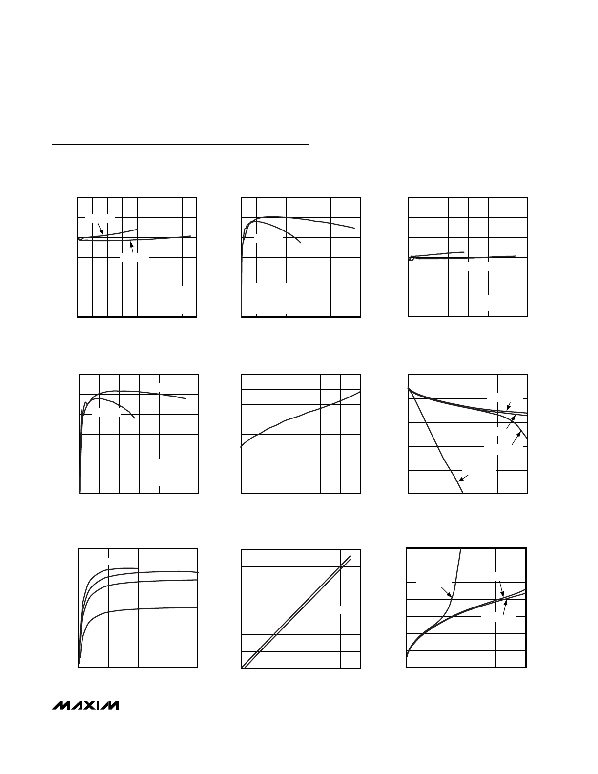
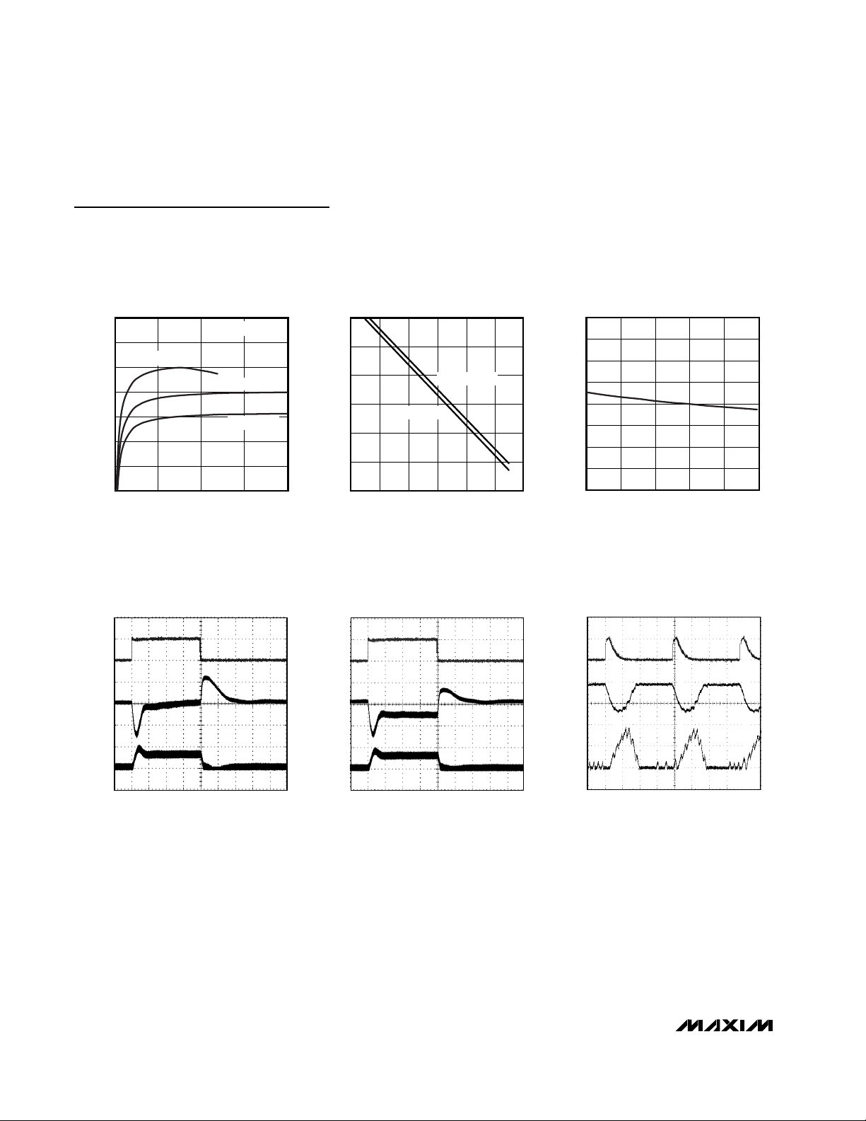
Typical Operating Characteristics
(Circuit of Figure 1, VIN= +3.3V, SHDN = IN, V
MAIN
= V
SUPP
= V
SUPN
= V
SUPB
= V
SUPL
= 8V, BUF- = BUFOUT,
BUF+ = FLTSET = TGND = PGND = GND, T
A
= +25°C.)
MAIN 8V OUTPUT VOLTAGE
vs. LOAD CURRENT
8.12
8.08
VIN = 3.3V
MAX1778 toc01
100
90
MAIN 8V OUTPUT EFFICIENCY
vs. LOAD CURRENT
VIN = 5V
MAX1778 toc02
12.24
12.16
MAIN 12V OUTPUT VOLTAGE
vs. LOAD CURRENT
MAX1778 toc03
8.04
(V)
8.00
OUT
V
7.96
7.92
7.88
0 200 400 600 800
VIN = 5V
I
OUT
(mA)
R
C
C
COMP
COMP
INTG
= 470pF
= 24kΩ
= 470pF
MAIN 12V OUTPUT EFFICIENCY
vs. LOAD CURRENT
100
V
5V
=
(mA)
IN
FIGURE 8
V
OUT
C
INTG
= 12V
= 470pF
MAX1778 toc04
90
V
3.3V
=
IN
80
70
EFFICIENCY (%)
60
50
40
0 200 300100 400 500 600
I
OUT
POSITIVE CHARGE-PUMP EFFICIENCY
vs. LOAD CURRENT
100
V
= 7V
90
80
70
60
EFFICIENCY (%)
50
40
30
SUPP
01051520
I
NEG
(mA)
V
= 7.5V
SUPP
V
V
V
SUPP
SUPP
POS
MAX1778 toc07
= 8V
= 10V
= 20V
80
VIN = 3.3V
70
EFFICIENCY (%)
60
V
= 8V
OUT
= 24kΩ
R
COMP
50
40
= 470pF
C
COMP
= 470pF
C
INTG
0 200 400 600 800
I
(mA)
OUT
STEP UP CONVERTERS
SWITCHING FREQUENCY vs. INPUT VOLTAGE
1.20
MAX1778
1.15
1.10
1.05
1.00
0.95
0.90
SWITCHING FREQUENCY (MHz)
0.85
0.80
2.5 3.53.0 4.0 4.5 5.0 5.5
VIN (V)
MAXIMUM POSITIVE CHARGE-PUMP
OUTPUT VOLTAGE vs. SUPPLY VOLTAGE
40
35
30
25
(V)
POS
V
20
15
10
5
2684 101214
I
= 1mA
POS
I
= 10mA
POS
V
(V)
SUPP
MAX1778 toc05
MAX1778 toc08
12.08
V
3.3V
=
(V)
12.00
OUT
V
11.92
11.84
11.76
IN
V
5V
=
IN
FIGURE 8
= 470pF
C
INTG
0 200 300100 400 500 600
I
(mA)
OUT
POSITIVE CHARGE-PUMP OUTPUT VOLTAGE
vs. LOAD CURRENT
20.2
= 10V
= 7.5V
MAX1778 toc06
V
V
SUPP
(mA)
V
= 7V
SUPP
V
SUPP
= 8V
SUPP
20.0
19.8
(V)
POS
V
19.6
19.4
19.2
01051520
I
POS
NEGATIVE CHARGE-PUMP OUTPUT VOLTAGE
vs. LOAD CURRENT
-4.90
-4.92
V
= 7V
V
-4.94
-4.96
(V)
NEG
V
-4.98
-5.00
-5.02
-5.04
0 10203040
SUPN
= 6V
SUPN
V
= 8V
SUPN
I
(mA)
NEG
MAX1778 toc09
Page 10
MAX1778/MAX1880–MAX1885
Quad-Output TFT LCD DC-DC
Converters with Buffer
10 ______________________________________________________________________________________
Typical Operating Characteristics (continued)
(Circuit of Figure 1, VIN= +3.3V, SHDN = IN, V
MAIN
= V
SUPP
= V
SUPN
= V
SUPB
= V
SUPL
= 8V, BUF- = BUFOUT,
BUF+ = FLTSET = TGND = PGND = GND, T
A
= +25°C.)
30
50
40
70
60
90
80
100
NEGATIVE CHARGE-PUMP EFFICIENCY
vs. LOAD CURRENT
MAX1778 toc10
I
NEG
(mA)
EFFICIENCY (%)
0 10203040
V
SUPN
= 7V
V
SUPN
= 8V
V
SUPN
= 6V
V
NEG
= -5V
-14
-10
-12
-6
-8
-4
-2
2684 101214
MAXIMUM NEGATIVE CHARGE-PUMP
OUTPUT VOLTAGE vs. SUPPLY VOLTAGE
MAX1778 toc11
V
SUPN
(V)
V
NEG
(V)
I
NEG
= 10mA
I
NEG
= 1mA
1.23
1.24
1.25
1.26
1.27
0 20406080100
REFERENCE VOLTAGE
vs. REFERENCE LOAD CURRENT
MAX1778 toc12
I
REF
(µA)
V
REF
(V)
STEP-UP CONVERTER LOAD-TRANSIENT
RESPONSE
MAX1778 toc13
200mA
0
8.1V
8.0V
7.9V
1A
0
40µs/div
A. I
MAIN
= 20mA to 200mA, 200mA/div
B. V
MAIN
= 8V, 100mV/div
C. INDUCTOR CURRENT, 1A/div
C
INTG
= 1000pF
C
B
A
STEP-UP CONVERTER LOAD-TRANSIENT
RESPONSE WITHOUT INTEGRATOR
MAX1778 toc14
200mA
0
8.1V
8.0V
7.9V
1A
0
40µs/div
A. I
MAIN
= 20mA to 200mA, 200mA/div
B. V
MAIN
= 8V, 100mV/div
C. INDUCTOR CURRENT, 1A/div
INTG = REF
C
B
A
STEP-UP CONVERTER LOAD-TRANSIENT
RESPONSE (1µs PULSES)
MAX1778 toc15
0.5A
0
8.0V
7.9V
1A
0.5A
0
4µs/div
A. I
MAIN
= 0 to 500mA, 500mA/div
B. V
MAIN
= 8V, 100mV/div
C. INDUCTOR CURRENT, 500mA/div
C
B
A
Page 11
MAX1778/MAX1880–MAX1885
Quad-Output TFT LCD DC-DC
Converters with Buffer
______________________________________________________________________________________ 11
Typical Operating Characteristics (continued)
(Circuit of Figure 1, VIN= +3.3V, SHDN = IN, V
MAIN
= V
SUPP
= V
SUPN
= V
SUPB
= V
SUPL
= 8V, BUF- = BUFOUT,
BUF+ = FLTSET = TGND = PGND = GND, T
A
= +25°C.)
RIPPLE VOLTAGE WAVEFORMS
8V
-5V
20V
= 8V, I
A. V
MAIN
MAIN
= -5V, I
= 20V, I
= 10mA, 20mV/div
NEG
POS
B. V
C. V
NEG
POS
POWER-UP SEQUENCE
2V
0
5V
0
20V
10V
0
-10V
= O TO 2V, 2V/div
A. V
SHDN
B. RDY, 5V/div
C. POSITIVE CHARGE PUMP = V
D. STEP-UP CONVERTER: V
E. NEGATIVE CHARGE PUMP: V
1µs/div
= 200mA, 10mV/div
= 5mA, 20mV/div
2ms/div
MAIN
POS
= 8V, R
NEG
MAX1778 toc16
MAX1778 toc19
= 20V, R
LOAD
= -5V, R
= 4kΩ, 10V/div
LOAD
= 40Ω, 10V/div
= 500Ω, 10V/div
LOAD
A
B
C
A
B
C
D
E
2V
0
8V
6V
4V
0.5A
0
A. V
SHDN
B. V
MAIN
C. INDUCTOR CURRENT, 500mA/div
R
LOAD
4V
2V
0
20V
10V
0
0
-5V
A. RDY, 2V/div
B. POSITIVE CHARGE PUMP, V
C. STEP-UP CONVERTER: V
D. NEGATIVE CHARGE PUMP, V
STEP-UP CONVERTER
SOFT-START (LIGHT LOAD)
1ms/div
= O TO 2V, 2V/div
= 8V, 2V/div
= 400
Ω
POWER-UP SEQUENCE
(CIRCUIT OF FIG.10)
1ms/div
POS(SYS)
MAIN(SYS)
NEG
MAX1778 toc17
MAX1778 toc20
= 20V, 10V/div
= 8V, 10V/div
= -5V, -5V/div
A
B
C
A
B
C
D
SOFT-START (HEAVY LOAD)
2V
0
8V
6V
4V
1.0A
0.5A
0
= O TO 2V, 2V/div
A. V
SHDN
= 8V, 2V/div
B. V
MAIN
C. INDUCTOR CURRENT, 500mA/div
= 20
R
LOAD
POWER-UP INTO SHORT-CIRCUIT
4V
2V
0
5V
0
10V
5V
0
A. RDY, 2V/div
B. GATE OF N-CH MOSFET, 5V/div
C. STEP-UP CONVERTER, V
V
MAIN(SYS)
STEP-UP CONVERTER
MAX1778 toc18
1ms/div
Ω
(CIRCUIT OF FIG. 10)
100µs/div
= GND
MAIN(START)
MAX1778 toc21
= 8V, 5V/div
A
B
C
A
B
C
Page 12
MAX1778/MAX1880–MAX1885
Quad-Output TFT LCD DC-DC
Converters with Buffer
12 ______________________________________________________________________________________
Typical Operating Characteristics (continued)
(Circuit of Figure 1, VIN= +3.3V, SHDN = IN, V
MAIN
= V
SUPP
= V
SUPN
= V
SUPB
= V
SUPL
= 8V, BUF- = BUFOUT,
BUF+ = FLTSET = TGND = PGND = GND, T
A
= +25°C.)
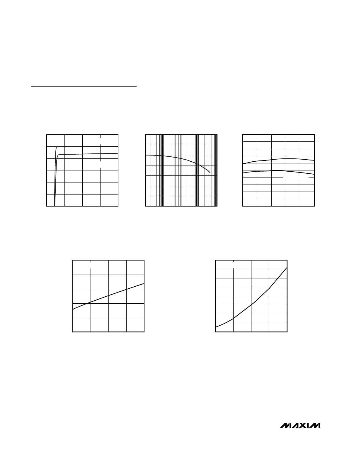
LDO OUTPUT VOLTAGE
vs. LDO INPUT VOLTAGE
(INTERNAL LINEAR REGULATOR)
5.05
I
= 0
(V)
LDOOUT
I
LDOOUT
MAX1778 toc22
= 40mA
5.00
4.95
(V)
4.90
LDOOUT
V
4.85
4.80
4.75
4861012
V
SUPL
5.04
5.02
5.00
(V)
4.98
LDOOUT
4.96
V
4.94
4.92
4.90
0.01 0.1 10 100
LDO OUTPUT VOLTAGE
vs. LDO OUTPUT CURRENT
(INTERNAL LINEAR REGULATOR)
1
I
(mA)
LDOOUT
DROPOUT VOLTAGE
vs. LDO LOAD CURRENT
(INTERNAL LINEAR REGULATOR)
200
V
= 5V
LDOOUT
160
(mV)
120
LDOOUT
- V
80
SUPL
V
40
0
02010 30 40
I
(mA)
LDOOUT
MAX1778 toc25
LDO OUTPUT VOLTAGE vs. TEMPERATURE
(INTERNAL LINEAR REGULATOR)
5.10
5.08
MAX1778 toc23
5.06
5.04
5.02
(V)
5.00
LDO
V
4.98
4.96
4.94
4.92
4.90
-40 10-15 35 60 85
TEMPERATURE (°C)
LDO SUPPLY CURRENT
vs. LDO OUTPUT CURRENT
(INTERNAL LINEAR REGULATOR)
4.0
V
= 5V
LDOOUT
3.5
3.0
(mA)
2.5
2.0
LDOOUT
- I
1.5
SUPL
I
1.0
0.5
0
0 10203040
I
(mA)
LDOOUT
I
LDOOUT
I
LDOOUT
MAX1778 toc24
= 0
= 40mA
MAX1778 toc26
Page 13

MAX1778/MAX1880–MAX1885
Quad-Output TFT LCD DC-DC
Converters with Buffer
______________________________________________________________________________________ 13
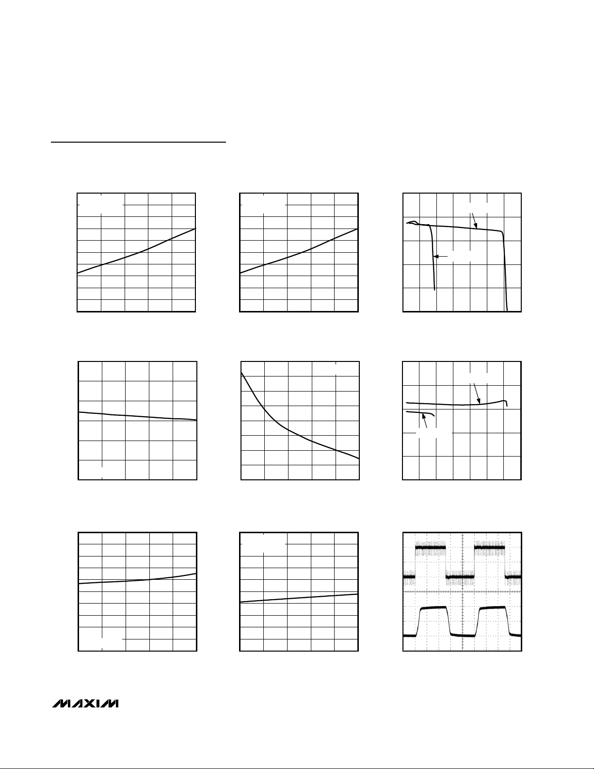
Typical Operating Characteristics (continued)
(Circuit of Figure 1, VIN= +3.3V, SHDN = IN, V
MAIN
= V
SUPP
= V
SUPN
= V
SUPB
= V
SUPL
= 8V, BUF- = BUFOUT,
BUF+ = FLTSET = TGND = PGND = GND, T
A
= +25°C.)
POWER-SUPPLY REJECTION RATIO
vs. FREQUENCY
100
80
60
PSRR (dB)
40
20
C
= 4.7µF
LDOOUT
= 40mA
I
LDOOUT
0
1100010010
FREQUENCY (kHz)
LOAD-TRANSIENT RESPONSE NEAR
DROPOUT (INTERNAL LINEAR REGULATOR)
MAX1778 toc30
MAX1778 toc27
100
10
ESR (Ω)
1
LDOOUT
C
0.1
0.01
040
REGION OF STABLE C
LDOOUT
vs. LOAD CURRENT
C
LDOOUT
STABLE REGION
10 20 30
I
(mA)
LDOOUT
INTERNAL LINEAR-REGULATOR
RIPPLE REJECTION
ESR
= 1µF
MAX1778 toc31
MAX1778 toc28
4OmA
5.00V
4.96V
LOAD-TRANSIENT RESPONSE
(INTERNAL LINEAR REGULATOR)
0
100µs/div
A. I
= 100µA TO 40mA, 40mA/div
LDO
= 5V, 20mV/div
B. V
LDO
= V
LDO
+ 500mV
V
SUPL
INTERNAL LINEAR-REGULATOR
STARTUP
MAX1778 toc29
A
B
MAX1778 toc32
4OmA
5.00V
4.94V
0
A. I
= 100µA TO 40mA, 40mA/div
LDO
= 5V, 20mV/div
B. V
LDO
= V
+ 100mV
V
IN
LDO
2V
A
B
C
0
4V
2V
0
4V
2V
A. V
S
HDN
B. V
LDOOUT
C. V
MAIN
400µs/div
= 0 TO 2V, 2V/div
= 5V, R
LDOOUT
= 8V, R
= 40Ω, 2V/div
MAIN
= 125Ω, 2V/div
100µs/div
5.0V
A
8.0V
B
1.0A
0.5A
0
10µs/div
A. V
= 5V, I
LDOOUT
= V
B. V
MAIN
SUPL
= 0 TO 750mA, 500mA/div
C. I
MAIN
= 40mA, 10mV/div
LDOOUT
= 8V, 200mV/div
A
B
C
Page 14

MAX1778/MAX1880–MAX1885
Quad-Output TFT LCD DC-DC
Converters with Buffer
14 ______________________________________________________________________________________
Typical Operating Characteristics (continued)
(Circuit of Figure 1, VIN= +3.3V, SHDN = IN, V
MAIN
= V
SUPP
= V
SUPN
= V
SUPB
= V
SUPL
= 8V, BUF- = BUFOUT,
BUF+ = FLTSET = TGND = PGND = GND, T
A
= +25°C.)
LINEAR-REGULATOR OUTPUT VOLTAGE
vs. INPUT VOLTAGE
(EXTERNAL LINEAR REGULATOR)
2.55
2.53
I
I
LDO
LDO
= 750mA
VIN (V)
= 0
2.51
(V)
LDO
V
2.49
2.47
FIGURE 7
2.45
2.5 3.53.0 4.0 4.5 5.0 5.5
MAX1778 toc33
EXTERNAL LINEAR-REGULATOR
RIPPLE REJECTION
2.5V
8.0V
7.8V
1A
0.5A
0
10µs/div
A. V
= 2.5V, I
= V
SUPL
= 200mA, 10mV/div
LDO
= 8V, 200mV/div
LDO
B. V
MAIN
= 0 TO 750mA, 500mA/div
C. I
MAIN
FIGURE 7
MAX1778 toc36
A
B
C
LINEAR-REGULATOR OUTPUT VOLTAGE
vs. LOAD CURRENT
(EXTERNAL LINEAR REGULATOR)
2.55
2.53
2.51
(V)
LDO
V
2.49
2.47
2.45
0.1 1 10 100 1000
I
(mA)
LDO
INPUT OFFSET VOLTAGE DEVIATION
vs. COMMON-MODE VOLTAGE
2.5
1.5
V
= 4.5V
SUPB
0.5
(mV)
OS
∆V
-0.5
-1.5
-2.5
02468101214
VCM (V)
V
= 13V
SUPB
FIGURE 7
MAX1778 toc34
MAX1778 toc37
EXTERNAL LINEAR-REGULATOR
250mA
50mA
2.55V
2.50V
2.45V
LOAD-TRANSIENT RESPONSE
100µs/div
A. I
= 50mA TO 250mA, 200mA/div
LDO
= 2.5V, 50mV/div
B. V
LDO
FIGURE 7
MAX1778 toc35
INPUT OFFSET VOLTAGE DEVIATION
vs. BUFFER SUPPLY VOLTAGE
1.0
0.6
0.2
(mV)
OS
∆V
-0.2
-0.6
-1.0
486101214
V
SUPB
(V)
VCM = V
SUPB
/ 2
A
B
MAX1778 toc38
Page 15
MAX1778/MAX1880–MAX1885
Quad-Output TFT LCD DC-DC
Converters with Buffer
______________________________________________________________________________________ 15
Typical Operating Characteristics (continued)
(Circuit of Figure 1, VIN= +3.3V, SHDN = IN, V
MAIN
= V
SUPP
= V
SUPN
= V
SUPB
= V
SUPL
= 8V, BUF- = BUFOUT,
BUF+ = FLTSET = TGND = PGND = GND, T
A
= +25°C.)
INPUT OFFSET VOLTAGE DEVIATION
vs. TEMPERATURE
1.0
V
= 13V
SUPB
= V
CM
/ 2
SUPB
TEMPERATURE (°C)
V
0.6
0.2
(mV)
OS
∆V
-0.2
-0.6
0
-40 10-15 35 60 85
BUFFER INPUT BIAS CURRENT
vs. BUFFER SUPPLY VOLTAGE
10
8
(nA)
BIAS
I
6
VCM = V
4
486 101214
SUPB
/ 2
V
(V)
SUPB
BUFFER SUPPLY CURRENT
vs. BUFFER SUPPLY VOLTAGE
0.50
0.46
0.42
(mA)
SUPB
I
0.38
0.34
VCM = V
0.30
486101214
SUPB
/ 2
V
(V)
SUPB
MAX1778 toc39
MAX1778 toc42
MAX1778 toc45
INPUT OFFSET VOLTAGE DEVIATION
1.0
V
V
0.6
0.2
(mV)
OS
∆V
-0.2
-0.6
0
-40 10-15 35 60 85
12
11
10
9
(nA)
8
BIAS
I
7
6
5
4
-40 -15 10 35 60 85
NO-LOAD BUFFER SUPPLY CURRENT
1.0
V
0.9
V
0.8
0.7
0.6
(mA)
0.5
SUPB
I
0.4
0.3
0.2
0.1
0
-40 10-15 35 60 85
vs. TEMPERATURE
= 13V
SUPB
= V
/ 2
CM
SUPB
TEMPERATURE (°C)
BUFFER INPUT BIAS CURRENT
vs. TEMPERATURE
VCM = V
TEMPERATURE (°C)
vs. TEMPERATURE
= 13V
SUPB
= V
/ 2
CM
SUPB
TEMPERATURE (°C)
SUPB
MAX1778 toc39
/ 2
MAX1778 toc43
MAX1778 toc46
(mA)
SUPB
I
BUFFER INPUT BIAS CURRENT
vs. COMMON-MODE VOLTAGE
10
V
= 13V
V
SUPB
VCM (V)
SUPB
= 4.5V
8
6
(nA)
BIAS
I
4
2
0
042 6 8 101214
BUFFER SUPPLY CURRENT
vs. COMMON-MODE VOLTAGE
0.50
V
= 13V
0.46
0.42
V
0.38
0.34
0.30
042 6 8 101214
SUPB
= 4.5V
SUPB
VCM (V)
VCOM BUFFER
SMALL-SIGNAL RESPONSE
4.05V
4.00V
3.95V
4.05V
4.00V
3.95V
4µs/div
A. V
= 3.95V TO 4.05V, 50mV/div
BUF+
B. BUFOUT = BUF-, 50mV/div
C
BUF
= 1µF, V
SUPB
= 8V
MAX1778 toc41
MAX1778 toc44
MAX1778 toc47
A
B
Page 16

MAX1778/MAX1880–MAX1885
Quad-Output TFT LCD DC-DC
Converters with Buffer
16 ______________________________________________________________________________________
Typical Operating Characteristics (continued)
(Circuit of Figure 1, VIN= +3.3V, SHDN = IN, V
MAIN
= V
SUPP
= V
SUPN
= V
SUPB
= V
SUPL
= 8V, BUF- = BUFOUT,
BUF+ = FLTSET = TGND = PGND = GND, T
A
= +25°C.)
MAX1778 toc51
C
B
A
8.1V
7.8V
2V
4V
2V
0
4V
0
100µs/div
VCOM BUFFER STARTUP
A. RDY, 2V/div
B. BUFOUT = BUF-, C
BUF
= 1µF, 2V/div
C. V
SUPB
= V
MAIN
= 8V, I
MAIN
= 20mA, 200mV/div
BUF+ = GND
MAX1778 toc51
C
B
A
8.1V
7.8V
2V
4V
2V
0
4V
0
100µs/div
VCOM BUFFER STARTUP
A. RDY, 2V/div
B. BUFOUT = BUF-, C
BUF
= 1µF, 2V/div
C. V
SUPB
= V
MAIN
= 8V, I
MAIN
= 20mA, 200mV/div
BUF+ = GND
LARGE-SIGNAL RESPONSE
4.50V
4.00V
3.50V
4.50V
4.00V
3.50V
A. V
= 3.50V TO 4.50V, 0.5V/div
BUF+
B. BUFOUT = BUF-, 0.5V/div
= 1µF, V
C
BUF
VCOM BUFFER
10µs/div
= 8V
SUPB
MAX1778 toc48
200mA
A
B
0
-200mA
4.2V
4.0V
3.8V
8.0V
A. I
BUFOUT
B. BUFOUT = BUF-, 200mV/div
C. V
V
SUPB
VCOM BUFFER
LOAD-TRANSIENT RESPONSE
4µs/div
= 200mA PULSES, 200mA/div
= 8V, 50mV/div
MAIN
= V
, BUF+ = GND, C
MAIN
BUF
= 1µF
MAX1778 toc49
VCOM BUFFER
LOAD-TRANSIENT RESPONSE
500mA
A
B
C
0
-500mA
4.5V
4.0V
3.5V
8.0V
A. I
BUFOUT
B. BUFOUT = BUF-, 0.5V/div
C. V
MAIN
= V
V
SUPB
4µs/div
= 400mA PULSES, 500mA/div
= 8V, 100mV/div
, BUF+ = GND, C
MAIN
BUF
MAX1778 toc50
A
B
C
= 1µF
Page 17

MAX1778/MAX1880–MAX1885
Quad-Output TFT LCD DC-DC
Converters with Buffer
______________________________________________________________________________________ 17
Pin Description
PIN
MAX1778
MAX1881
1111FB
2222INTG
3333IN
4444BUF+
5555BUF-
6666SUPB
7777BUFOUT VCOM Buffer (Operational Transconductance Amplifier) Output
8888GND
MAX1880
MAX1882
MAX1883
MAX1884
MAX1885 NAME FUNCTION
Main Step-Up Regulator Feedback Input. Regulates to 1.25V
nominal. Connect a resistive divider from the output (V
to analog ground (GND).
Main Step-Up Integrator Output. When using the integrator,
connect 1000pF to analog ground (GND). To disable the
integrator, connect INTG to REF.
Main Supply Voltage. The supply voltage powers the control
circuitry for all of the regulators and may range from 2.7V to 5.5V.
Bypass with a 0.1µF capacitor between IN and GND, as close to
the pins as possible.
VCOM Buffer (Operational Transconductance Amplifier) Positive
Feedback Input. Connect to GND to select the internal resistive
divider that sets the positive input to half the amplifier’s supply
voltage (V
VCOM Buffer (Operational Transconductance Amplifier) Negative
Feedback Input
VCOM Buffer (Operational Transconductance Amplifier) Supply
Voltage
Analog Ground. Connect to power ground (PGND) underneath the
IC.
BUF+
= V
SUPB
/2).
MAIN
) to FB
Internal Reference Bypass Terminal. Connect a 0.22µF ceramic
9999REF
10 10 −−FBP
11 11 −−FBN
12 12 10 10 SHDN
13 − 11 − SUPL
capacitor from REF to analog ground (GND). External load
capability up to 50µA.
Positive Charge-Pump Regulator Feedback Input. Regulates to
1.25V nominal. Connect a resistive divider from the positive
charge-pump output (V
Negative Charge-Pump Regulator Feedback Input. Regulates to
0V nominal. Connect a resistive divider from the negative chargepump output (V
Active-Low Shutdown Control Input. Pull SHDN low to force the
controller into shutdown. If unused, connect SHDN to IN for normal
operation. A rising edge on SHDN clears the fault latch.
Low-Dropout Linear Regulator Input Voltage. Can range from 4.5V
to 15V. Bypass with a 1µF capacitor to GND (see Capacitor
Selection and Regulator Stability). Connect both input pins
together externally.
) to FBP to analog ground (GND).
POS
) to FBN to the reference (REF).
NEG
Page 18
MAX1778/MAX1880–MAX1885
Quad-Output TFT LCD DC-DC
Converters with Buffer
18 ______________________________________________________________________________________
Pin Description (continued)
PIN
MAX1778
MAX1881
14 − 12 − LDOOUT
15 − 13 − FBL
16 16 14 14 FLTSET
17 17 −−SUPN
18 18 −−DRVN
19 19 −−SUPP
20 20 −−DRVP
21 21 17 17 PGND
MAX1880
MAX1882
MAX1883
MAX1884
MAX1885
22 22 18 18 LX
23 23 19 19 TGND Must be connected to ground.
24 24 20 20 RDY
− 13, 14, 15 15, 16
11, 12, 13,
15, 16
NAME FUNCTION
Linear Regulator Output. Sources up to 40mA. Bypass to GND with
a ceramic capacitor determined by:
Voltage Setting Input. Connect a resistive divider from the linear
regulator output (V
Fault Trip-Level Set Input. Connect to a resistive divider between
REF and GND to set the main step-up converter’s and positive
charge pump’s fault thresholds between 0.67 x V
. Connect to GND for the preset fault threshold (0.9 x V
V
REF
Negative Charge-Pump Driver Supply Voltage. Bypass to power
ground (PGND) with a 0.1µF capacitor.
Negative Charge-Pump Driver Output. Output high level is V
and low level is PGND.
Positive Charge-Pump Driver Supply Voltage. Bypass to power
ground (PGND) with a 0.1µF capacitor.
Positive Charge-Pump Driver Output. Output high level is V
and low level is PGND
Power Ground. Connect to analog ground (GND) underneath the
IC.
Main Step-Up Regulator Power MOSFET N-Channel Drain. Place
output diode and output capacitor as close to PGND as possible.
Active-Low, Open-Drain Output. Indicates all outputs are ready.
On-resistance is 125Ω (typ).
N.C. No Connection. Not internally connected.
I
CmsX
LDOOUT
.
≥
05
) to FBL to analog ground (GND).
LDOOUT
LDOOUT MAX
V
LDOOUT
()
and 0.85 x
REF
REF
SUPN
SUPP
).
Page 19

MAX1778/MAX1880–MAX1885
Quad-Output TFT LCD DC-DC
Converters with Buffer
______________________________________________________________________________________ 19
Detailed Description
The MAX1778/MAX1880–MAX1885 are highly efficient
multiple-output power supplies for thin-film transistor
(TFT) liquid crystal display (LCD) applications. The
devices contain one high-power step-up converter, two
low-power charge pumps, an operational transconductance amplifier (V
COM
buffer), and a low-dropout linear
regulator. The primary step-up converter uses an internal N-channel MOSFET to provide maximum efficiency
and to minimize the number of external components.
The output voltage of the main step-up converter
(V
MAIN
) can be set from VINto 13V with external resis-
tors.
The dual charge pumps (MAX1778/MAX1880/
MAX1881/MAX1882 only) independently regulate a
positive output (V
POS
) and a negative output (V
NEG
).
These low-power outputs use external diode and
capacitor stages (as many stages as required) to regulate output voltages from -40V to +40V. A unique
control scheme minimizes output ripple as well as
capacitor sizes for both charge pumps.
A resistor-programmable 40mA linear regulator
(MAX1778/MAX1881/MAX1883/MAX1884 only) can
provide preregulation or postregulation for any of the
supplies. For higher current applications, an external
transistor can be added.
Additionally, the V
COM
buffer provides a high current
output that is ideal for driving capacitive loads, such as
the backplane of a TFT LCD panel. The positive feedback input features dual mode operation, allowing this
input to be connected to an internal 50% resistivedivider between the buffer’s supply voltage and
ground, or externally adjusted for other voltages.
Also included in the MAX1778/MAX1880–MAX1885 is a
precision 1.25V reference that sources up to 50µA,
logic shutdown, soft-start, power-up sequencing,
adjustable fault detection, thermal shutdown, and an
active-low, open-drain ready output.
Figure 1. Typical Application Circuit
V
= 3.3V
IN
INPUT
V
4.7µF
LDOOUT
NEGATIVE
V
NEG
C
IN
TO LOGIC
LDO
= 5V
= -5V
C
4.7µF
1.0µF
LDO
C3
R
RDY
100kΩ
0.22µF
49.9kΩ
C
0.22µF
MAIN
(8V)
R8
200kΩ
49.9kΩ
REF
L1
6.8µH
274kΩ
49.9kΩ
C4
0.1µF
C4
0.1µF
R2
R2
750kΩ
R4
49.9kΩ
R3
BUFFER OUTPUT
V
C
BUF
1.0µF
BUFOUT
LX
FB
SUPB
SUPN
SUPP
DRVP
FBP
BUFOUT
BUF-
BUF+
GND
TGND
R7
150kΩ
C2
0.1µF
IN
SHDN
RDY
SUPL
LDOOUT
MAX1778
FBL
DRVN
FBN
REF
INTG
FLTSET
PGND
C1
R5
R6
C
OUT
(2) 4.7µF
C5
1.0µF
= V
MAIN
V
SUPB
MAIN
C7
1.0µF
/2
= 8V
POSITIVE
V
POS
= 20V
Page 20

MAX1778/MAX1880–MAX1885
Quad-Output TFT LCD DC-DC
Converters with Buffer
20 ______________________________________________________________________________________
Main Step-up Controller
During normal pulse-width modulation (PWM) operation, the MAX1778/MAX1880–MAX1885 main step-up
controllers switch at a constant frequency of 500kHz or
1MHz (see Selector Guide), allowing the use of lowprofile inductors and output capacitors. Depending on
the input-to-output voltage ratio, the controller regulates
the output voltage and controls the power transfer by
modulating the duty cycle (D) of each switching cycle:
On the rising edge of the internal clock, the controller
sets a flip-flop when the output voltage is too low, which
turns on the N-channel MOSFET (Figure 2). The inductor current ramps up linearly, storing energy in a magnetic field. Once the sum of the feedback voltage error
amplifier, slope-compensation, and current-feedback
signals trip the multi-input comparator, the MOSFET
turns off, the flip-flop resets, and the diode (D1) turns
on. This forces the current through the inductor to ramp
back down, transferring the energy stored in the magnetic field to the output capacitor and load. The MOSFET remains off for the rest of the clock cycle. Changes
in the feedback voltage-error signal shift the switch-current trip level, consequently modulating the MOSFET
duty cycle.
Under very light loads, an inherent switchover to pulseskipping takes place (Figure 3). When this occurs, the
controller skips most of the oscillator pulses in order to
reduce the switching frequency and gate charge losses. When pulse-skipping, the step-up controller initiates
a new switching cycle only when the output voltage
drops too low. The N-channel MOSFET turns on, allowing the inductor current to ramp up until the multi-input
comparator trips. Then, the MOSFET turns off and the
diode turns on, forcing the inductor current to ramp
down. When the inductor current reaches zero, the
diode turns off, so the inductor stops conducting current. This forces the threshold between pulse-skipping
and PWM operation to coincide with the boundary
between continuous and discontinuous inductor-current operation:
Figure 2. Main Step-Up Converter block Diagram
VV
MAIN IN
D
≈
V
MAIN
-
I
LOAD CROSSOVER
ILIM
OSC
(80% DUTY)
S
R
Q
LX
I
LIM
PGND
FB
MAX1778
MAX1880
MAX1881
MAX1882
MAX1883
MAX1884
MAX1885
PWM
COMPARATOR
COMPARATOR
1
2
(2.7V TO 5.5V)
V
(UP TO 13V)
V
V
MAIN
V
IN
MAIN
R1
R
COMP
(OPTIONAL)
≈
C
IN
C
OUT
()
L1
D1
IN
2
VV
MAIN IN
fL
OSC
-
C
R1
R2
COMP
(OPTIONAL)
REF
ERROR
AMPLIFIER
INTG
g
m
C
INTG
V
REF
1.25V
REF
GND
R2
C
REF
V
= 1 + V
MAIN
( )
V
= 1.25V
REF
Page 21

MAX1778/MAX1880–MAX1885
Quad-Output TFT LCD DC-DC
Converters with Buffer
______________________________________________________________________________________ 21
The switching waveforms will appear noisy and asynchronous when light loading causes pulse-skipping
operation; this is a normal operating condition that
improves light-load efficiency.
Dual Charge-Pump Regulator (MAX1778/
MAX1880/MAX1881/MAX1882 Only)
The MAX1778/MAX1880/MAX1881/MAX1882 controllers contain two independent low-power charge
pumps (Figure 4). One charge pump inverts the input
voltage and provides a regulated negative output voltage. The second charge pump doubles the input voltage and provides a regulated positive output voltage.
The controllers contain internal P-channel and N-channel MOSFETs to control the power transfer. The
internal MOSFETs switch at a constant frequency
(fCHP = fOSC/2).
Positive Charge Pump
During the first half-cycle, the N-channel MOSFET turns
on and charges flying capacitor C
X(POS)
(Figure 4).
This initial charge is controlled by the variable N-channel on-resistance. During the second half-cycle, the Nchannel MOSFET turns off and the P-channel MOSFET
turns on, level shifting C
X(POS)
by V
SUPP
volts. This
connects C
X(POS)
in parallel with the reservoir capaci-
tor C
OUT(POS)
. If the voltage across C
OUT(POS)
plus a
diode drop (V
POS
+ V
DIODE
) is smaller than the level-
shifted flying capacitor voltage (V
CX(POS)
+ V
SUPP
),
charge flows from C
X(POS)
to C
OUT(POS)
until the diode
(D3) turns off.
Figure 3. Discontinuous-to-Continuous Conduction Crossover
Point
Figure 4. Low-Power Charge Pump Block Diagram
I
PEAK
I
INDUCTOR CURRENT
t
ON
t
OFF
TIME
LOAD
V
SUPP
2.7V TO 13V
V
SUPD
V
POS
V
= 1 + V
POS
V
= 1.25V
REF
C
OUT(POS)
R3
( )
R4
D2
C
X(POS)
D3
R3
R4
REF
SUPP
DRVP
FBP
1.25V
V
REF
MAX1778
MAX1880
MAX1881
MAX1882
OSC
SUPN
D4
C
X(NEG)
DRVN
D5
R6
C
REF
0.22µF
R5
FBN
REF
PGNDGND
V
NEG
V
REF
C
OUT(NEG)
R5
= - V
( )
R6
= 1.25V
V
SUPN
2.7V TO 13V
V
NEG
REF
Page 22

MAX1778/MAX1880–MAX1885
Quad-Output TFT LCD DC-DC
Converters with Buffer
22 ______________________________________________________________________________________
Negative Charge Pump
During the first half-cycle, the P-channel MOSFET turns
on, and flying capacitor C
X(NEG)
charges to V
SUPN
minus a diode drop (Figure 4). During the second halfcycle, the P-channel MOSFET turns off, and the Nchannel MOSFET turns on, level shifting C
X(NEG)
. This
connects C
X(NEG)
in parallel with reservoir capacitor
C
OUT(NEG)
. If the voltage across C
OUT(NEG)
minus a
diode drop is greater than the voltage across C
X(NEG)
,
charge flows from C
OUT(NEG)
to C
X(NEG)
until the diode
(D5) turns off. The amount of charge transferred to the
output is controlled by the variable N-channel on-resistance.
Low-Dropout Linear Regulator (MAX1778/
MAX1881/MAX1883/MAX1884 Only)
The MAX1778/MAX1881/MAX1883/MAX1884 contain a
low-dropout linear regulator (Figure 5) that uses an
internal PNP pass transistor (QP) to supply loads up to
40mA. As illustrated in Figure 5, the 1.25V reference is
connected to the error amplifier, which compares this
reference with the feedback voltage and amplifies the
difference. If the feedback voltage is higher than the
reference voltage, the controller lowers the base current of QP, which reduces the amount of current to the
output. If the feedback voltage is too low, the device
increases the pass transistor base current, which
allows more current to pass to the output and increases
the output voltage. However, the linear regulator also
includes an output current limit to protect the internal
pass transistor against short circuits.
The low-dropout linear regulator monitors and controls
the pass transistor’s base current, limiting the output
current to 130mA (typ). In conjunction with the thermal
overload protection, this current limit protects the output, allowing it to be shorted to ground for an indefinite
period of time without damaging the part.
VCOM Buffer
The MAX1778/MAX1880–MAX1885 include a VCOM
buffer, which uses an operational transconductance
amplifier (OTA) to provide a current output that is ideal
for driving capacitive loads, such as the backplane of a
TFT LCD panel. The unity-gain bandwidth of this current-output buffer is:
GBW = gm/C
OUT
where gm is the amplifier’s transconductance. The
bandwidth is inversely proportional to the output
capacitor, so large capacitive loads improve stability;
however, lower bandwidth decreases the buffer’s transient response time. To improve the transient response
Figure 5. Low-Dropout Linear Regulator Block Diagram
MAX1778
MAX1881
MAX1883
MAX1884
ERROR
AMPLIFIER
THERMAL
SENSOR
CURRENT
LIMIT
V
REF
1.25V
SUPL
LDOOUT
FBL
GND
C
SUPL
Q
P
C
R7
R8
LDOOUT
V
LDOOUT
V
REF
= 1.25V
V
SUPL
4.5V TO 15V
V
LDOOUT
1.25V TO (V
R7
= (1 + )V
R8
SUPL
- 0.3V)
REF
Page 23
MAX1778/MAX1880–MAX1885
Quad-Output TFT LCD DC-DC
Converters with Buffer
______________________________________________________________________________________ 23
times, the amplifier’s transconductance increases as
the output current increases (see Typical Operating
Characteristics).
The VCOM buffer’s positive feedback input features
dual mode operation. The buffer’s output voltage can
be internally set by a 50% resistive divider connected
to the buffer’s supply voltage (SUPB), or the output voltage can be externally adjusted for other voltages.
Shutdown (SHDN)
A logic-low level on SHDN shuts down all of the converters and the reference. When shut down, the supply
current drops to 0.1µA to maximize battery life, and the
reference is pulled to ground. The output capacitance,
feedback resistors, and load current determine the rate
at which each output voltage will decay. A logic-level
high on SHDN power activates the MAX1778/
MAX1880–MAX1885 (see Power-Up Sequencing). Do
not leave SHDN floating. If unused, connect SHDN to
IN. A logic-level transition on SHDN clears the fault
latch.
Power-Up Sequencing
Upon power-up or exiting shutdown, the MAX1778/
MAX1880–MAX1885 start a power-up sequence. First,
the reference powers up. Then, the main DC-DC stepup converter powers up with soft-start enabled. The linear regulator powers up at the same time as the main
step-up converter; however, the power sequence and
ready output signal are not affected by the regulation of
the linear regulator. While the main step-up converter
powers up, the output of the PWM comparator remains
low (Figure 2), and the step-up converter charges the
output capacitors, limited only by the maximum duty
cycle and current-limit comparator. When the step-up
converter approaches its nominal regulation value and
the PWM comparator’s output changes states for the
first time, the negative charge pump turns on. When the
negative output voltage reaches approximately 90% of
its nominal value (V
FBN
< 110mV), the positive charge
pump starts up. Finally, when the positive output voltage reaches 90% of its nominal value (V
FBP
> 1.125V),
the active-low ready signal (RDY) goes low (see Power
Ready), and the VCOM buffer powers up. The
MAX1883/MAX1884/MAX1885 do not contain the
charge pumps, but the power-up sequence still contains the charge pumps’ startup logic, which appears
as a delay (2 ✕4096/fOSC) between the step-up converter reaching regulation and when the ready signal
and VCOM buffer are activated.
Soft-Start
For the main step-up regulator, soft-start allows a gradual increase of the current-limit level during startup to
reduce input surge currents. The MAX1778/MAX1880–
MAX1885 divide the soft-start period into four phases.
During the first phase, the controller limits the current
limit to only 0.38A (see Electrical Characteristics),
approximately a quarter of the maximum current limit
Figure 6. VCOM Buffer Block Diagram
MAX1778
MAX1880
MAX1881
MAX1882
MAX1883
MAX1884
MAX1885
gm
125mV
SUPB
BUFOUT
BUF-
R
BUF+
R
GND
R11
R12
V
SUPB
4.5V TO 13V
C
BUF
V
BUFOUT
V
BUFOUT
1.2V TO (V
=
(
R11 + R12
SUPB
R12
)V
- 1.2V)
SUPB
Page 24

MAX1778/MAX1880–MAX1885
Quad-Output TFT LCD DC-DC
Converters with Buffer
24 ______________________________________________________________________________________
(I
LX(MAX)
). If the output does not reach regulation within
1ms, soft-start enters phase II, and the current limit is
increased by another 25%. This process is repeated for
phase III. The maximum 1.5A (typ) current limit is
reached within 3072 clock cycles or when the output
reaches regulation, whichever occurs first (see the
startup waveforms in the Typical Operating
Characteristics).
For the charge pumps (MAX1778/MAX1880/
MAX1881/MAX1882 only), soft-start is achieved by controlling the rate of rise of the output voltage. Both
charge-pump output voltages are controlled to be in
regulation within 4096 clock cycles, irregardless of output capacitance and load, limited only by the charge
pump’s output impedance. Although the MAX1883/
MAX1884/MAX1885 controllers do not include the
charge pumps, the soft-start logic still contains the
4096 clock cycle startup periods for both charge
pumps.
Fault Trip Level (FLTSET)
The MAX1778/MAX1880–MAX1885 feature dual mode
operation to allow operation with either a preset fault
trip level or an adjustable trip level for the step-up converter and positive charge-pump outputs. Connect FLTSET to GND to select the preset 0.9 ✕V
REF
fault
threshold. The fault trip level may also be adjusted by
connecting a voltage divider from REF to FLTSET
(Figure 8). For greatest accuracy, the total load on the
reference (including current through the negative
charge-pump feedback resistors) should not exceed
50µA so that VREF is guaranteed to be in regulation
(see Electrical Characteristics Table). Therefore, select
R10 in the 100kΩ to 1MΩ range, and calculate R9 with
the following equation:
R9 = R10 [(V
REF
/ V
FLTSET
) - 1]
where V
REF
= 1.25V, and V
FLTSET
may range from 0.67
x V
REF
to 0.85 x V
REF
. FLTSET’s input bias current has
a maximum value of 50nA. For 1% error, the current
through R10 should be at least 100 times the FLTSET
input bias current (I
FLTSET
).
Fault Condition
Once RDY is low, if the output of the main regulator or
either low-power charge pump falls below its fault
detection threshold, or if the input drops below its
undervoltage threshold, then RDY goes high impedance and all outputs shut down; however, the reference
remains active. After removing the fault condition, toggle shutdown (below 0.8V) or cycle the input voltage
(below 0.2V) to clear the fault latch and reactivate the
device.
The reference fault threshold is 1.05V. For the step-up
converter and positive charge-pump, the fault trip level is
set by FLTSET (see Fault Trip Level). For the negative
charge pump, the fault threshold measured at the
charge-pump’s feedback input (FBN) is 140mV (typ).
Power Ready (RDY)
Power ready is an open-drain output. When the powerup sequence for the main step-up converter and lowpower charge pumps has properly completed, the 14V
MOSFET turns on and pulls RDY low with a 125Ω (typ)
on-resistance. If a fault is detected on any of these
three outputs, the internal open-drain MOSFET appears
as a high impedance. Connect a 100kΩ pullup resistor
between RDY and IN for a logic-level output.
Voltage Reference (REF)
The voltage at REF is nominally 1.25V. The reference
can source up to 50µA with good load regulation (see
Typical Operating Characteristics). Connect a 0.22µF
ceramic bypass capacitor between REF and GND.
Thermal-Overload Protection
Thermal-overload protection limits total power dissipation in the MAX1778/MAX1880–MAX1885. When the
junction temperature exceeds T
J
= +160°C, a thermal
sensor activates the fault protection, which shuts down
the controller, allowing the IC to cool. Once the device
cools down by 15°C, toggle shutdown (below 0.8V) or
cycle the input voltage (below 0.2V) to clear the fault
latch and reactivate the controller. Thermal-overload
protection protects the controller in the event of fault
conditions. For continuous operation, do not exceed
the absolute maximum junction-temperature rating of
T
J
= +150°C.
Operating Region and Power Dissipation
The MAX1778/MAX1880–MAX1885s’ maximum power
dissipation depends on the thermal resistance of the IC
package and circuit board, the temperature difference
between the die junction and ambient air, and the rate
of any airflow. The power dissipated in the device
depends on the operating conditions of each regulator
and the buffer.
The step-up controller dissipates power across the
internal N-channel MOSFET as the controller ramps up
the inductor current. In continuous conduction, the
power dissipated internally can be approximated by:
P
STEP UP
IV
MAIN MAIN
≈
−
V
×
IN
RD
()
DS ON
22
+
12
1
VD
fL
OSC
IN
Page 25

MAX1778/MAX1880–MAX1885
Quad-Output TFT LCD DC-DC
Converters with Buffer
______________________________________________________________________________________ 25
where I
MAIN
includes the primary load current and the
input supply currents for the charge pumps (see
Charge-Pump Input Power and Efficiency
Considerations), linear regulator, and VCOM buffer.
The linear regulator generates an output voltage by dissipating power across an internal pass transistor, so
the power dissipation is simply the load current times
the input-to-output voltage differential:
When driving an external transistor, the internal linear
regulator provides the base drive current. Depending
on the external transistor’s current gain (β) and the
maximum load current, the power dissipated by the
internal linear regulator may still be significant:
The charge pumps provide regulated output voltages
by dissipating power in the low-side N-channel MOSFET, so they could be modeled as linear regulators followed by unregulated charge pumps. Therefore, their
power dissipation is similar to a linear regulator:
where N is the number of charge-pump stages, V
DIODE
is the diodes’ forward voltage, and V
SUPD
is the posi-
tive charge-pump diode supply (Figure 4).
The VCOM buffer’s power dissipation depends on the
capacitive load (C
LOAD
) being driven, the peak-to-
peak voltage change (V
P-P
) across the load, and the
load’s switching rate:
To find the total power dissipated in the device, the
power dissipated by each regulator and the buffer must
be added together:
The maximum allowed power dissipation is 975mW (24pin TSSOP) / 879mW (20-pin TSSOP) or:
P
MAX
= (T
J(MAX
) - TA) / ( θJB+ θBA)
where T
J
- TAis the temperature difference between
the controller’s junction and the surrounding air, θJB(or
θJC) is the thermal resistance of the package to the
board, and θBAis the thermal resistance from the printed circuit board to the surrounding air.
Design Procedure
Main Step-Up Converter
Output Voltage Selection
Adjust the output voltage by connecting a voltagedivider from the output (VMAIN) to FB to GND (see
Typical Operating Circuit). Select R2 in the 10kΩ to
50kΩ range. Calculate R1 with the following equations:
R1 = R2 [(V
MAIN
/ V
REF
) - 1]
where V
REF
= 1.25V. V
MAIN
may range from VINto 13V.
Inductor Selection
Inductor selection depends upon the minimum required
inductance value, saturation rating, series resistance, and
size. These factors influence the converter’s efficiency,
maximum output load capability, transient response time,
and output voltage ripple. For most applications, values
between 4.7µH and 22µH work best with the controller’s
switching frequency (Tables 1 and 2).
The inductor value depends on the maximum output
load the application must support, input voltage, output
voltage, and switching frequency. With high inductor
values, the MAX1778/MAX1880–MAX1885 source higher output currents, have less output ripple, and enter
continuous conduction operation with lighter loads;
however, the circuit’s transient response time is slower.
On the other hand, low-value inductors respond faster
to transients, remain in discontinuous conduction operation, and typically offer smaller physical size for a
given series resistance and current rating. The equations provided here include a constant LIR, which is the
ratio of the peak-to-peak AC inductor current to the
average DC inductor current. For a good compromise
between the size of the inductor, power loss, and output voltage ripple, select an LIR of 0.3 to 0.5. The
inductance value is then given by:
P
PIV VNV
NEG NEG SUPN DIODE NEG
PIV VNV V
POS POS SUPP DIODE SUPD POS
PIVV
LDO INT LDO SUPL LDO()
LDO INT
()
=
=
PVCfV
BUF P P LOAD LOAD SUPB
PP P
TOTAL STEP UP LDO INT
( )= -
I
LDO
.
=+
=
()
[]
()
[]
=
VV V
[]
β
IVV
( )
LDOOUT SUPL LDOOUT
--
--
-
=+
PPP
+++
NEG POS BUF
-
SUPL LDO
2
2
()
-
-
+
07
()
L
MIN
=
2
V
IN MIN
() ()
V
MAIN
VV
MAIN IN MIN
I f LIR
MAIN MAX OSC
-
()
1
η
Page 26
MAX1778/MAX1880–MAX1885
Quad-Output TFT LCD DC-DC
Converters with Buffer
26 ______________________________________________________________________________________
where η is the efficiency, f
OSC
is the oscillator frequen-
cy (see Electrical Characteristics), and I
MAIN
includes
the primary load current and the input supply currents
for the charge pumps (see Charge-Pump Input Power
and Efficiency Considerations), linear regulator, and
VCOM buffer. Considering the typical application circuit, the maximum average DC load current
(I
MAIN(MAX)
) is 300mA with an 8V output. Based on the
above equations and assuming 85% efficiency, the
inductance value is then chosen to be 4.7µH.
The inductor’s saturation current rating should exceed
the peak inductor current throughout the normal operating range. The peak inductor current is then given by:
Under fault conditions, the inductor current may reach
up to 1.85A (I
LIM(MAX)
), see Electrical Characteristics).
However, the controller’s fast current-limit circuitry
allows the use of soft-saturation inductors while still protecting the IC.
The inductor’s DC resistance may significantly affect
efficiency due to the power loss in the inductor. The
power loss due to the inductor’s series resistance (P
LR
)
may be approximated by the following equation:
where R
L
is the inductor’s series resistance. For best per-
formance, select inductors with resistance less than the
internal N-channel MOSFET on-resistance (0.35Ω typ).
Use inductors with a ferrite core or equivalent. To minimize radiated noise in sensitive applications, use a
shielded inductor.
Output Capacitor
Output capacitor selection depends on circuit stability
and output voltage ripple. A 10µF ceramic capacitor
works well in most applications (Tables 1 and 2).
Additional feedback compensation is required (see
Feedback Compensation) to increase the margin for
stability by reducing the bandwidth further. In cases
where the output capacitance is sufficiently large, additional feedback compensation will not be necessary.
Output voltage ripple has two components: variations in
the charge stored in the output capacitor with each LX
pulse, and the voltage drop across the capacitor’s
equivalent series resistance (ESR) caused by the current into and out of the capacitor:
where I
PEAK
is the peak inductor current (see Inductor
Selection). For ceramic capacitors, the output voltage
ripple is typically dominated by V
RIPPLE(C)
. The voltage
rating and temperature characteristics of the output
capacitor must also be considered.
Feedback Compensation
For stability, add a pole-zero pair from FB to GND in the
form of a compensation resistor (R
COMP
) in series with
a compensation capacitor (C
COMP
) as shown in Figure
2. Select R
COMP
to be half the value of R2, the low-side
feedback resistor.
Integrator Capacitor
The MAX1778/MAX1880–MAX1885 contain an internal
current integrator that improves the DC load regulation
but increases the peak-to-peak transient voltage (see
the load-transient waveforms in the Typical Operating
Characteristics). For highly accurate DC load regulation, enable the current integrator by connecting a
470pF (ƒ
OSC
= 1MHz)/1000pF (ƒ
OSC
= 500kHz)
capacitor to INTG. To minimize the peak-to-peak transient voltage at the expense of DC regulation, disable
the integrator by connecting INTG to REF. When using
the MAX1883/MAX1884/MAX1885, connect a 100kΩ
resistor to GND when disabling the integrator.
Input Capacitor
The input capacitor (CIN) in step-up designs reduces
the current peaks drawn from the input supply and
reduces noise injection. The value of CINis largely
determined by the source impedance of the input supply. High source impedance requires high input capacitance, particularly as the input voltage falls. Since
step-up DC-DC converters act as “constant-power
”
loads to their input supply, input current rises as input
voltage falls. A good starting point is to use the same
capacitance value for CINas for C
OUT
.
VV V
V I R AND
V
IV
()
I
PEAK
MAIN MAX MAIN
=
V
()
IN MIN
+
1
LIR
21η
PR
LR L
IXV
≅
MAIN MAIN
V
IN
2
RIPPLE RIPPLE C RIPPLE ESR
RIPPLE ESR PEAK ESR COUT
RIPPLE C
=+
() ( )
≈
()
() ( )
,
≈
VVVI
MAIN IN
MAIN
−
MAIN
Cf
OUT OSC
Page 27

MAX1778/MAX1880–MAX1885
Quad-Output TFT LCD DC-DC
Converters with Buffer
______________________________________________________________________________________ 27
Rectifier Diode
Use a Schottky diode with an average current rating
equal to or greater than the peak inductor current, and
a voltage rating at least 1.5 times the main output voltage (V
MAIN
).
Charge Pumps (MAX1778/ MAX1880/
MAX1881/MAX1882 Only)
Selecting the Number of Charge-Pump Stages
The number of charge-pump stages required to regulate the output voltage depends on the supply voltage,
output voltage, load current, switching frequency, the
diode’s forward voltage drop, and ceramic capacitor
values.
For positive charge-pump outputs, the number of
required stages may be determined by:
where V
SUPD
is the positive charge-pump diode supply
(Figure 4), V
DIODE
is the diode’s forward voltage drop,
and RTXis the charge pump’s output impedance. The
charge pump’s output impedance may be approximated using the following equation:
where the charge pump’s switching frequency (f
CHP
) is
equal to 0.5 x f
OSC
, the P-channel MOSFET’s on-resis-
tance (R
PCH(ON)
) is 10Ω, and the N-channel MOSFET’s
on-resistance (R
NCH(ON
)) is 4Ω (see Electrical
Characteristics).
For negative charge pump outputs, the number of
required stages may be determined by:
where N
NEG
is rounded up to the nearest integer.
Table 1. MAX1778/MAX1880/MAX1883 Component Values (f
OSC
= 1MHz)
*R
COMP
and C
COMP
are connected between the step-up converter’s output (V
MAIN
) and FB.
RR R
( )
=++
2
TX PCH ON NCH ON
+
Cf
N
POS
VVRI
SUPP DIODE TX LOAD
VV
-
POS SUPD
.( )
-112
+
≥
N
NEG
VVRI
CIRCUIT #1 CIRCUIT #2 CIRCUIT #3 CIRCUIT #4 CIRCUIT #5
V
IN
V
MAIN
I
MAIN(MAX)
V
NEG
I
NEG
V
POS
I
POS
L2.2µH4.7µH4.7µH6.8µH6.8µH
I
PEAK
C
OUT
R1 309kΩ 309kΩ 309kΩ 429kΩ 429kΩ
R2 49.9kΩ 49.9kΩ 49.9kΩ 49.9kΩ 49.9kΩ
R
COMP
C
COMP
3.3V 3.3V 3.3V 5V 5V
9V 9V 9V 12V 12V
100mA 200mA 200mA 220mA 220mA
-5V -5V -5V -5V -5V
2mA 5mA 5mA 5mA 5mA
24V 24V 24V 24V 24V
2mA 5mA 5mA 5mA 5mA
>1A >1A >1A >1A >1A
4.7µF10µF20µF10µF20µF
None None 39kΩ* None 20kΩ*
None None 100pF* None 200pF*
() ()
1
OUT CHP
Cf
1
X CHP
SUPN DROP TX LOAD
V
NEG
.( )
-112
+
≥
Page 28

MAX1778/MAX1880–MAX1885
Quad-Output TFT LCD DC-DC
Converters with Buffer
28 ______________________________________________________________________________________
Charge-Pump Input Power and
Efficiency Considerations
The charge pumps in the MAX1778/MAX1880/
MAX1881/MAX1882 provide regulated output voltages
by controlling the voltage drop across the low-side Nchannel MOSFET, so they can be modeled as linear
regulators followed by an unregulated charge pump
when determining the input power requirements and
efficiency.
The charge pump only provides charge to the output
capacitor during half the period (50% duty cycle), so
the input current is a function of the number of stages
and the load current:
for the positive charge pump, and:
for the negative charge pump, where N is the number
of charge pump stages.
The efficiency characteristics of the MAX1778/
MAX1880/MAX1881/MAX1882 regulated charge
pumps are similar to a linear regulator. It is dominated
by quiescent current at low output currents and by the
Table 2. MAX1881/MAX1882/MAX1884/MAX1885 Component Values (f
OSC
= 500kHz)
Table 3. Component Suppliers
*R
COMP
and C
COMP
are connected between the step-up converter’s output (V
MAIN
) and FB.
V
IN
V
MAIN
I
MAIN(MAX)
V
NEG
I
NEG
V
POS
I
POS
L4.7µH10µH10µH10µH
I
PEAK
C
OUT
R1 309kΩ 309kΩ 309kΩ 309kΩ
R2 49.9kΩ 49.9kΩ 49.9kΩ 49.9kΩ
R
COMP
C
COMP
CIRCUIT #6 CIRCUIT #7 CIRCUIT #8 CIRCUIT #9
3.3V 3.3V 3.3V 3.3V
9V 9V 9V 9V
100mA 100mA 200mA 200mA
-5V -5V -5V -5V
2mA 2mA 5mA 5mA
24V 24V 24V 24V
2mA 2mA 5mA 5mA
>1A >1A >1A >1A
4.7µF10µF10µF20µF
None None None 20kΩ*
None None None 200pF*
SUPPLIER PHONE FAX
INDUCTORS
Coilcraft 847-639-6400 847-639-1469
Coiltronics 561-241-7876 561-241-9339
Sumida USA 847-956-0666 847-956-0702
Toko 847-297-0070 847-699-1194
CAPACITORS
AVX 803-946-0690 803-626-3123
Kemet 408-986-0424 408-986-1442
Sanyo 619-661-6835 619-661-1055
Taiyo Yuden 408-573-4150 408-573-4159
DIODES
Central
Semiconductor
International
Rectifier
Motorola 602-303-5454 602-994-6430
Nihon 847-843-7500 847-843-2798
Zetex 516-543-7100 516-864-7630
516-435-1110 516-435-1824
310-322-3331 310-322-3332
IIN
SUPP POS
IIN
SUPP POS
() =+1
() =+1
Page 29

MAX1778/MAX1880–MAX1885
Quad-Output TFT LCD DC-DC
Converters with Buffer
______________________________________________________________________________________ 29
input voltage at higher output currents (see Typical
Operating Characteristics). So the maximum efficiency
may be approximated by:
for the positive charge pump, and:
for the negative charge pump, where V
SUPD
is the pos-
itive charge pump’s diode supply (Figure 4).
Output Voltage Selection
Adjust the positive output voltage by connecting a voltage divider from the output (V
POS
) to FBP to GND (see
Typical Operating Circuit). Adjust the negative output
voltage by connecting a voltage-divider from the output
(V
NEG
) to FBN to REF. Select R4 and R6 in the 50kΩ to
100kΩ range. Higher resistor values improve efficiency
at low output current but increase output voltage error
due to the feedback input bias current. For the negative
charge pump, higher resistor values also reduce the
load on the reference, which should not exceed 50µA
for greatest accuracy (including current through the
FLTSET resistors) to guarantee that V
REF
remains in
regulation (see Electrical Characteristics Table).
Calculate the remaining resistors with the following
equations:
R3 = R4 [(V
POS
/ V
REF
) - 1]
R5 = R6 |V
NEG
/ V
R
EF
|
where V
REF
= 1.25V. V
POS
may range from V
SUPP
to
40V, and V
NEG
may range from 0V to -40V.
Flying Capacitor
Increasing the flying capacitor (CX) value increases the
output current capability. Above a certain point,
increasing the capacitance has a negligible effect
because the output current capability becomes dominated by the internal switch resistance and the diode
impedance. The flying capacitor’s voltage rating must
exceed the following:
for the positive charge pump, and:
for the negative charge pump, where N is the stage
number in which the flying capacitor appears, and
V
SUPD
is the positive charge pump’s diode supply
(Figure 4). For example, the two-stage positive charge
pump in the typical application circuit (Figure 1) where
V
SUPP
= V
SUPD
= 8V contains two flying capacitors.
The flying capacitor in the first stage (C4) requires a
voltage rating over 12V. The flying capacitor in the second stage (C6) requires a voltage rating over 24V.
Charge-Pump Output Capacitor
Increasing the output capacitance or decreasing the
ESR reduces the output ripple voltage and the peak-topeak transient voltage. With ceramic capacitors, the
output voltage ripple is dominated by the capacitance
value. Use the following equation to approximate the
required capacitor value:
where f
CHP
is typically f
OSC
/2 (see Electrical
Characteristics).
Charge-Pump Input Capacitor
Use a bypass capacitor with a value equal to or greater
than the flying capacitor. Place the capacitor as close
to the IC as possible. Connect directly to power ground
(PGND).
Charge-Pump Rectifier Diodes
Use Schottky diodes with a current rating equal to or
greater than two times the average charge-pump input
current, and a voltage rating at least 1.5 times V
SUPP
for the positive charge pump and V
SUPN
for the nega-
tive charge pump.
Low-Dropout Linear Regulator (MAX1778/
MAX1881/MAX1883/MAX1884 Only)
Output Voltage Selection
Adjust the linear-regulator output voltage by connecting
a voltage-divider from LDOOUT to FBL to GND (Figure
5). Select R8 in the 5kΩ to 50kΩ range. Calculate R7
with the following equation:
R7 = R8 [(V
LDOOUT
/ V
FBL
) - 1]
where V
FBL
= 1.25V, and V
LDOOUT
may range from
1.25V to (V
SUPL
- 300mV). FBL’s input bias current is
η
POS
V
POS
≅+
VVN
SUPD SUPP
V
≅
VN
NEG
SUPN
η
NEG
VVVN
CXN POS SUPD SUPP()
. ( )>+
15 1-
[]
VVN
CXN NEG SUPN()
.( )> 15
C
≥
OUT
I
LOAD
fV
CHP RIPPLE
Page 30

MAX1778/MAX1880–MAX1885
Quad-Output TFT LCD DC-DC
Converters with Buffer
30 ______________________________________________________________________________________
0.8µA (max). For less than 0.5% error due to FBL input
bias current (I
F
BL
), R8 must be less than 8kΩ.
Capacitor Selection and Regulator Stability
Capacitors are required at the input and output of the
MAX1778/MAX1881/MAX1883/MAX1884 for stable
operation over the full temperature range and with load
currents up to 40mA. Connect a 1µF input bypass
capacitor (C
SUPL
) between SUPL and ground to lower
the source impedance of the input supply. Connect a
ceramic capacitor between LDOOUT and ground,
using the following equation to determine the lowest
value required for stable operation:
For example, with a 5V linear regulator output voltage
and a maximum 40mA load, use at least 4µF of output
capacitance. Applications that experience high-current
load pulses may require more output capacitance.
The ESR of the linear regulator’s output capacitor
(C
LDOOUT
) affects stability and output noise. Use out-
put capacitors with an ESR of 0.1Ω or less to ensure
stability and optimum transient response. Surfacemount ceramic capacitors are good for this purpose.
Place C
SUPL
and C
LDOOUT
as close to the linear regulator as possible to minimize the impact of PC board
trace inductance.
External Pass Transistor
For applications where the linear regulator currents
exceed 40mA or where the power dissipation in the IC
needs to be reduced, an external NPN transistor can
be used. In this case, the internal LDO only provides
the necessary base drive while the external NPN transistor supports the load, so most of the power dissipation occurs across the external transistor’s collector
and emitter.
Selection of the external NPN transistor is based on
three factors: the package’s power dissipation, the current gain (β), and the collector-to-emitter saturation voltage (V
CE(SAT)
). First, the maximum power dissipation
should not exceed the transistor’s package rating:
Once the appropriate package type is selected, consider the NPN transistor’s current gain. Since the internal LDO cannot source more than 40mA (min), the
transistor’s current gain must be high enough at the
lowest collector-to-emitter voltage to support the maximum output load:
For stable operation, place a capacitor (C
LDOOUT
) and
a minimum load resistor (R5) at the output of the internal linear regulator (the base of the external transistor)
to set the dominant pole:
Since the LDO cannot sink current, a minimum pulldown resistor (R5) is required at the base of the NPN
transistor to sink leakage currents and improve the
high-to-low load-transient response. Under no-load
conditions, leakage currents from the internal pass
transistor supply the output capacitor (C
LDOOUT
), even
when the transistor is off. As the leakage currents
increase over temperature, charge may build up on
C
LDOOUT
, making the linear regulator’s output rise
above its set point. Therefore, R5 must sink at least
100µA to guarantee proper regulation. Additionally, the
minimum load current provided by R5 improves the
high-to-low load transients by lowering the impedance
seen by C
LDOOUT
after the transient occurs. Therefore,
if large load transients are expected, select R5 so that
the minimum load current is 10% of the transistor’s
maximum base current:
Alternatively, output capacitance placed on the external
linear regulator’s output (the emitter) adds a second pole
that could destabilize the regulator. A capacitive-divider
from the transistor’s base to the feedback input (C2 and
C3, Figure 7) circumvents this second pole by adding a
pole-zero pair. Furthermore, to minimize excessive overshoot, the capacitive-divider’s ratio must be the same as
the resistive-divider’s ratio. Once the output capacitor is
selected, using the following equations to determine the
required capacitive-divider values:
N
CmsX
LDOOUT
.
≥
05
I
LDOOUT MAX
V
LDOOUT
()
R
PV V xI
( )
=−
COLLECTOR LDO LOAD MAX
()
ImA
β
MIN
Cms
LDOOUT
VV
x
LOAD MAX
≥
05
.
≥
+
07
.
LDO
R
5 β
-40
()
40
mA
1
V
LDO
I
LOAD MAX
+
()
MIN
5
=
CC
23
C
CCRRRVV
23434
VVIVV
LDO
LDOOUT MIN
+≥ +
2
+
07
.
+
.
() ( )
CR
LDO
100
=
+
( .)
LDO MI
01
=
4
1
R
=
3
LDO
+
I
LOAD MAX
REF
07
β
Page 31

MAX1778/MAX1880–MAX1885
Quad-Output TFT LCD DC-DC
Converters with Buffer
______________________________________________________________________________________ 31
Input-Output (Dropout) Voltage and Startup
A linear regulator’s minimum input-to-output voltage differential (dropout voltage) determines the lowest useable supply voltage. Because the MAX1778/
MAX1881/MAX1883/MAX1884 use an internal PNP
transistor (or external NPN transistor), their dropout
voltage is a function of the transistor’s collector-to-emitter saturation voltage (see Typical Operating
Characteristics). The linear regulator’s quiescent current increases when in dropout.
The internal linear regulator will try to start up once its
supply voltage (V
SUPL
) exceeds 4V. When the linear
regulator powers up, the linear regulator may be in
dropout if the linear regulator’s output set voltage is
higher than its input supply voltage. Therefore, during
this brief period, the linear regulator draws additional
supply current until the input supply voltage exceeds
the output set voltage plus the pass transistor’s saturation voltage (V
LDO(SET
) + V
CE(SAT)
).
VCOM Buffer (Operational
Transconductance Amplifier)
Buffer Output Voltage and Capacitor Selection
The positive input (BUF+) features dual mode operation. Connect BUF+ to GND for the preset VSUPB/2
output voltage, set by an internal 50% resistive-divider.
Adjust the amplifier’s output voltage by connecting a
voltage-divider from SUPB to BUF+ to GND (Figure 6).
Select R12 in the 10kΩ to 100kΩ range. Calculate R11
with the following equation:
where V
SUPB
may range from 4.5V to 13V, and V
BUF+
may range from 1.2V to (V
SUPB
- 1.2V). Connect a mini-
mum 1µF ceramic capacitor from BUFOUT to ground.
PC Board Layout and Grounding
Careful PC board layout is extremely important for
proper operation. Follow the following guidelines for
good PC board layout:
1) Place the main step-up converter output diode and
output capacitor less than 0.2in (5mm) from the LX
and PGND pins with wide traces and no vias.
2) Separate analog ground and power ground. The
ground connections for the step-up converter’s and
charge pump’s input and output capacitors should
be connected to the power ground plane. The linear regulator’s and VCOM buffer’s input and output
capacitors should be connected to a separate
power-ground path, star-connected to the PGND
pin to minimize voltage drops. When using multilayer boards, the top layer should contain the boost
Figure 7. External Linear Regulator
RR
11 12 1 =
V
SUPB
V
BUF
-
+
INPUT
= 3.3V
V
IN
C
4.7µF
IN
0.22µF
C
0.22µF
C1
REF
IN
SHDN
INTG
REF
PGND
L1
6.8µH
MAX1778
MAX1883
(MAX1881)*
(MAX1884)*
SUPL
LDOOUT
FBL
GND
MAIN
= 8V
V
OUT
Q1
C
LDOIN
1µF
R3
49.9kΩ
R4
49.9kΩ
MAIN
C
1µF
LDO
LDO
V
LDO
= 2.5V
C
LX
FB
274kΩ
49.9kΩ
R5
1.5kΩ
R1
R2
C
LDOOUT
4.7µF
C2
0.01µF
C3
0.01µF
(2) 4.7µF
Page 32

MAX1778/MAX1880–MAX1885
Quad-Output TFT LCD DC-DC
Converters with Buffer
32 ______________________________________________________________________________________
regulator and charge-pump power ground plane,
and the inner layer should contain the analog
ground plane and power-ground plane/path for the
V
COM
buffer and LDO. Connect all three ground
planes together at one place near the PGND pin.
3) Locate all feedback resistive-dividers as close to
their respective feedback pins as possible. The
voltage-divider’s center trace should be kept short.
Avoid running any feedback trace near the LX
switching node or the charge-pump drivers. The
resistive-dividers’ ground connections should be to
analog ground (GND).
4) When using multilayer boards, separate the top signal layer and bottom signal layer with a ground
plane between to eliminate capacitive coupling
between fast-charging nodes on the top layer and
high-impedance nodes on the bottom layer. The
fast-charging nodes, such as the LX and chargepump driver nodes, should not have any other
traces or ground planes near by.
5) Keep the charge-pump circuitry as close to the IC
as possible, using wide traces and avoiding vias
when possible. Place 0.1µF ceramic bypass
capacitors near the charge-pump input pins (SUPP
and SUPN) to the PGND pin.
6) To maximize output power and efficiency and minimize output ripple voltage, use extra wide, power
ground traces, and solder the IC’s power ground
pin directly to it.
Refer to the MAX1778/MAX1880-MAX1885 evaluation
kit for an example of proper board layout.
Figure 8. 5V Input Monitor Application
10µH
IN
SHDN
RDY
SUPL
V
IN
INPUT
= 5V
C
(2) 4.7µF
IN
TO LOGIC
R
RDY
100kΩ
C1
0.22µF
16.4kΩ
NEGATIVE
= -8V
V
NEG
Q1
R7
1.0µF
C
LDOOUT
4.7µF
C6
0.01µF
C3
C
REF
0.22µF
1.5kΩ
R5
316kΩ
49.9kΩ
LDO
= 3.3V
V
LDO
C6
1µF
R8
10kΩ
C7
0.01µF
R8
R6
C2
0.1µF
LDOOUT
MAX1778
FBL
DRVN
FBN
REF
INTG
PGND
L1
LX
FB
SUPB
SUPN
SUPP
DRVP
FBP
BUFOUT
BUF-
FLTSET
BUF+
GND
TGND
C4
0.1µF
86.6kΩ
10kΩ
R4
49.9kΩ
R1
R2
C
BUF
1.0µF
R10
100kΩ
R
4.7kΩ
R3
750kΩ
COMP
C
COMP
470pF
30kΩ
BUFFER OUTPUT
V
BUFOUT
R9
= V
SUPB
C5
1.0µF
C
OUT
(2) 10µF
/2
REF
MAIN
V
MAIN
POSITIVE
= 20V
V
POS
= 12V
Page 33

MAX1778/MAX1880–MAX1885
Quad-Output TFT LCD DC-DC
Converters with Buffer
______________________________________________________________________________________ 33
Applications Information
Low-Profile Components
Notebook applications generally require low-profile
components, potentially limiting the circuit’s performance. For example, low-profile inductors typically
have lower saturation ratings and more series resistance, limiting output current and efficiency. Low-profile
capacitors have lower voltage ratings for a given
capacitance value, so 3.3µF low-profile capacitors with
voltage ratings greater than 10V were not available at
the time of publication.
Desktop Monitors
Monitor applications do not have the same component
height restrictions associated with laptops, allowing
more flexibility in component selection (Figure 8).
Larger output capacitors with higher voltage ratings
allow configurations with output voltages above 10V.
Additionally, physically larger inductors with less series
resistance and higher saturation ratings provide more
output current and higher efficiency.
Input Voltage Above and
Below the Output Voltage
Combining the step-up converter and linear regulator
as shown in Figure 9 provides output voltage regulation
above and below the input voltage. Supplied by the
step-up converter, the linear regulator output provides
a constant output voltage (V
LDO
). When the input voltage exceeds the main step-up converter’s nominal output voltage, the controller stops switching but the linear
regulator maintains the output voltage. When the input
voltage drops below the output voltage, the step-up
Figure 9. Input Voltage Above and Below the Output Voltage
POWER INPUT
V
= 10V TO 15V
BATT
= 3.3V TO 5V
V
IN
TO LOGIC
BUFFER OUTPUT
V
= V
BUFOUT
V
/2
SUPB
NEGATIVE
= -12V
NEG
INPUT
1.0µF
0.22µF
C3
4.7µF
0.1µF
C
REF
C
IN
C1
R
RDY
100kΩ
C
BUF
1.0µF
475kΩ
100kΩ
C
INTG
470pF
R5
R10
49.9kΩ
30kΩ
R6
R9
C2
0.1µF
L1
6.8µH
IN
SHDN
RDY
BUFOUT
BUF-
MAX1778
DRVN
FBN
REF
FLTSET
INTG
PGND
C
OUT
C7
0.1µF
(3) 3.3µF
C
LDOOUT
3.3µF
6.8kΩ
R9
C5
1.0µF
Q1
POSITIVE
V
= 24V
POS
C
(2) 3.3µF
SUPL
LDOOUT
SUPB
SUPN
SUPP
FBL
DRVP
FBP
BUF+
GND
TGND
R1
511kΩ
LX
FB
0.1µF
C4
470kΩ
49.9kΩ
C6
0.1µF
R7
R4
49.9kΩ
R2
R8
49.9kΩ
R3
909kΩ
LDO
LDO
V
LDO
= 13V
Page 34

MAX1778/MAX1880–MAX1885
Quad-Output TFT LCD DC-DC
Converters with Buffer
34 ______________________________________________________________________________________
converter steps up the input voltage so that the linear
regulator will not drop out. Therefore, to guarantee that
the external pass transistor does not saturate, the stepup converter’s output voltage must be set above the linear regulator’s output voltage plus the transistor’s
saturation rating (V
MAIN
≥ V
LDO
+ V
SAT
).
Power-Up Sequencing and Fault Protection
The MAX1778/MAX1880–MAX1885’s fault protection
cannot be activated until the power-up sequence is
successfully completed and the power ready output
goes low. Therefore, faults on the main output or positive charge-pump output could damage the controller
or external components. Additional fault protection may
be added as shown in Figure 10. The external MOSFET
and PNP transistor isolate the positive outputs during
startup. When the controller finishes the power-up
sequence, the power-ready output goes low, turning on
the PNP transistor. Any fault on the positive chargepump output will pull down the charge pump’s output
voltage and trigger the fault protection; otherwise, the
MOSFET’s gate slow charges. Once the MOSFET turns
on, any faults on the main step-up converter’s output
will pull down the main output voltage and trigger the
fault protection.
VCOM Buffer Startup
The VCOM buffer does not include soft-start. Therefore,
once the VCOM buffer turns on, it draws high surge
currents while charging the output capacitance. In
some applications, the buffer’s high startup surge
current could potentially trip the fault detection circuit,
forcing the controller to shut down. In these cases,
adding a soft-start resistive divider between SUPB and
BUFOUT reduces the startup surge current and voltage
drops associated with this load (Figure 11), as shown in
Figure 10. Power-Up Sequencing and Fault Protection;
V
IN
INPUT
= 3.3V
C
4.7µF
C
REF
0.22µF
L1
6.8µH
IN
IN
C1
0.22µF
30kΩ
R10
100kΩ
SHDN
MAX1778
INTG
REF
R9
FLTSET
PGND
LX
FB
SUPP
DRVP
FBP
RDY
TGND
GND
274kΩ
49.9kΩ
C4
0.1µF
C6
0.1µF
R4
49.9kΩ
R1
R2
R3
750kΩ
STARTUP
POSITIVE
V
POS(START)
R
RDY
5.1kΩ
STARTUP MAIN
V
MAIN(START)
C10
0.1µF
C5
1.0µF
= 20V
C
OUT
(2) 3.3µF
= 8V
C7
1.0µF
Q3
Q2
100kΩ
SYSTEM MAIN
V
MAIN(SYS)
R7
10kΩ
SYSTEM
POSITIVE
V
POS(SYS)
R8
= 8V
C8
3.3µF
= 20V
INPUT
V
IN
= 3.3V
Page 35

the Typical Operating Characteristics. Set the resistive
divider to precharge BUFOUT, matching the buffer’s
output set voltage:
These resistor values are selected to charge the output
capacitor close to the output set voltage before the
buffer starts up:
MAX1778/MAX1880–MAX1885
Quad-Output TFT LCD DC-DC
Converters with Buffer
______________________________________________________________________________________ 35
Selector Guide
Figure 11. VCOM Buffer Soft-Start;
L1
IN
SHDN
INTG
REF
PGND
6.8µH
MAX1778
SUPB
BUF-
BUFOUT
BUF+
GND
INPUT
= 3.3V
V
IN
C
4.7µF
IN
0.22µF
C
0.22µF
C1
REF
RR
34 1 =
V
V
SUPB
BUFOUT
−
CRR
BUFOUT
(||) 34
≈
5000
f
OSC
MAIN
= 8V
V
OUT
[(
(Hz)
MAIN
BUFFER OUTPUT
V
BUFOUT
V
SUPB
) -1
V
BUFOUT
= V
/2
SUPB
]
DUAL
CHARGE
PUMPS
LINEAR
REGULATOR
C
LX
FB
R1
274kΩ
R2
49.9kΩ
R3
10kΩ
R4
10kΩ
PART
MAX1778 1M Yes Yes
MAX1880 1M Yes No
MAX1881 500k Yes Yes
MAX1882 500k Yes No
MAX1883 1M No Yes
MAX1884 500k No Yes
MAX1885 500k No No
(2) 4.7µF
C
SUPB
1.0µF
C
BUF
1.0µF
R3 = R4
STEP-UP
SWITCHING
FREQUENCY
Page 36

MAX1778/MAX1880–MAX1885
Quad-Output TFT LCD DC-DC
Converters with Buffer
36 ______________________________________________________________________________________
Typical Operating Circuit
INPUT
MAIN
LX
FB
SUPB
SUPN
SUPP
DRVP
FBP
BUFOUT
BUF-
BUF+
FLTSET
GND
TGND
TO LOGIC
LDO OUTPUT
NEGATIVE
IN
SHDN
RDY
SUPL
LDOOUT
FBL
DRVN
FBN
REF
INTG
PGND
MAX1778
POSITIVE
BUFFER OUTPUT
Page 37

MAX1778/MAX1880–MAX1885
Quad-Output TFT LCD DC-DC
Converters with Buffer
______________________________________________________________________________________ 37
Pin Configurations
TOP VIEW
INTG
BUF-
SUPB
BUFOUT
REF
FBP
FBN
SHDN
24
23
22
21
20
19
18
17
16
15
14
13
RDY
TGND
LX
PGNDBUF+
DRVP
SUPP
DRVN
SUPNGND
FLTSET
FBL
LDOOUT
SUPL
INTG
BUF-
SUPB
BUFOUT
REF
FBP
FBN
SHDN
1
FB
2
3
IN
4
MAX1880
5
MAX1882
6
7
8
9
10
11
12
1
FB
2
3
IN
4
MAX1778
5
MAX1881
6
7
8
9
10
11
12
24
RDY
23
TGND
22
LX
21
PGNDBUF+
20
DRVP
19
SUPP
18
DRVN
17
SUPNGND
16
FLTSET
15
N.C.
14
N.C.
13
N.C.
TOP VIEW
INTG
BUF-
SUPB
BUFOUT
REF
SHDN
FB
IN
1
2
3
4
5
6
7
8
9
10
24 TSSOP
MAX1883
MAX1884
20 TSSOP
20
19
18
17
16
15
14
13
12
11
RDY
TGND
LX
PGNDBUF+
N.C.
N.C.
FLTSET
FBLGND
LDOOUT
SUPL
INTG
BUF-
SUPB
BUFOUT
REF
SHDN
FB
IN
1
2
3
4
5
6
7
8
9
10
24 TSSOP
MAX1885
20 TSSOP
20
RDY
19
TGND
18
LX
17
PGNDBUF+
16
N.C.
15
N.C.
14
FLTSET
13
N.C.GND
12
N.C.
11
N.C.
Page 38

MAX1778/MAX1880–MAX1885
Quad-Output TFT LCD DC-DC
Converters with Buffer
Maxim cannot assume responsibility for use of any circuitry other than circuitry entirely embodied in a Maxim product. No circuit patent licenses are
implied. Maxim reserves the right to change the circuitry and specifications without notice at any time.
38 ____________________Maxim Integrated Products, 120 San Gabriel Drive, Sunnyvale, CA 94086 408-737-7600
© 2001 Maxim Integrated Products Printed USA is a registered trademark of Maxim Integrated Products.
Package Information
Chip Information
TRANSISTOR COUNT: 3739
TSSOP,NO PADS.EPS
 Loading...