

Page 1
General Description
The low-cost MAX1873R/S/T provides all functions
needed to simply and efficiently charge 2-, 3-, or 4series lithium-ion cells at up to 4A or more. It provides a
regulated charging current and voltage with less than
±0.75% total voltage error at the battery terminals. An
external P-channel MOSFET operates in a step-down
DC-DC configuration to efficiently charge batteries in
low-cost designs.
The MAX1873R/S/T regulates the battery voltage and
charging current using two control loops that work
together to transition smoothly between voltage and
current regulation. An additional control loop limits current drawn from the input source so that AC adapter
size and cost can be minimized. An analog voltage output proportional to charging current is also supplied so
that an ADC or microcontroller can monitor charging
current.
The MAX1873 may also be used as an efficient currentlimited source to charge NiCd or NiMH batteries in multichemistry charger designs. The MAX1873R/S/T is
available in a space-saving 16-pin QSOP package. Use
the evaluation kit (MAX1873EVKIT) to help reduce
design time.
Applications
Notebook Computers
Portable Internet Tablets
2-, 3-, or 4-cell Li+ Battery Pack Chargers
6-, 9-, or 10-cell Ni Battery Pack Chargers
Hand-Held Instruments
Portable Desktop Assistants (PDAs)
Desktop Cradle Chargers
Features
♦ Low-Cost and Simple Circuit
♦ Charges 2-, 3-, or 4-Series Lithium-Ion Cells
♦ AC Adapter Input-Current-Limit Loop
♦ Also Charges Ni-Based Batteries
♦ Analog Output Monitors Charge Current
♦ ±0.75% Battery-Regulation Voltage
♦ 5µA Shutdown Battery Current
♦ Input Voltage Up to 28V
♦ 200mV Dropout Voltage/100% Duty Cycle
♦ Adjustable Charging Current
♦ 300kHz PWM Oscillator Reduces Noise
♦ Space-Saving 16-Pin QSOP
♦ MAX1873 Evaluation Kit Available to Speed
Designs
MAX1873
Simple Current-Limited Switch-Mode
Li+ Charger Controller
________________________________________________________________ Maxim Integrated Products 1
Ordering Information
19-2099; Rev 0; 7/01
For pricing, delivery, and ordering information, please contact Maxim/Dallas Direct! at
1-888-629-4642, or visit Maxim’s website at www.maxim-ic.com.
EVALU
ATIO
N
K
IT A
VA
ILA
BLE
Selector Guide
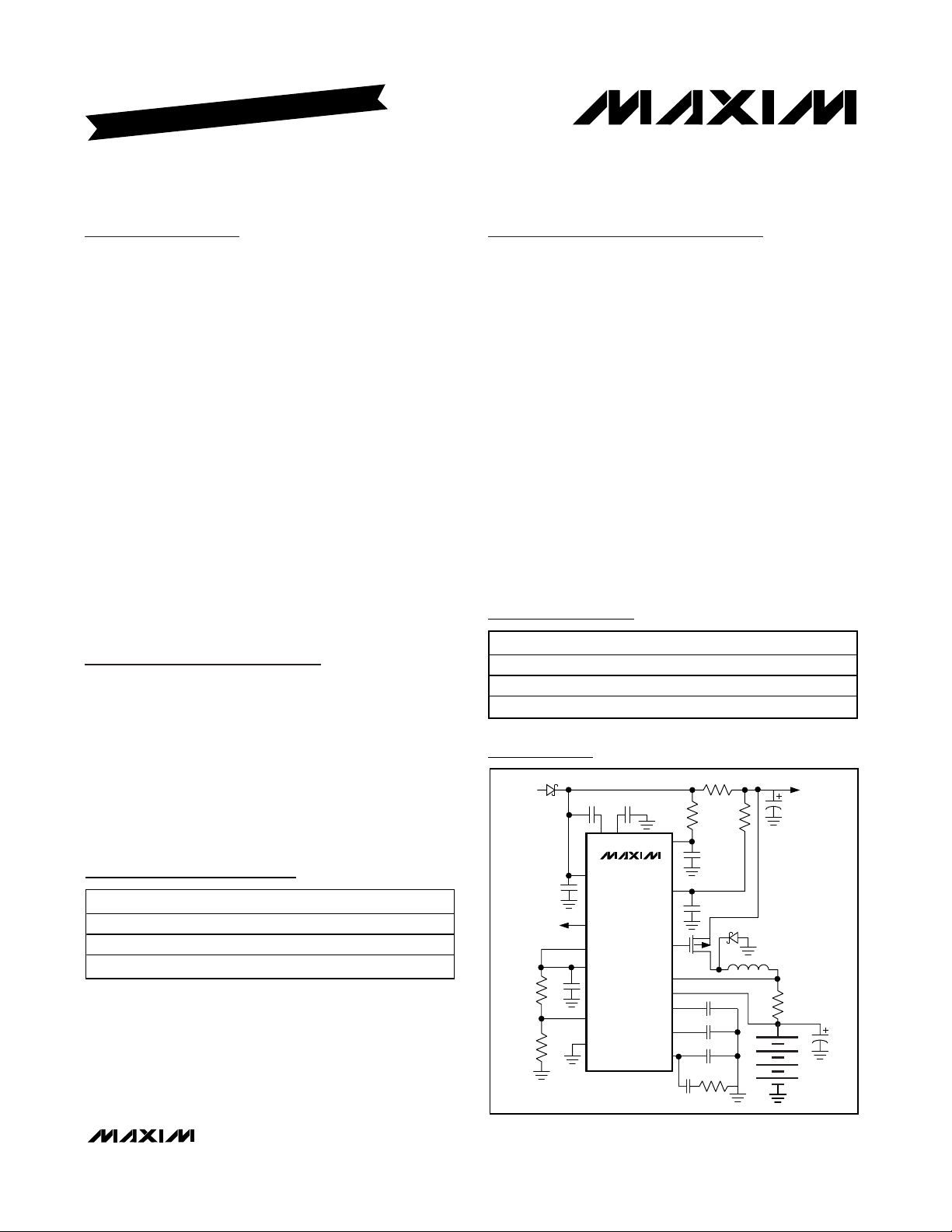
Typical Operating Circuit
Pin Configuration appears at end of data sheet.
PART TEMP. RANGE PIN-PACKAGE
MAX1873REEE -40°C to +85°C 16 QSOP
MAX1873SEEE -40°C to +85°C 16 QSOP
MAX1873TEEE -40°C to +85°C 16 QSOP
VIN 9V TO
28V
(9V MIN
FOR 2-
CELLS)
VH VL CSSP
SYSTEM
LOAD
MAX1873
PART SERIES CELLS TO CHARGE
MAX1873REEE
MAX1873SEEE
MAX1873TEEE 4-Cell Li+ 10-cell Ni Battery Packs
2-Cell Li+ or 5- or 6-cell Ni Battery
3-Cell Li+ or 7- or 9-cell Ni Battery
4V OUT PER
200mV ON R
DCIN
IOUT
CS
ICHG/EN
REF
VADJ
GND
CSSN
EXT
CSB
BATT
CCI
CCS
CCV
2- TO 4-CELL
Li+
Page 2
MAX1873
Simple Current-Limited Switch-Mode
Li+ Charger Controller
2 _______________________________________________________________________________________
ABSOLUTE MAXIMUM RATINGS
ELECTRICAL CHARACTERISTICS
(Circuit of Figure 1, V
DCIN
= V
CSSP
= V
CSSN
= 18V, V
ICHG/EN
= V
REF
, V
VADJ
= V
REF
/2. MAX1873R: V
BATT
= V
CSB
= 8.4V;
MAX1873S: V
BATT
= V
CSB
= 12.6V; MAX1873T: V
BATT
= V
CSB
= 16.8V; TA= 0°C to +85°C. Typical values are at TA= +25°C, unless
otherwise noted.)
Stresses beyond those listed under “Absolute Maximum Ratings” may cause permanent damage to the device. These are stress ratings only, and functional
operation of the device at these or any other conditions beyond those indicated in the operational sections of the specifications is not implied. Exposure to
absolute maximum rating conditions for extended periods may affect device reliability.
CSSP, CSSN, DCIN to GND ...................................-0.3V to +30V
VL, ICHG/EN to GND................................................-0.3V to +6V
VH, EXT to DCIN.......................................................-6V to +0.3V
VH, EXT to GND ......................................(V
DCIN
+ 0.3V) to -0.3V
EXT to VH .................................................................+6V to -0.3V
DCIN to VL..............................................................+30V to -0.3V
VADJ, REF, CCI, CCV, CCS,
IOUT to GND.............................................-0.3V to (VL + 0.3V)
BATT, CSB to GND.................................................-0.3V to +20V
CSSP to CSSN.......................................................-0.3V to +0.6V
CSB to BATT..........................................................-0.3V to +0.6V
VL Source Current ............................................................+50mA
VH Sink Current ................................................................+40mA
Continuous Power Dissipation (T
A
= +70°C)
16-Pin QSOP (derate 8.3mW/°C above +70°C..........+667mW
Operating Temperature Range
MAX1873_EEE................................................-40°C to +85°C
Junction Temperature..................................................... +150°C
Storage Temperature Range .............................-65°C to +150°C
Lead Temperature (soldering, 10s) ................................ +300°C
INPUT SUPPLY AND REFERENCE
DCIN Input Voltage Range 628V
D C IN Qui escent S up p l y C ur r ent
DCIN to BATT Undervoltage Threshold CSSP = DCIN, input falling 0.05 0.175 V
DCIN to BATT Undervoltage Threshold CSSP = DCIN, input rising 0.22 0.38 V
VL Output Voltage 6.0V < V
VL Output Load Regulation IVL = 0 to 3mA 15 50 mV
REF Output Voltage I
REF Line Regulation 6.0V < V
REF Load Regulation I
SWITCHING REGULATOR
PWM Oscillator Frequency 270 300 330 kHz
EXT Driver Source On-Resistance 47Ω
EXT Driver Sink On-Resistance 2.5 4.5 Ω
VH Output Voltage DCIN - VH, 6V < V
CSSN/CSSP Input Current V
CSSN/CSSP Off-State Leakage V
BATT, CSB Input Current
BATT, CSB Input Current DCIN ≤ BATT (input power removed) 1.5 5 µA
PARAMETER CONDITIONS MIN TYP MAX UNITS
6.0V < V
DCIN ≤ BATT 0.1 10 µA
= 21µA (200kΩ load) 4.179 4.20 4.221 V
REF
= 0 to 1mA 6 13 mV
REF
CSSN/VCSSP
DCIN
ICHG/EN = 0 (charger disabled) 0.2 1
ICHG/EN = REF (charger enabled) 250 500
< 28V 4 7 mA
DCIN
< 28V 5.15 5.40 5.65 V
DCIN
< 28V
DCIN
= 28V, V
= V
SSN/VCSSP
<28V, IVH = 0 to 20mA 4.75 5.75 V
DCIN
= 28V 70 200 µA
DCIN
= 18V, V
BATT
= V
= 18V 1.5 5 µA
CSB
26mV
22 65 ppm/V
µA
Page 3
MAX1873
Simple Current-Limited Switch-Mode
Li+ Charger Controller
_______________________________________________________________________________________ 3
ELECTRICAL CHARACTERISTICS (continued)
(Circuit of Figure 1, V
DCIN
= V
CSSP
= V
CSSN
= 18V, V
ICHG/EN
= V
REF
, V
VADJ
= V
REF
/2. MAX1873R: V
BATT
= V
CSB
= 8.4V;
MAX1873S: V
BATT
= V
CSB
= 12.6V; MAX1873T: V
BATT
= V
CSB
= 16.8V; TA= 0°C to +85°C. Typical values are at TA= +25°C, unless
otherwise noted.)
PARAMETER CONDITIONS MIN TYP MAX UNITS
Battery Regulation Voltage
BATT Undervoltage Threshold
CURRENT SENSE
CSB to BATT Battery Current-Sense
Voltage
CSB to BATT Current-Sense Voltage
when V
< 2.5V per Cell
BATT
CSSP to CSSN Current-Sense Voltage 6V < V
CONTROL INPUTS/OUTPUTS
ICHG/EN Input Threshold Includes 50mV of hysteresis 500 600 700 mV
ICHG/EN Input Voltage Range For
Charge Current Adjustment
VADJ Input Current V
ICHG/EN Input Current V
VADJ Input Voltage Range 0V
IOUT Voltage
2-cell version MAX1873R 10.45 11 11.55
3-cell version MAX1873S 15.675 16.5 17.325BATT Overvoltage Cutoff Threshold
4-cell version MAX1873T (Note 1) 17.575 18.5 19.425
V
= 0 7.898 7.958 8.018
MAX1873R
(2 Li+ cells)
MAX1873S
(3 Li+ cells)
MAX1873T
(4 Li+ cells)
VADJ
V
= V
/2 8.337 8.4 8.463
REF
= V
(Note 1) 8.775 8.842 8.909
REF
= 0 11.847 11.937 12.027
= V
/2 12.505 12.6 12.695
REF
= V
(Note 1) 13.163 13.263 13.363
REF
= 0 15.796 15.916 16.036
= V
/2 16.674 16.8 16.926
REF
= V
(Note 1) 17.551 17.684 17.817
REF
V
V
V
V
V
V
V
VADJ
VADJ
VADJ
VADJ
VADJ
VADJ
VADJ
VADJ
MAX1873R 4.8 5.0 5.2
For I
charge
V
V
CHG
ICHG/EN
ICHG/EN
/20 trickle
MAX1873S 7.2 7.5 7.8
MAX1873T 9.6 10 10.4
= V
REF
= V
/4 40 50 60
REF
190 200 210
51015mV
< 28V 90 100 110 mV
CSSP
700 V
= V
VADJ
ICHG/EN
Full scale
25% scale
Trickle charge V
No charge
current
/2 -100 100 nA
REF
= V
REF
V
- V
CSB
0 < I
OUT
V
- V
CSB
0 < I
OUT
- V
CSB
- V
V
CSB
= sinking 20µA
I
IOUT
= 200mV,
BATT
< 500µA
= 50mV,
BATT
< 500µA
= 10mV 75 200 325
BATT
= 0,
BATT
-100 100 nA
3.6 4.0 4.4
0.9 1.0 1.1
40 70 90
REF
REF
mV
mV
mV
V
V
V
V
V
Page 4

MAX1873
Simple Current-Limited Switch-Mode
Li+ Charger Controller
4 _______________________________________________________________________________________
ELECTRICAL CHARACTERISTICS
(Circuit of Figure 1, V
DCIN
= V
CSSP
= V
CSSN
= 18V, V
ICHG/EN
= V
REF
, V
VADJ
= V
REF
/2. MAX1873R: V
BATT
= V
CSB
= 8.4V;
MAX1873S: V
BATT
= V
CSB
= 12.6V; MAX1873T: V
BATT
= V
CSB
= 16.8V; TA= -40°C to +85°C. Typical values are at TA= +25°C,
unless otherwise noted.)
PARAMETER CONDITIONS MIN MAX UNITS
INPUT SUPPLY AND REFERENCE
DCIN Input Voltage Range 628V
D C IN Qui escent S up p l y C ur r ent
DCIN to BATT Undervoltage Threshold CSSP = DCIN, input falling 0.05 0.2 V
DCIN to BATT Undervoltage Threshold CSSP = DCIN, input rising 0.22 0.38 V
VL Output Voltage 6.0V < V
VL Output Load Regulation IVL = 0 to 3mA 50 mV
REF Output Voltage I
REF Line Regulation 6.0V < V
REF Load Regulation I
SWITCHING REGULATOR
PWM Oscillator Frequency 270 330 kHz
EXT Driver Source On-Resistance 7 Ω
EXT Driver Sink On-Resistance 4.5 Ω
VH Output Voltage DCIN - VH, 6V < V
CSSN/CSSP Input Current V
CSSN/CSSP Off-State Leakage V
BATT, CSB Input Current
BATT, CSB Input Current DCIN ≤ BATT (input power removed) 5 µA
BATT Overvoltage Cutoff Threshold
Battery Regulation Voltage
6.0V < V
< 28V 7 mA
DCIN
DCIN ≤ BATT 10 µA
< 28V 5.15 5.65 V
DCIN
= 21µA (200kΩ load) 4.179 4.221 V
REF
< 28V
DCIN
= 0 to 1mA 13 mV
REF
<28V, IVH = 0 to 20mA 4.75 5.75 V
DCIN
CSSN/VCSSP
= V
DCIN
SSN/VCSSP
= 28V, V
= 28V 200 µA
DCIN
= 18V V
BATT
= V
= 18V 5 µA
CSB
6mV
65 ppm/V
ICHG/EN = 0 (charger disabled) 1
ICHG/EN = REF (charger enabled) 500
2-cell version MAX1873R 10.45 11.55
3-cell version MAX1873S 15.675 17.325
4-cell version MAX1873T (Note 1) 17.575 19.425
V
= 0 7.898 8.018
MAX1873R
(2 Li+ cells)
MAX1873S
(3 Li+ cells)
MAX1873T
(4 Li+ cells)
VADJ
V
= V
/2 8.337 8.463
REF
= V
(Note 1) 8.775 8.909
REF
= 0 11.847 12.027
= V
/2 12.505 12.695
REF
= V
(Note 1) 13.163 13.363
REF
= 0 15.796 16.036
= V
/2 16.674 16.926
REF
= V
(Note 1) 17.551 17.817
REF
V
V
V
V
V
V
V
VADJ
VADJ
VADJ
VADJ
VADJ
VADJ
VADJ
VADJ
µA
V
V
Page 5
MAX1873
Simple Current-Limited Switch-Mode
Li+ Charger Controller
_______________________________________________________________________________________ 5
ELECTRICAL CHARACTERISTICS (continued)
(Circuit of Figure 1, V
DCIN
= V
CSSP
= V
CSSN
= 18V, V
ICHG/EN
= V
REF
, V
VADJ
= V
REF
/2. MAX1873R: V
BATT
= V
CSB
= 8.4V;
MAX1873S: V
BATT
= V
CSB
= 12.6V; MAX1873T: V
BATT
= V
CSB
= 16.8V; TA= -40°C to +85°C. Typical values are at TA= +25°C,
unless otherwise noted.)
Note 1: While it may appear possible to set the Battery Regulation Voltage higher than the Battery Overvoltage Cutoff Threshold, this
cannot happen because both parameters are derived from the same reference and track each other.
Note 2: Specifications to -40°C are guaranteed by design, not production tested.
PARAMETER CONDITIONS MIN MAX UNITS
BATT Undervoltage Threshold
CURRENT SENSE
CSB to BATT Battery Current-Sense
Voltage
CSB to BATT Current-Sense Voltage
when V
< 2.5V per Cell
BATT
CSSP to CSSN Current-Sense Voltage 6V < V
CONTROL INPUTS/OUTPUTS
ICHG/EN Input Threshold Includes 50mV of hysteresis 500 700 mV
ICHG/EN Input Voltage Range for
Charge Current Adjustment
VADJ Input Current V
ICHG/EN Input Current V
VADJ Input Voltage Range 0V
IOUT Voltage
For I
CHG
/20 trickle
charge
V
V
ICHG/EN
ICHG/EN
CSSP
= V
VADJ
ICHG/EN
= V
= V
< 28V 90 110 mV
REF
= V
Full scale
25% scale
Trickle charge V
No charge
current
MAX1873R 4.8 5.2
MAX1873S 7.2 7.8
MAX1873T 9.6 10.4
REF
/4 40 60 mV
REF
190 210 mV
515mV
700 V
REF
/2 -100 100 nA
REF
V
- V
CSB
0 < I
OUT
- V
V
CSB
0 < I
OUT
- V
CSB
- V
V
CSB
I
= sinking 20µA
IOUT
= 200mV,
BATT
< 500µA
= 50mV,
BATT
< 500µA
= 10mV 75 325
BATT
= 0,
BATT
-100 100 nA
REF
3.6 4.4
0.9 1.1
40 90
mV
mV
V
V
V
Page 6

MAX1873
Simple Current-Limited Switch-Mode
Li+ Charger Controller
6 _______________________________________________________________________________________
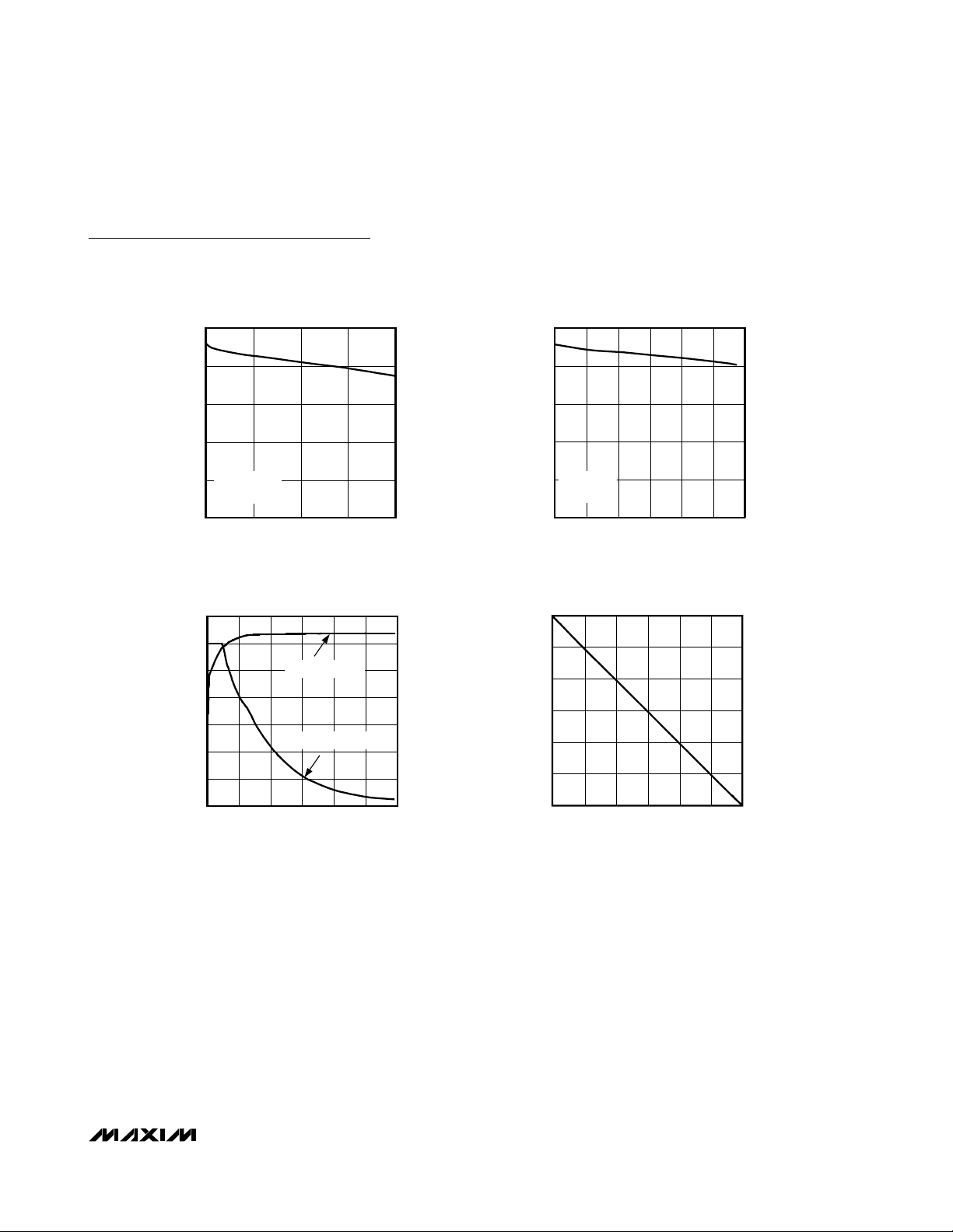
Typical Operating Characteristics
(Circuit of Figure 1, V
DCIN
= V
CSSP
= V
CSSN
= 18V, V
ICHG/EN
= V
REF
, V
VADJ
= V
REF
/2. MAX1873R: V
BATT
= V
CSB
= 8.4V;
MAX1873S: V
BATT
= V
CSB
= 12.6V; MAX1873T: V
BATT
= V
CSB
= 16.8V; TA= +25°C, unless otherwise noted).
0
5.0
2.5
10.0
7.5
15.0
12.5
17.5
0 1.0 1.50.5 2.0 2.5 3.0 3.5
MAX1873T (4-CELL)
BATTERY VOLTAGE vs. CHARGING CURRENT
MAX1873 toc01
CHARGING CURRENT (A)
BATTERY VOLTAGE (V)
R
CSB
+ 0.068Ω
0
1.0
0.5
2.5
2.0
1.5
4.0
3.5
3.0
4.5
010050 150 200 250
IOUT VOLTAGE
vs. CSB-BATT VOLTAGE
MAX1873 toc02
CSB-BATT VOLTAGE (mV)
IOUT VOLTAGE (V)
4.180
4.190
4.185
4.200
4.195
4.205
4.210
RECENT VOLTAGE
VS.
TEMPERATURE
MAX1873 toc04
TEMPERATURE (°C)
REFERENCE VOLTAGE (V)
-50 0 25-25 50 75 100
MAX1873T
15.5
16.0
17.0
16.5
17.5
18.0
021345
MAX1873T (4-CELL)
BATTERY REGULATION VOLTAGE
vs. VADJ VOLTAGE
MAX1873 toc03
VADJ VOLTAGE (V)
BATTERY REGULATION VOLTAGE (V)
4.180
4.195
4.190
4.185
4.200
4.205
4.210
0 0.40.30.1 0.2 0.5 0.6 0.7 0.8 0.9 1.0
RECENT VOLTAGE
VS. REFERENCE CURRENT
MAX1873 toc05
REFERENCE VOLTAGE (mA)
REFERENCE VOLTAGE (V)
MAX1873T
50
60
80
70
90
100
81612 20 24 28
MAX1873R (2-CELL)
EFFICIENCY vs. INPUT VOLTAGE
MAX1873 toc06
INPUT VOLTAGE (V)
EFFICIENCY (%)
V
BATT
= 7V
I
CHG
= 3A
Page 7
MAX1873
Simple Current-Limited Switch-Mode
Li+ Charger Controller
_______________________________________________________________________________________ 7
Typical Operating Characteristics (continued)
(Circuit of Figure 1, V
DCIN
= V
CSSP
= V
CSSN
= 18V, V
ICHG/EN
= V
REF
, V
VADJ
= V
REF
/2. MAX1873R: V
BATT
= V
CSB
= 8.4V;
MAX1873S: V
BATT
= V
CSB
= 12.6V; MAX1873T: V
BATT
= V
CSB
= 16.8V; TA= +25°C, unless otherwise noted).
100
90
80
70
EFFICIENCY (%)
60
50
18
16
14
12
10
BATTERY VOLTAGE (V)
8
6
EFFICIENCY vs. INPUT VOLTAGE
V
= 10.5V
BATT
= 3A
I
CHG
12 2016 24 28
4-CELL BATTERY VOLTAGE AND
CHARGING CURRENT vs. TIME
MAX1873S (3-CELL)
INPUT VOLTAGE (V)
BATTERY VOLTAGE
CHARGING CURRENT
MAX1873 toc07
3.5
3.0
MAX1873 toc09
2.5
2.0
1.5
1.0
0.5
MAX1873T (4-CELL)
EFFICIENCY vs. INPUT VOLTAGE
100
90
80
70
EFFICIENCY (%)
60
V
= 14V
BATT
+ 3A
I
CHG
50
16 2018 22 24 26 28
INPUT VOLTAGE (V)
CHARGING CURRENT
vs. SYSTEM LOAD CURRENT
3.0
2.5
2.0
1.5
1.0
CHARGING CURRENT (A)
CHARGING CURRENT (A)
0.5
MAX1873 toc08
MAX1873 toc10
4
0507525 100 125 150
TIME (MINUTES)
0
0
0 1.0 1.50.5 2.0 2.5 3.0
SYSTEM LOAD CURRENT (A)
Page 8

MAX1873
Simple Current-Limited Switch-Mode
Li+ Charger Controller
8 _______________________________________________________________________________________
Pin Description
PIN NAME FUNCTION
1 CSSN
2 CSSP Source Current-Sense Positive Input. Also used for input source undervoltage sensing.
3 CCS Input-Source-Current Regulation Loop Compensation Point
4 CCV
5 CCI Battery Charge Current Control-Loop Compensation Point
6 ICHG/EN
7 IOUT
8 VADJ
9 REF 4.2V Reference Voltage Output. Bypass to GND with a 1µF ceramic capacitor.
10 BATT
11 CSB Battery Current-Sense Positive Input
12 GND Ground
13 VH
14 EXT Drive Output for External PFET. EXT swings from V
15 DCIN
16 VL
Source Current-Sense Negative Input. Connect a current-sense resistor between CSSP and CSSN to
limit total current drawn from the input source. To disable input current sensing, connect CSSN to CSSP.
Battery Regulation Voltage Control-Loop Compensation Point. Pulling CCV high (to VL) through a 1.5kΩ
resistor disables the voltage control loop for charging NiCd or NiMH batteries.
Battery Charging Current Adjust/Shutdown Input. This pin can be connected to a resistive-divider
between REF and GND to adjust the charge current sense threshold between CSB and BATT. When
ICHG/EN is connected to REF, the CSB-BATT threshold is 200mV. Pull ICHG/EN low (below 500mV) to
disable charging and reduce the supply current to 5µA.
Charge Current Monitor Output. Analog Voltage Output that is proportional to charging current. V
= 20 (V
Battery Regulation Voltage Adjust. Set the battery regulation voltage from 3.979V per cell to 4.421V per
cell with 1% resistors. Output accuracy remains better than 0.75% even with 1% adjusting resistors
due to reduced adjustment range. For 4.2V, the voltage-divider resistors must be equal value
(nominally 100kΩ each).
Battery Voltage-Sense Input and Battery Current-Sense Negative Input. Bypass to GND with a 68µF for
MAX1873R, 47µF for MAX1873S, and 33µF for MAX1873T. Use capacitors with ESR < 1Ω.
Internal VH Regulator. VH internally supplies power to the EXT driver. Connect a 0.22µF ceramic
capacitor between VH and DCIN.
Power-Supply Input. DCIN is the input supply for charger IC. Bypass to GND with a 0.22µF ceramic
capacitor.
Internal VL Regulator. VL powers the MAX1873’s control logic at 5.4V. Bypass to GND with a 2.2µF or
larger ceramic capacitor.
CSB
- V
) or 4V for a 200mV current-sense voltage (maximum load capacitance = 5nF).
BATT
DCIN
to V
DCIN
- 5V.
IOUT
Page 9

Detailed Description
The MAX1873 includes all of the functions necessary to
charge 2-, 3-, or 4-series cell lithium-ion (Li+) battery
packs. It includes a high-efficiency step-down DC-DC
converter that controls charging voltage and current. It
also features input source current limiting so that an AC
adapter that supplies less than the total system current
in addition to charging current can be used without fear
of overload.
The DC-DC converter uses an external P-channel MOSFET switch, inductor, and diode to convert the input voltage to charging current or charging voltage. The typical
application circuit is shown in Figure 1. Charging current
is set by R
CSB
, while the battery voltage is measured at
BATT. The battery regulation voltage limit is nominally
set to 8.4V for the R version (2-cells), 12.6V for the S
version (3-cells), and 16.8V for the T version (4-cells),
but it can also be adjusted to other voltages for different Li+ chemistries.
Voltage Regulator
Li+ batteries require a high-accuracy voltage limit while
charging. The battery regulation voltage is nominally
set to 4.2V per cell and can be adjusted ±5.25% by
setting the voltage at VADJ between REF and ground.
By limiting the adjust range of the regulation voltage, an
overall voltage accuracy of better than ±0.75% is maintained while using 1% resistors.
An internal error amplifier maintains voltage regulation
to within ±0.75%. The amplifier is compensated at CCV
(see Figure 1). Individual compensation of the voltage
regulation and current regulation loops allows for optimal compensation of each. A typical CCV compensation network is shown in Figure 1 and will suffice for
most designs.
MAX1873
Simple Current-Limited Switch-Mode
Li+ Charger Controller
_______________________________________________________________________________________ 9
DISABLE
Figure 1. Typical Application Circuit
VIN 17V TO 28V
(9V MIN FOR 2- CELLS)
N
100kΩ
D1
MBR5340
C
VL
2.2µF
R
C
0.01µF
C
0.01µF
C
REF
1µF
4.7Ω
P
R
4.7Ω
N
P
R
CSS
0.033Ω
N
D2
MBR5340
P
L1
10µH
R1
R2
R
CSB
0.068Ω
C
L
47µF
C
BATT
68µF
BATTERY
(2- TO 4-CELLS)
SYSTEM
LOAD
LI+
C
DCIN
0.22µF
4V OUT PER
200mV ON R
C
CCVS
0.1µF
C
47nF
C
CCS
47nF
R
10kΩ
CSB
CC
CCV
C
VH
0.22µF
VH
DCIN
MAX1873
IOUT
ICHG/EN
CCI
CCS
CCV
CSSP
VL
CSSN
EXT
CSB
BATT
REF
VADJ
GND
C
CCVP
1nF
Page 10

MAX1873
Charging-Current Regulator
The charging-current regulator limits the battery charging current. Current is sensed by the current-sense
resistor (R
CSB
in Figure 1) connected between BATT
and CSB. The voltage on ICHG/EN can also adjust the
charging current. Full-scale charging current (I
CHG
=
0.2V / RCSB) is achieved by connecting ICHG/EN to
REF. See Setting the Charging-Current Limit section for
more details.
The charging-current error amplifier is compensated at
CCI (Figure 1). A 47nF capacitor from CCI to GND provides suitable performance for most applications.
Input-Current Regulator
The input-current regulator limits the source current by
reducing charging current when the input current
reaches the set input-current limit. In a typical portable
design, system load current will normally fluctuate as
portions of the system are powered up or put to sleep.
Without the benefit of input-current regulation, the input
source would have to be able to supply the maximum
system current plus the maximum charger-input current. The MAX1873 input-current loop ensures that the
system always gets adequate power by reducing
charging current as needed. By using the input-current
limiter, the size and cost of the AC adapter can be
reduced. See Setting the Input-Current Limit section for
design details.
Input current is measured through an external sense
resistor, R
CSS
, between CSSP and CSSN. The inputcurrent limit feature may be bypassed by connecting
CSSP to CSSN.
The input-current error amplifier is compensated at
CCS. A 47nF capacitor from CCS to GND provides suitable performance for most applications.
PWM Controller
The pulse-width modulation (PWM) controller drives the
external MOSFET at a constant 300kHz to regulate the
charging current and voltage while maintaining low
noise. The controller accepts inputs from the CCI, CCV,
and CCS error amplifiers. The lowest signal of these
three drives the PWM controller. An internal clamp limits
the noncontrolling signals to within 200mV of the controlling signal to prevent delay when switching between
the battery-voltage control, charging-current control,
and input-current regulation loops.
Shutdown
The MAX1873 stops charging when ICHG/EN is pulled
low (below 0.5V) and shuts down when the voltage at
DCIN falls below the voltage at BATT. In shutdown, the
internal resistive voltage-divider is disconnected from
BATT to reduce the battery drain. When AC-adapter
power is removed, or when the part is shut down, the
MAX1873 typically draws 1.5µA from the battery.
Source Undervoltage Shutdown (Dropout)
The DCIN voltage is compared to the voltage at BATT.
When the voltage at DCIN drops below BATT + 50mV,
the charger turns off, preventing drain on the battery
when the input source is not present or is below the
battery voltage.
A diode is typically connected between the input
source and the charger input. This diode prevents the
battery from discharging through the body diode of the
high-side MOSFET should the input be shorted to GND.
It also protects the charger, battery, and systems from
reversed polarity adapters and negative input voltages.
Simple Current-Limited Switch-Mode
Li+ Charger Controller
10 ______________________________________________________________________________________
Figure 2. Functional Block Diagram
CSSN
CSSP
CCS
CCV
CCI
ICHG
/EN
IOUT
9R
VADJ
A = 1
GND
SHUTDOWN
FOR ALL
BLOCKS
CONTROL
LOGIC
CURRENT
ERROR AMP
R
5.4
REGULATOR
UNDERVOLTAGE
COMPARATOR
BATT
VH
DRIVER
VOLTAGE
ERROR AMP
R
4.2V
REFERENCE
VL
DCIN
EXT
VH
GND
CSB
BATT
REF
Page 11

Charge-Current Monitor Output
IOUT is an analog voltage output that is proportional to
the actual charge current. With the aid of a microcontroller, the IOUT signal can facilitate gas-gauging, indicate percent of charge, or charge-time remaining. The
equation governing this output is:
where V
CSB
and V
BATT
are the voltages at the CSB and
BATT pins, and ICHG is the charging current. IOUT can
drive a load capacitance of 5nF.
Design Procedure
Setting the Battery-Regulation Voltage
For Li+ batteries, VADJ sets the per-cell battery-regulation voltage limit. To set the VADJ voltage, use a resistive-divider from REF to GND (Figure 1). For a battery
voltage of 4.2V per cell, use resistors of equal value
(100kΩ each) in the VADJ voltage-divider. To set other
battery-regulation voltages, see the remainder of this
section.
The per-cell battery regulation voltage is a function of
Li+ battery chemistry and construction and is usually
clearly specified by the manufacturer. If this is not
clearly specified, be sure to consult the battery manufacturer to determine this voltage before charging any
Li+ battery. Once the per-cell voltage is determined,
the VADJ voltage is calculated by the equation:
where V
BATTR
is the desired battery-regulation voltage
(for the total series-cell stack), N is the number of Li+
battery cells, and V
REF
is the reference voltage (4.2V).
Set V
VADJ
by choosing R1. R1 should be selected so
that the total divider resistance (R1+ R2) is near 200kΩ.
R2 can then be calculated as follows:
Since the full range of VADJ (from 0 to VREF) results in
a ±5.263% adjustment of the battery-regulation limit
(3.979V to 4.421V), the resistive-divider’s accuracy
need not be as tight as the output-voltage accuracy.
Using 1% resistors for the voltage-divider still provides
±0.75% battery-voltage-regulation accuracy.
Setting the Charging-Current Limit
The charging current ICHG is sensed by the currentsense resistor R
CSB
between CSB and BATT, and is
also adjusted by the voltage at ICHG/EN. If ICHG/EN is
connected to REF (the standard connection), the
charge current is given by:
In some cases, common values for R
CSB
may not allow
the desired charge-current value. It may also be desirable to reduce the 0.2V CSB-to-BATT sense threshold
to reduce power dissipation. In such cases, the
ICHG/EN input may be used to reduce the charge-current-sense threshold. In those cases the equation for
charge current becomes:
Setting the Input-Current Limit
The input-source current limit, IIN, is set by the inputcurrent sense resistor, R
CSS
, (Figure 1) connected
between CSSP and CSSN. The equation for the source
current is:
This limit is typically set to the current rating of the input
power source or AC adapter to protect the input source
from overload. Short CSSP and CSSN to DCIN if the
input-source current-limit feature is not used.
Inductor Selection
The inductor value may be selected for more or less
ripple current. The greater the inductance, the lower
the ripple current. However, as the physical size is kept
the same, larger inductance value typically results in
higher inductor series resistance and lower inductor
saturation current. Typically, a good tradeoff is to
choose the inductor such that the ripple current is
approximately 30% to 50% of the DC average charging
current. The ratio of ripple current to DC charging current (LIR) can be used to calculate the inductor value:
where f
SW
is the switching frequency (nominally
300kHz) and I
CHG
is the charging current. The peak
inductor current is given by:
MAX1873
Simple Current-Limited Switch-Mode
Li+ Charger Controller
______________________________________________________________________________________ 11
VVVor
=−
20
IOUT CSB BATT
VRI
OUT CSB CHG
()
=×
20
()
VVNV
=
95 9./
()
VADJ BATTR REF
RV V V R
[]
21=−
[]
()
VADJ REF VADJ
−
()
×/
IVVVR
CHG ICH EN REF CSB
IVR
= 02./
CHG CSB
=
02.//
()
/
IVR
= 01./
IN CSS
LV V V
=−
BATT DCIN MAX BATT
[]
{}
VfILIR
DCIN MAX SW CHG
()
[]
()
×× ×
/
Page 12
MAX1873
For example, for a 4-cell charging current of 3A, a
V
DCIN(MAX)
of 24V, and an LIR of 0.5, L is calculated to
be 11.2µH with a peak current of 3.75A. Therefore a
10µH inductor would be satisfactory.
MOSFET Selection
The MAX1873 uses a P-channel power MOSFET
switch. The MOSFET must be selected to meet the efficiency or power dissipation requirements of the charging circuit as well as the maximum temperature of the
MOSFET. Characteristics that affect MOSFET power
dissipation are drain-source on-resistance (
RDS(ON)
)
and gate charge. Generally these are inversely proportional.
To determine MOSFET power dissipation, the operating
duty cycle must first be calculated. When the charger is
operating at higher currents, the inductor current will be
continuous (the inductor current will not drop to 0). In
this case, the high-side MOSFET duty cycle (D) can be
approximated by the equation:
And the catch-diode duty cycle (D') will be 1 - D or:
where V
BATT
is the battery-regulation voltage (typically
4.2V per cell) and V
DCIN
is the source-input voltage.
For MOSFETs, the worst-case power dissipation due to
on-resistance (PR) occurs at the maximum duty cycle,
where the operating conditions are minimum sourcevoltage and maximum battery voltage. PRcan be
approximated by the equation:
Transition losses (PT) can be approximated by the
equation:
where tTRis the MOSFET transition time and fSWis the
switching frequency. The total power dissipation of the
MOSFET is then:
Diode Selection
A Schottky rectifier with a current rating of at least the
charge current limit must be connected from the MOSFET drain to GND. The voltage rating of the diode must
exceed the maximum expected input voltage.
Capacitor Selection
The input capacitor shunts the switching current from
the charger input and prevents that current from circulating through the source, typically an AC wall cube.
Thus the input capacitor must be able to handle the
input RMS current. At high charging currents, the converter will typically operate in continuous conduction. In
this case, the RMS current of the input capacitor can
be approximated with the equation:
where I
CIN
is the input capacitor RMS current, D is the
PWM converter duty cycle (typically V
BATT/VDCIN
), and
I
CHG
is the battery-charging current.
The maximum RMS input current occurs at 50% duty
cycle, so the worst-case input-ripple current is 0.5 x
I
CHG
. If the input-to-output voltage ratio is such that the
PWM controller will never work at 50% duty cycle, then
the worst-case capacitor current will occur where the
duty cycle is nearest 50%.
The impedance of the input capacitor is critical to preventing AC currents from flowing back into the wall
cube. This requirement varies depending on the wall
cube’s impedance and the requirements of any conducted or radiated EMI specifications that must be met.
Low ESR aluminum electrolytic capacitors may be
used, however, tantalum or high-value ceramic capacitors generally provide better performance.
The output filter capacitor absorbs the inductor-ripple
current. The output-capacitor impedance must be significantly less than that of the battery to ensure that it
will absorb the ripple current. Both the capacitance and
the ESR rating of the capacitor are important for its
effectiveness as a filter and to ensure stability of the
PWM circuit. The minimum output capacitance for stability is:
Simple Current-Limited Switch-Mode
Li+ Charger Controller
12 ______________________________________________________________________________________
PPP
II LIR
=+
PEAK CHG
12/
()
=+
TOT R T
V
BATT
D
≈
V
DCIN
VV
−
DCIN BATT
D
'≈
V
DCIN
V
BATT MAX
P
=××
R
()
V
DCIN MIN
()
RI
DS ON CHG
()
2
VIft
×××
DCIN CHG SW TR
P
=
T
3
II DD
≈−
CIN CHG
2
C
V
REF
>
OUT
VfR
BATT SW CSB
V
+
1
V
DCIN MIN
××
BATT
()
Page 13

where C
OUT
is the total output capacitance, V
REF
is the
reference voltage (4.2V), V
BATT
is the maximum battery
regulation voltage (typically 4.2V per cell), V
DCIN (MIN)
is the minimum source-input voltage, and R
CSB
is the
current-sense resistor (68mΩ for 3A charging current)
from CSB to BATT.
The maximum output capacitor ESR allowed for stability is:
where R
ESR
is the output capacitor ESR.
Compensation Components
The three regulation loops: input current limit, charging
current limit, and charging voltage limit are compensated separately using the CCS, CCI, and CCV pins,
respectively.
The charge-current loop error-amplifier output is
brought out at CCI. Likewise, the source-current erroramplifier output is brought out at CCS. 47nF capacitors
to ground at CCI and CCS compensate the current
loops in most charger designs. Raising the value of
these capacitors reduces the bandwidth of these loops.
The voltage-regulating loop error-amplifier output is
brought out at CCV. Compensate this loop by connecting a capacitor in parallel with a series resistor-capacitor from CCV to GND. Recommended values are shown
in Figure 1.
Applications Information
VL, VH, and REF Bypassing
The MAX1873 uses two internal linear regulators to
power internal circuitry. The outputs of the linear regulators are at VL and VH. VL powers the internal control
circuitry while VH powers the MOSFET gate driver. VL
may also power a limited amount of external circuitry,
as long as its maximum current (3mA) is not exceeded.
A 2.2µF bypass capacitor is required from VL to GND
to ensure stability. A 0.22µF capacitor is required from
VH to DCIN. A 1µF bypass capacitor is required
between REF and GND to ensure that the internal 4.2V
reference is stable. In all cases, use low-ESR ceramic
capacitors.
Charging NiMH and NiCd Cells
The MAX1873 may be used in multichemistry chargers.
When charging NiMH or NiCd cells, pull CCV high (to
VL) with a 1.5 kΩ resistor. This disables the voltage
control loop so the Li+ battery-regulation voltage set-
tings do not interfere with charging. However, the battery undervoltage-protection features remain active so
charging current is reduced when V
BATT
is less than
the levels stated in the BATT Undervoltage Threshold
line in the Electrical Characteristics Table. 5- or 6-series
Ni cells may be charged with the R version device, 7to 9-cells with the S version, and 10-cells with the T version.
The MAX1873 contains no charge-termination algorithms for Ni cells; it acts only as a current source. A
separate microcontroller or Ni-cell charge controller
must instruct the MAX1873 to terminate charging.
Chip Information
PROCESS: BiCMOS
TRANSISTOR COUNT: 1397
MAX1873
Simple Current-Limited Switch-Mode
Li+ Charger Controller
______________________________________________________________________________________ 13
Pin Configuration
RV
×
CSB BATT
<
V
REF
R
ESR
TOP VIEW
1
CSSN VL
CSSP
2
CCS
3
MAX1873R/S/T
4
CCV
CCI
5
ICHG/EN
6
IOUT
7
VADJ
8
16 QSOP
16
15
DCIN
14
EXT
13
VH
12
GND
CSB
11
10
BATT
9
REF
Page 14

MAX1873
Simple Current-Limited Switch-Mode
Li+ Charger Controller
Maxim cannot assume responsibility for use of any circuitry other than circuitry entirely embodied in a Maxim product. No circuit patent licenses are
implied. Maxim reserves the right to change the circuitry and specifications without notice at any time.
14 ____________________Maxim Integrated Products, 120 San Gabriel Drive, Sunnyvale, CA 94086 408-737-7600
© 2001 Maxim Integrated Products Printed USA is a registered trademark of Maxim Integrated Products.
Package Information
QSOP.EPS
 Loading...