

Page 1
General Description
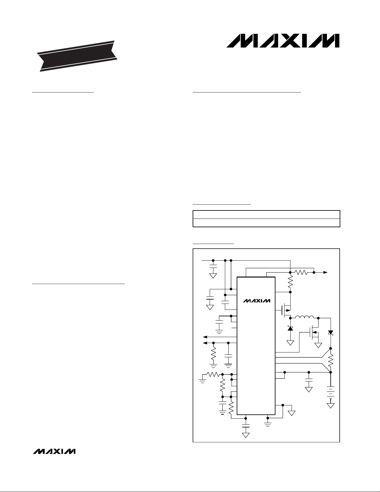
The MAX1870A step-up/step-down multichemistry battery charger charges with battery voltages above and
below the adapter voltage. This highly integrated
charger requires a minimum number of external components. The MAX1870A uses a proprietary step-up/stepdown control scheme that provides efficient charging.
Analog inputs control charge current and voltage, and
can be programmed by the host or hardwired.
The MAX1870A accurately charges two to four lithiumion (Li+) series cells at greater than 4A. A programmable input current limit is included, which avoids
overloading the AC adapter when supplying the load
and the battery charger simultaneously. This reduces
the maximum adapter current, which reduces cost. The
MAX1870A provides analog outputs to monitor the current drawn from the AC adapter and charge current. A
digital output indicates the presence of an AC adapter.
When the adapter is removed, the MAX1870A consumes less than 1µA from the battery.
The MAX1870A is available in a 32-pin thin QFN (5mm
x 5mm) package and is specified over the -40°C to
+85°C extended temperature range. The MAX1870A
evaluation kit (MAX1870AEVKIT) is available to help
reduce design time.
Applications
Notebook and Subnotebook Computers
Hand-Held Terminals
Features
♦ Patented Step-Up/Step-Down Control Scheme*
♦ ±0.5% Charge-Voltage Accuracy
♦ ±9% Charge-Current Accuracy
♦ ±8% Input Current-Limit Accuracy
♦ Programmable Maximum Battery Charge Current
♦ Analog Inputs Control Charge Current, Charge
Voltage, and Input Current Limit
♦ Analog Output Indicates Adapter Current
♦ Input Voltage from 8V to 28V
♦ Battery Voltage from 0 to 17.6V
♦ Charges Li+ or NiCd/NiMH Batteries
♦ Tiny 32-Pin Thin QFN (5mm x 5mm) Package
MAX1870A
Step-Up/Step-Down
Li+ Battery Charger
________________________________________________________________ Maxim Integrated Products 1
Ordering Information
MAX1870A
REFIN
DCIN
CSSP
CSSN
DHI
DBST
CSIP
CSIN
BATT
SHDN
ASNS
VCTL
IINP
PGND
SYSTEM
LOAD
N
P
GND
ICTL
CLS
CELLS
FROM WALL ADAPTER
CSSS
VHN
VHP
BLKP
REF
LDO
DLOV
Typical Operating Circuit
19-3243; Rev 0; 4/04
For pricing, delivery, and ordering information, please contact Maxim/Dallas Direct! at
1-888-629-4642, or visit Maxim’s website at www.maxim-ic.com.
EVALUATION KIT
AVAILABLE
Pin Configuration appears at end of data sheet.
PART TEMP RANGE PIN-PACKAGE
MAX1870AETJ
-40°C to +85°C 32 Thin QFN
*Protected by U.S. Patent No. 6,087,816.
Page 2
MAX1870A
Step-Up/Step-Down
Li+ Battery Charger
2 _______________________________________________________________________________________
ABSOLUTE MAXIMUM RATINGS
ELECTRICAL CHARACTERISTICS
(Circuit of Figure 2, V
DCIN
= V
CSSP
= V
CSSN
= V
CSSS
= V
VHP
= 18V, V
BATT
= V
CSIP
= V
CSIN
= V
BLKP
= 12V, V
REFIN
= 3.0V, V
ICTL
=
0.75 x V
REFIN
, VCTL = LDO, CELLS = FLOAT, GND = PGND = 0, V
DLOV
= 5.4V, TA= 0°C to +85°C, unless otherwise noted. Typical
values are at T
A
= +25°C.)
Stresses beyond those listed under “Absolute Maximum Ratings” may cause permanent damage to the device. These are stress ratings only, and functional
operation of the device at these or any other conditions beyond those indicated in the operational sections of the specifications is not implied. Exposure to
absolute maximum rating conditions for extended periods may affect device reliability.
DCIN, CSSP, CSSS, CSSN,
VHP, VHN, DHI to GND......................................-0.3V to +30V
VHP, DHI to VHN .....................................................-0.3V to +6V
BATT, CSIP, CSIN, BLKP to GND ..........................-0.3V to +20V
CSIP to CSIN, CSSP to CSSN,
CSSP to CSSS, PGND to GND..........................-0.3V to +0.3V
CCI, CCS, CCV, REF, IINP to GND ..........-0.3V to (V
LDO
+ 0.3V)
DBST to GND..........................................-0.3V to (V
DLOV
+ 0.3V)
DLOV, VCTL, ICTL, REFIN, CELLS,
CLS, LDO, ASNS,
SHDN to GND.........................-0.3V to +6V
LDO Current........................................................................50mA
Continuous Power Dissipation (T
A
= +70°C)
32-Pin Thin QFN 5mm x 5mm
(derate 21mW/°C above +70°C)......................................1.7W
Operating Temperature Range
MAX1870AETJ.................................................-40°C to +85°C
Storage Temperature Range .............................-60°C to +150°C
Lead Temperature (soldering, 10s) ................................ +300°C
PARAMETER CONDITIONS
MIN
TYP
MAX
UNITS
CHARGE-VOLTAGE REGULATION
VCTL Range 0 3.6 V
V
VCTL
= V
LDO
(2 cells)
V
VCTL
= V
LDO
(3 cells)
V
VCTL
= V
LDO
(4 cells)
V
VCTL
= V
REFIN
(2 cells)
V
VCTL
= V
REFIN
(3 cells)
V
VCTL
= V
REFIN
(4 cells)
V
VCTL
= V
REFIN
/ 20 (2 cells)
V
VCTL
= V
REFIN
/ 20 (3 cells)
Battery Regulation Voltage
Accuracy
V
VCTL
= V
REFIN
/ 20 (4 cells)
%
VCTL Default Threshold VCTL rising 4.0 4.1 4.2 V
0 < V
VCTL
< V
REFIN
-1 +1
DCIN = 0
,
V
REFIN = VVCTL = 3.6V
-1 +1
VCTL Input Bias Current
VCTL = DCIN = 0,
V
REFIN
= 3.6V
-1 +1
µA
CHARGE-CURRENT REGULATION
ICTL Range 0 3.6 V
V
ICTL
= V
REFIN
67 73 79
V
ICTL
= V
REFIN x 0.8
54 59 64
Quick-Charge-Current Accuracy
V
ICTL
= V
REFIN x 0.583
39 43 47
mV
Trickle-Charge-Current Accuracy
V
ICTL
= V
REFIN x 0.0625
3.0 4.5 6.0 mV
BATT/CSIP/CSIN Input Voltage
Range
0 19 V
DCIN = 0 0.1 2
ICTL = 0 0.1 2 CSIP Input Current
ICTL = REFIN
600
µA
-0.5
-0.5
-0.5
-0.8
-0.8
-0.8
-1.2
-1.2
-1.2
+0.5
+0.5
+0.5
+0.8
+0.8
+0.8
+1.2
+1.2
+1.2
350
Page 3
MAX1870A
Step-Up/Step-Down
Li+ Battery Charger
_______________________________________________________________________________________ 3
PARAMETER CONDITIONS
MIN
TYP
MAX
UNITS
DCIN = 0 0.1 2
ICTL = 0 0.1 2 CSIN Input Current
ICTL = REFIN 0.1 2
µA
ICTL Power-Down-Mode
Threshold Voltage
REFIN /
100
REFIN /55 REFIN /
32
V
0 < V
ICTL
< V
REFIN
-1 +1
ICTL Input Bias Current
ICTL = DCIN = 0,
V
REFIN = 3.6V
-1 +1
µA
INPUT-CURRENT REGULATION
CLS = REF 97
113
Charger-Input Current-Limit
Accuracy (V
CSSP
- V
CSSN
)
CSSS = CSSP
CLS = REF x 0.845 81 88 95
mV
CLS = REF 97
113
System-Input Current-Limit
Accuracy (V
CSSP
- V
CSSS
)
CSSN = CSSP
CLS = REF x 0.845 81 88 95
mV
CSSP/CSSS/CSSN Input Voltage
Range
8 28 V
V
CSSP
= V
CSSN
= V
CSSS
= V
DCIN
= 6V -1 +1
CSSP Input Current
V
CSSP
= V
CSSN
= V
CSSS
= V
DCIN
= 8V, 28V
µA
V
CSSP
= V
CSSN
= V
CSSS
= V
DCIN
= 6V -1 +1
CSSS/CSSN Input Current
V
CSSP
= V
CSSN
= V
CSSS
= V
DCIN
= 8V, 28V -1 +1
µA
CLS Input Range
V
CLS Input Bias Current CLS = REF -1 +1 µA
IINP Transconductance V
CSSP
- V
CSSS
= 102mV, CSSN = CSSP 2.5
3.1
µA/mV
V
CSSP
- V
CSSN
= 200mV, V
IINP
= 0V
IINP Output Current
V
CSSP
- V
CSSS
= 200mV, V
IINP
= 0V
µA
V
CSSP
- V
CSSN
= 200mV, IINP float 3.5
IINP Output Voltage
V
CSSP
- V
CSSS
= 200mV, IINP float 3.5
V
SUPPLY AND LINEAR REGULATOR
DCIN Input Voltage Range 8 28 V
DCIN falling 4 6.2
DCIN Undervoltage Lockout
DCIN rising 6.3
V
DCIN Quiescent Current 8.0V < V
DCIN
< 28V 3.5 6 mA
BATT Input Voltage Range 0 19 V
DCIN = 0 0.1 1
BATT Input Bias Current
V
BATT
= 2V to 19V
500
µA
LDO Output Voltage No load 5.3 5.4 5.5 V
LDO Load Regulation 0 < I
LDO
< 10mA 70
mV
LDO Undervoltage Lockout V
DCIN
= 8V, LDO rising
5.0
V
ELECTRICAL CHARACTERISTICS (continued)
(Circuit of Figure 2, V
DCIN
= V
CSSP
= V
CSSN
= V
CSSS
= V
VHP
= 18V, V
BATT
= V
CSIP
= V
CSIN
= V
BLKP
= 12V, V
REFIN
= 3.0V, V
ICTL
=
0.75 x V
REFIN
, VCTL = LDO, CELLS = FLOAT, GND = PGND = 0, V
DLOV
= 5.4V, TA= 0°C to +85°C, unless otherwise noted. Typical
values are at T
A
= +25°C.)
V
REF
350
350
105
105
700 1200
/ 2 V
2.8
REF
7.85
300
150
4.00
5.25
Page 4
MAX1870A
Step-Up/Step-Down
Li+ Battery Charger
4 _______________________________________________________________________________________
PARAMETER CONDITIONS
MIN
TYP
MAX
UNITS
REFERENCE
REF Output Voltage I
REF
= 0µA
V
REF Load Regulation 0 < I
REF
< 500µA 5 10 mV
REF Undervoltage-Lockout Trip
Point
V
REF
falling
3.9 V
REFIN Input Range 2.5 3.6 V
REFIN UVLO Rising
2.2 V
REFIN UVLO Hysteresis 50 mV
V
DCIN
= 18V 50 100
REFIN Input Bias Current
DCIN = 0, V
REFIN
= 3.6V -1 +1
µA
SWITCHING REGULATOR
C ycl e- b y- C ycl e S tep - U p M axi m um
C ur r ent- Li m i t S ense V ol tag e
V
DCIN
= 12V, V
BATT
= 16.8V
135
165 mV
C ycl e- b y- C ycl e S tep - D ow n
M axi m um C ur r ent- Li m i t S ense
V ol tag e
V
DCIN
= 19V, V
BATT
= 16.8V 135
165 mV
Step-Down On-Time V
DCIN
= 18V, V
BATT
= 16.8V 2.2
2.6 µs
Minimum Step-Down Off-Time V
DCIN
= 18V, V
BATT
= 16.8V
µs
Step-Up Off-Time V
DCIN
= 12V, V
BATT
= 16.8V 1.6
2.0 µs
Minimum Step-Up On-Time V
DCIN
= 12V, V
BATT
= 16.8V
µs
MOSFET DRIVERS
VHP - VHN Output Voltage 8V < V
VHP
< 28V, no load 4.5 5 5.5 V
VHN Load Regulation 0 < I
VHN
< 10mA 70 150 mV
DHI On-Resistance High I
SOURCE
= 10mA 2 5 Ω
DHI On-Resistance Low I
SINK
= 10mA 1 3 Ω
DCIN = 0
1 µA
VHP Input Bias Current
V
DCIN
= 18V
2 mA
ICTL = 0
2
BLKP Input Bias Current
V
ICTL
= V
REFIN
= 3.3V
400
µA
DLOV Supply Current DBST low 5 10 µA
DBST On-Resistance High I
SOURCE
= 10mA 2 5 Ω
DBST On-Resistance Low I
SINK
= 10mA 1 3 Ω
ERROR AMPLIFIERS
GMV Amplifier Loop
Transconductance
V C TL = RE FIN , V
BAT T
= 16.8V 0.05
GMI Amplifier Loop
Transconductance
ICTL = REFIN, V
CSIP
- V
CSIN
= 72mV 1.8
3.0
ELECTRICAL CHARACTERISTICS (continued)
(Circuit of Figure 2, V
DCIN
= V
CSSP
= V
CSSN
= V
CSSS
= V
VHP
= 18V, V
BATT
= V
CSIP
= V
CSIN
= V
BLKP
= 12V, V
REFIN
= 3.0V, V
ICTL
=
0.75 x V
REFIN
, VCTL = LDO, CELLS = FLOAT, GND = PGND = 0, V
DLOV
= 5.4V, TA= 0°C to +85°C, unless otherwise noted. Typical
values are at T
A
= +25°C.)
4.076 4.096 4.116
3.1
1.9
150
150
2.4
0.15 0.4 0.50
1.8
0.15 0.3 0.40
0.1
1.3
0.1
100
0.1 0.20 µA/mV
2.4
µA/mV
Page 5
MAX1870A
Step-Up/Step-Down
Li+ Battery Charger
_______________________________________________________________________________________ 5
PARAMETER CONDITIONS
MIN
TYP
MAX
UNITS
V
CLS
= REF, V
CSSP
- V
CSSN
= 102mV, V
CSSP
= V
CSSS
1.2
2.2
GMS Amplifier Loop
Transconductance
V
CLS
= REF, V
CSSP
- V
CSSS
= 102mV, V
CSSP
= V
CSSN
1.2
2.2
VCTL = REFIN, V
BATT
= 15.8V 50
CCV Output Current
VCTL = REFIN, V
BATT
= 17.8V -50
µA
ICTL = REFIN, V
CSIP
- V
CSIN
= 0mV 150
CCI Output Current
ICTL = REFIN, V
CSIP
- V
CSIN
= 150mV
µA
CLS = REF, V
CSSP
= V
CSSN
, V
CSSP
= V
CSSS
100
CCS Output Current
CLS = REF, V
CSSP
- V
CSSN
= 200mV,
V
CSSP
- V
CSSS
= 200mV
µA
CCI/CCS/CCV Clamp Voltage
1.1V < V
CCV
< 3.5V, 1.1V < V
CCS
< 3.5V,
1.1V < V
CCI
< 3.5V
100
500 mV
LOGIC LEVELS
ASNS Output-Voltage Low V
IINP
= GND, I
SINK
= 1mA 0.4 V
ASNS Output-Voltage High V
IINP
= 4V, I
SOURCE
= 1mA
LDO -
0.5
V
V
IINP
rising 1.1
1.2 V
ASNS Current Detect
Hysteresis 50 mV
V
SHDN
= 0 to V
REFIN
-1 +1
SHDN Input Bias Current
DCIN = 0, V
REFIN
= 5V, V
SHDN
= 0 to V
REFIN
-1 +1
µA
SHDN Threshold SHDN falling, V
REFIN
= 2.8V to 3.6V 22
25
% of
SHDN Hysteresis 1
% of
CELLS Input Low Voltage
V
CELLS Float Voltage 40 50 60
% of
CELLS Input High Voltage
RE FIN -
V
CELLS Input Bias Current CELLS = 0 to REFIN -2 +2 µA
ELECTRICAL CHARACTERISTICS (continued)
(Circuit of Figure 2, V
DCIN
= V
CSSP
= V
CSSN
= V
CSSS
= V
VHP
= 18V, V
BATT
= V
CSIP
= V
CSIN
= V
BLKP
= 12V, V
REFIN
= 3.0V, V
ICTL
=
0.75 x V
REFIN
, VCTL = LDO, CELLS = FLOAT, GND = PGND = 0, V
DLOV
= 5.4V, TA= 0°C to +85°C, unless otherwise noted. Typical
values are at T
A
= +25°C.)
1.7
1.7
µA/mV
-150
-100
300
0.75V
1.15
23.5
REFIN
REFIN
0.75
REFIN
Page 6
MAX1870A
Step-Up/Step-Down
Li+ Battery Charger
6 _______________________________________________________________________________________
PARAMETER CONDITIONS
MIN
TYP
MAX
UNITS
CHARGE-VOLTAGE REGULATION
VCTL Range 0 3.6 V
V
VCTL
= V
LDO
(2 cells)
V
VCTL
= V
LDO
(3 cells)
V
VCTL
= V
LDO
(4 cells)
V
VCTL
= V
REFIN
(2 cells)
V
VCTL
= V
REFIN
(3 cells)
V
VCTL
= V
REFIN
(4 cells)
V
VCTL
= V
REFIN
/ 20 (2 cells)
V
VCTL
= V
REFIN
/ 20 (3 cells)
Battery Regulation Voltage
Accuracy
V
VCTL
= V
REFIN
/ 20 (4 cells)
%
VCTL Default Threshold VCTL rising 4.0 4.2 V
CHARGE-CURRENT REGULATION
ICTL Range 0 3.6 V
V
ICTL
= V
REFIN
66 80
V
ICTL
= V
REFIN x 0.8
53 65
Quick-Charge-Current Accuracy
V
ICTL
= V
REFIN x 0.583
38 48
mV
BATT/CSIP/CSIN Input Voltage
Range
0 19 V
CSIP Input Current
µA
ICTL Power-Down-Mode
Threshold Voltage
REFIN /
100
REFIN /
32
V
INPUT-CURRENT REGULATION
CLS = REF 95 115
Charger-Input Current-Limit
Accuracy (V
CSSP
- V
CSSN
)
CSSS = CSSP
CLS = REF x 0.845 79 97
mV
CLS = REF 95 115
System-Input Current-Limit
Accuracy (V
CSSP
- V
CSSS
)
CSSN = CSSP
CLS = REF x 0.845 79 97
mV
CSSP/CSSS/CSSN Input Voltage
Range
8 28 V
CSSP Input Current
µA
CLS Input Range
V
IINP Transconductance V
CSSP
- V
CSSS
= 102mV, CSSN = CSSP 2.5 3.1
µA/mV
V
CSSP
- V
CSSN
= 200mV, V
IINP
= 0V
IINP Output Current
V
CSSP
- V
CSSS
= 200mV, V
IINP
= 0V
µA
V
CSSP
- V
CSSN
= 200mV, IINP float 3.5
IINP Output Voltage
V
CSSP
- V
CSSS
= 200mV, IINP float 3.5
V
ELECTRICAL CHARACTERISTICS
(Circuit of Figure 2, V
DCIN
= V
CSSP
= V
CSSN
= V
CSSS
= V
VHP
= 18V, V
BATT
= V
CSIP
= V
CSIN
= V
BLKP
= 12V, V
REFIN
= 3.0V, V
ICTL
=
0.75 x V
REFIN
, VCTL = LDO, CELLS = FLOAT, GND = PGND = 0, V
DLOV
= 5.4V, TA= -40°C to +85°C.) (Note 1)
-0.8
-0.8
-0.8
-1.2
-1.2
-1.2
ICTL = REFIN
-1.4
-1.4
-1.4
+0.8
+0.8
+0.8
+1.2
+1.2
+1.2
+1.4
+1.4
+1.4
600
V
= V
CSSP
CSSN
= V
CSSS
= V
DCIN
= 8V, 28V
V
REF
/ 2 V
1200
REF
350
350
Page 7
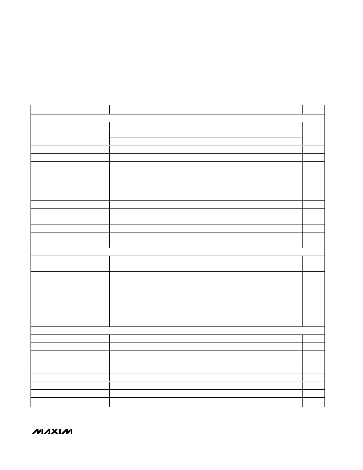
MAX1870A
Step-Up/Step-Down
Li+ Battery Charger
_______________________________________________________________________________________ 7
PARAMETER CONDITIONS
UNITS
SUPPLY AND LINEAR REGULATOR
DCIN Input Voltage Range 8 28 V
DCIN falling 4
DCIN Undervoltage Lockout
DCIN rising
V
DCIN Quiescent Current 8.0V < V
DCIN
< 28V 6 mA
BATT Input Voltage Range 0 19 V
BATT Input Bias Current
µA
LDO Output Voltage No load 5.3 5.5 V
LDO Undervoltage Lockout V
DCIN
= 8V, LDO rising
V
REFERENCE
REF Output Voltage I
REF
= 0µA
V
REF Load Regulation 0 < I
REF
< 500µA 10 mV
REF Undervoltage-Lockout Trip
Point
V
REF
falling 3.9 V
REFIN Input Range 2.5 3.6 V
REFIN UVLO Rising 2.2 V
REFIN Input Bias Current V
DCIN
= 18V 100 µA
SWITCHING REGULATOR
C ycl e- b y- C ycl e S tep - U p M axi m um
C ur r ent- Li m i t S ense V ol tag e
V
DCIN
= 12V, V
BATT
= 16.8V
130 170 mV
C ycl e- b y- C ycl e S tep - D ow n
M axi m um C ur r ent- Li m i t S ense
V ol tag e
V
DCIN
= 19V, V
BATT
= 16.8V 130 170 mV
Step-Down On-Time V
DCIN
= 18V, V
BATT
= 16.8V 2.2 2.6 µs
Minimum Step-Down Off-Time V
DCIN
= 18V, V
BATT
= 16.8V
µs
Step-Up Off-Time V
DCIN
= 12V, V
BATT
= 16.8V 1.6 2.0 µs
Minimum Step-Up On-Time V
DCIN
= 12V, V
BATT
= 16.8V
µs
MOSFET DRIVERS
VHP - VHN Output Voltage 8V < V
VHP
< 28V, no load 4.5 5.5 V
VHN Load Regulation 0 < I
VHN
< 10mA 150 mV
DHI On-Resistance High I
SOURCE
= 10mA 5 Ω
DHI On-Resistance Low I
SINK
= 10mA 3 Ω
VHP Input Bias Current
mA
BLKP Input Bias Current
µA
DLOV Supply Current DBST low 10 µA
DBST On-Resistance High I
SOURCE
= 10mA 5 Ω
DBST On-Resistance Low I
SINK
= 10mA 3 Ω
ELECTRICAL CHARACTERISTICS
(Circuit of Figure 2, V
DCIN
= V
CSSP
= V
CSSN
= V
CSSS
= V
VHP
= 18V, V
BATT
= V
CSIP
= V
CSIN
= V
BLKP
= 12V, V
REFIN
= 3.0V, V
ICTL
=
0.75 x V
REFIN
, VCTL = LDO, CELLS = FLOAT, GND = PGND = 0, V
DLOV
= 5.4V, TA= -40°C to +85°C.) (Note 1)
MIN TYP MAX
7.85
V
= 2V to 19V
BATT
4.00
500
5.25
4.060
4.132
0.15
0.50
0.15
0.40
V
= 18V
DCIN
V
ICTL
= V
REFIN
= 3.3V
2
400
Page 8
MAX1870A
Step-Up/Step-Down
Li+ Battery Charger
8 _______________________________________________________________________________________
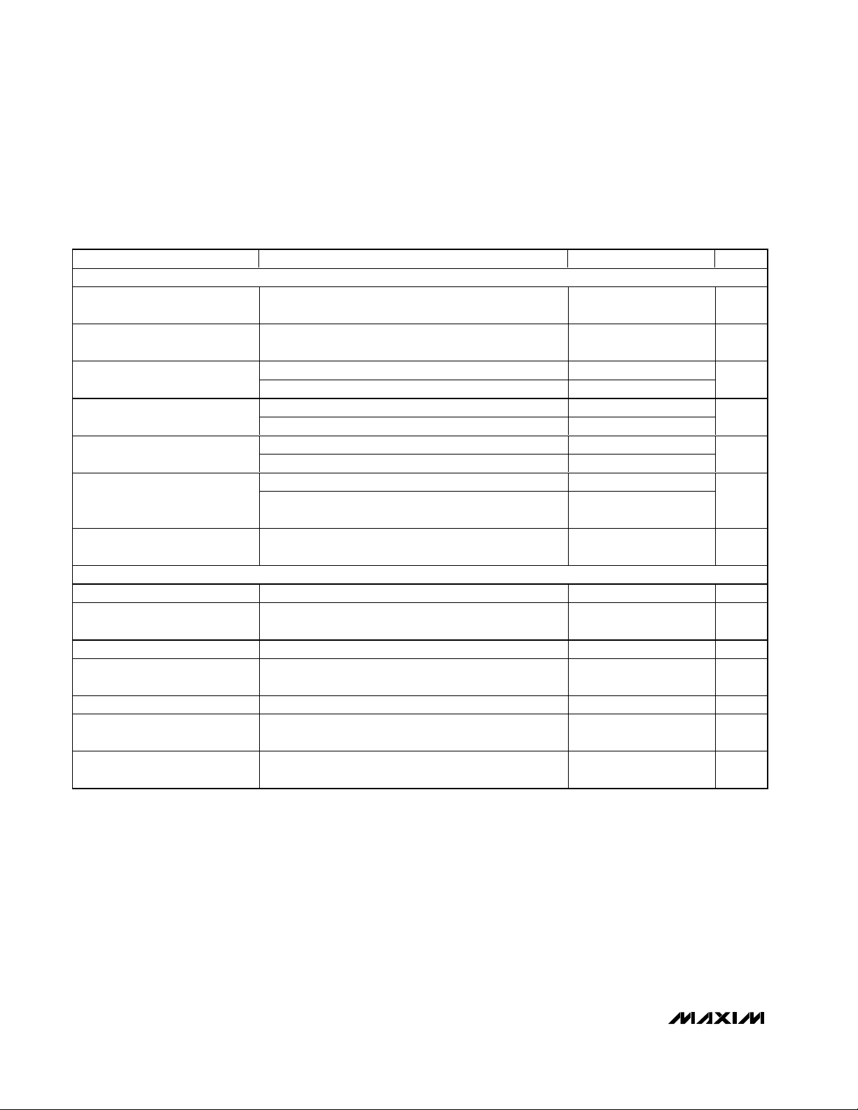
PARAMETER CONDITIONS
MIN
TYP
MAX
UNITS
ERROR AMPLIFIERS
GMV Amplifier Loop
Transconductance
V C TL = RE FIN , V
BAT T
= 16.8V
µA/mV
GMI Amplifier Loop
Transconductance
ICTL = REFIN, V
CSIP
- V
CSIN
= 72mV 1.8 3.0
µA/mV
V
CLS
= REF, V
CSSP
- V
CSSN
= 102mV, V
CSSP
= V
CSSS
1.2 2.2
GMS Amplifier Loop
Transconductance
V
CLS
= REF, V
CSSP
- V
CSSS
= 102mV, V
CSSP
= V
CSSN
1.2 2.2
µA/mV
VCTL = REFIN, V
BATT
= 15.8V 50
CCV Output Current
VCTL = REFIN, V
BATT
= 17.8V -50
µA
ICTL = REFIN, V
CSIP
- V
CSIN
= 0mV
CCI Output Current
ICTL = REFIN, V
CSIP
- V
CSIN
= 150mV
µA
CLS = REF, V
CSSP
= V
CSSN
, V
CSSP
= V
CSSS
CCS Output Current
CLS = REF, V
CSSP
- V
CSSN
= 200mV,
V
CSSP
- V
CSSS
= 200mV
µA
CCI/CCS/CCV Clamp Voltage
1.1V < V
CCV
< 3.5V, 1.1V < V
CCS
< 3.5V,
1.1V < V
CCI
< 3.5V
500 mV
LOGIC LEVELS
ASNS Output-Voltage Low V
IINP
= GND, I
SINK
= 1mA 0.4 V
ASNS Output-Voltage High V
IINP
= 4V, I
SOURCE
= 1mA
LDO -
0.5
V
ASNS Current Detect V
IINP
rising 1.1
1.2 V
SHDN Threshold SHDN falling, V
REFIN
= 2.8V to 3.6V 22 25
% of
REFIN
CELLS Input Low Voltage
V
CELLS Float Voltage 40 60
% of
REFIN
CELLS Input High Voltage
RE FIN -
V
ELECTRICAL CHARACTERISTICS
(Circuit of Figure 2, V
DCIN
= V
CSSP
= V
CSSN
= V
CSSS
= V
VHP
= 18V, V
BATT
= V
CSIP
= V
CSIN
= V
BLKP
= 12V, V
REFIN
= 3.0V, V
ICTL
=
0.75 x V
REFIN
, VCTL = LDO, CELLS = FLOAT, GND = PGND = 0, V
DLOV
= 5.4V, TA= -40°C to +85°C.) (Note 1)
Note 1: Specifications to -40°C are guaranteed by design, not production tested.
0.05
0.20
150
-150
100
-100
100
0.75V
1.15
0.75
Page 9
MAX1870A
Step-Up/Step-Down
Li+ Battery Charger
_______________________________________________________________________________________ 9
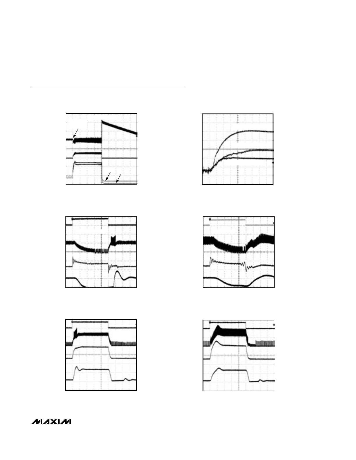
BATTERY INSERTION AND REMOVAL
MAX1870Atoc01
V
BATT
18V
16V
I
CHARGE
5A/div
0
CCI AND CCV
CCI
CCV
0
2V
4V
20V
2.00ms/div
BATTERY REMOVAL
BATTERY
INSERTION
CCV
CCI
BATTERY-REMOVAL RESPONSE
MAX1870Atoc02
V
BATT
21V
18V
20V
19V
16V
17V
10.0µs/div
RCV = 10kΩ, C
OUT
= 22µF
RCV = 10kΩ, C
OUT
= 44µF
RCV = 20kΩ, C
OUT
= 44µF
SYSTEM LOAD-TRANSIENT RESPONSE
MAX1870Atoc03
4A
2A
0A
INDUCTOR CURRENT
SYSTEM LOAD
INPUT CURRENT
BATTERY CURRENT
5A
0A
2A
0A
0A
5A
200µs
STEP-DOWN MODE
SYSTEM LOAD-TRANSIENT RESPONSE
MAX1870Atoc04
4A
2A
0A
INDUCTOR CURRENT
SYSTEM LOAD
INPUT CURRENT
BATTERY CURRENT
5A
0A
2A
0A
0A
5A
100µs
HYBRID MODE
CHARGE-CURRENT STEP RESPONSE
MAX1870Atoc05
2A
0A
1V
INDUCTOR CURRENT
BATTERY CURRENT
0V
CCI
0A
2A
0V
5V
V
ICTL
400µs
STEP-DOWN
MODE
CHARGE-CURRENT STEP RESPONSE
MAX1870Atoc06
2A
0A
1V
INDUCTOR CURRENT
BATTERY CURRENT
0V
CCI
0A
2A
0V
5V
V
ICTL
400µs
HYBRID MODE
Typical Operating Characteristics
(Circuit of Figure 1, V
DCIN
= 16V, CELLS = REFIN, V
CLS =VREF
, V
ICTL
= V
REFIN
= 3.3V, TA= +25°C, unless otherwise noted.)
Page 10
MAX1870A
Step-Up/Step-Down
Li+ Battery Charger
10 ______________________________________________________________________________________
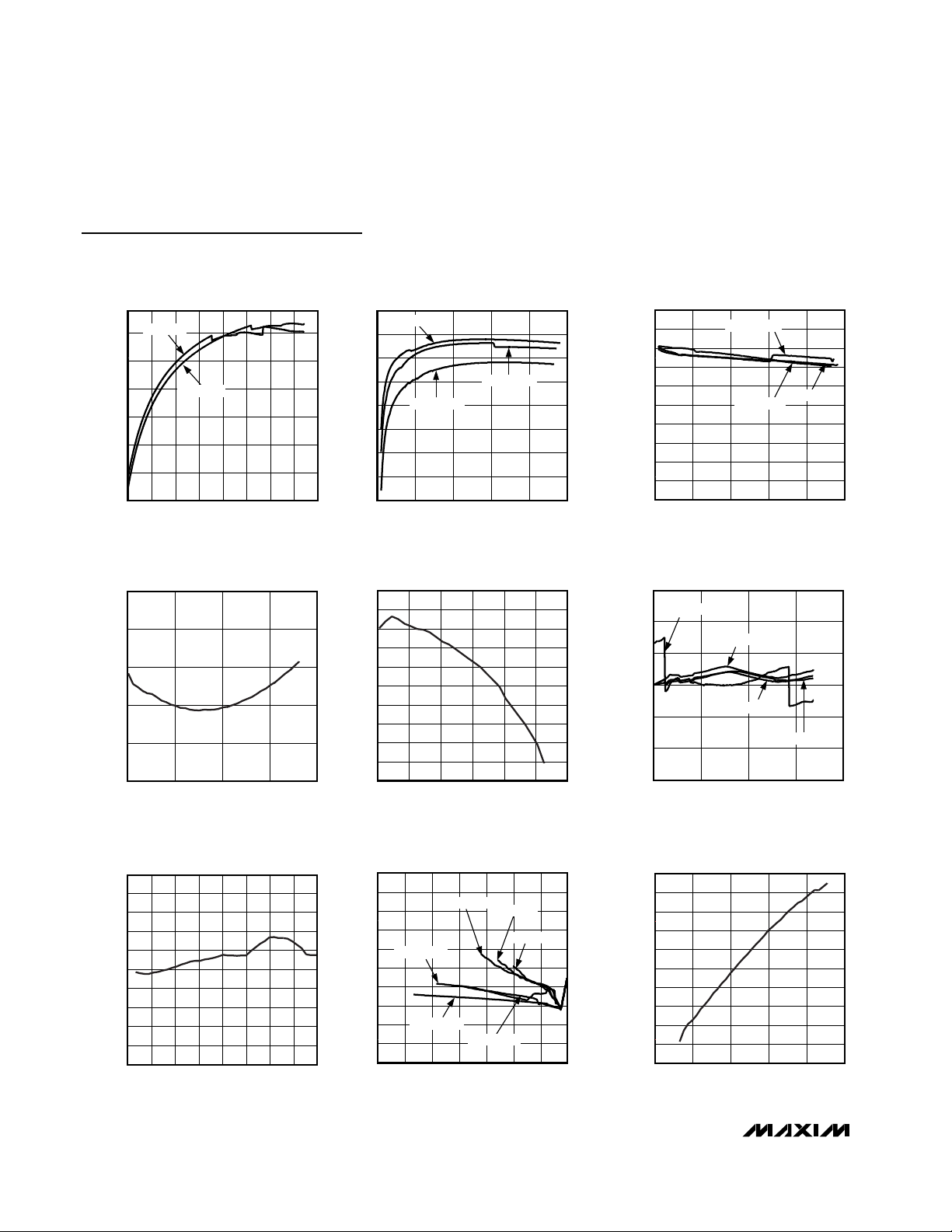
Typical Operating Characteristics (continued)
(Circuit of Figure 1, V
DCIN
= 16V, CELLS = REFIN, V
CLS =VREF
, V
ICTL
= V
REFIN
= 3.3V, TA= +25°C, unless otherwise noted.)
EFFICIENCY vs. BATTERY VOLTAGE
MAX1870A toc07
BATTERY VOLTAGE (V)
EFFICIENCY (%)
124 81614610
65
70
75
80
90
85
95
60
218
V
IN =
12V
V
IN =
16V
EFFICIENCY vs. CHARGE CURRENT
MAX1870A toc08
CHARGE CURRENT (A)
EFFICIENCY (%)
2.01.50.5 1.0
65
70
75
80
90
85
95
100
60
0 2.5
V
BATT =
16.8V
V
BATT =
8.4V
V
BATT =
12.6V
BATTERY VOLTAGE ERROR IN CV MODE
MAX1870A toc09
CHARGE CURRENT (A)
BATTERY VOLTAGE ERROR (%)
2.01.50.5 1.0
-0.4
-0.3
-0.2
-0.1
0.2
0
0.4
0.1
0.3
0.5
-0.5
0 2.5
V
BATT =
16.8V
V
BATT =
12.6V
V
BATT =
8.4V
BATTERY VOLTAGE ERROR vs. VCTL
MAX1870Atoc10
VCTL (V)
BATTERY VOLTAGE ERROR (%)
3.002.001.00
0.05
0.10
0.15
0.20
0.25
0
0 4.00
CHARGE-CURRENT ERROR vs. ICTL
MAX1870Atoc11
V
ICTL
(V)
CHARGE-CURRENT ERROR (mA)
2.502.001.501.000.50
-70
-60
-50
-40
-30
-20
-10
0
10
20
-80
0 3.00
CHARGE-CURRENT ERROR
vs. BATTERY VOLTAGE
MAX1870Atoc12
V
BATT
(V)
CHARGE-CURRENT ERROR (%)
15105
-10
-5
0
5
10
15
-15
020
I
CHG =
0.15A
I
CHG =
2.4A
I
CHG =
1.9A
I
CHG =
1.4A
IINP ERROR vs. SYSTEM LOAD
MAX1870Atoc13
SYSTEM LOAD (A)
IINP ERROR (mV)
3.02.00.5 1.5 3.52.51.0
-4
-2
0
2
4
-3
-1
1
3
5
-5
0 4.0
INPUT CURRENT-LIMIT ERROR
vs. SYSTEM CURRENT
MAX1870A toc14
SYSTEM CURRENT (A)
INPUT CURRENT-LIMIT ERROR (%)
3.02.50.5 1.51.0 2.0
-8
-6
-4
-2
4
0
8
2
6
10
-10
0 3.5
V
BATT =
16V
V
BATT =
14V
V
BATT =
10V
V
BATT =
8V
V
BATT =
6V
V
BATT =
12V
INPUT CURRENT-LIMIT ERROR
vs. CLS
MAX1870A toc15
V
CLS
(V)
INPUT CURRENT-LIMIT ERROR (mA)
4.002.001.00 3.00
-250
-200
-150
-100
50
-50
150
0
100
200
-300
0 5.00
Page 11

MAX1870A
Step-Up/Step-Down
Li+ Battery Charger
______________________________________________________________________________________ 11
Typical Operating Characteristics (continued)
(Circuit of Figure 1, V
DCIN
= 16V, CELLS = REFIN, V
CLS =VREF
, V
ICTL
= V
REFIN
= 3.3V, TA= +25°C, unless otherwise noted.)
REF LOAD REGULATION
MAX1870A toc16
LOAD CURRENT (µA)
V
REF
(V)
20001000500 1500
4.04
4.05
4.06
4.08
4.07
4.10
4.09
4.11
4.03
0 2500
REFERENCE ERROR vs. TEMPERATURE
MAX1870Atoc17
TEMPERATURE (°C)
REFERENCE ERROR (%)
806020 400-20
0.05
0.10
0.15
0.20
0.25
0.30
0.35
0.40
0.45
0
-40 100
LDO LOAD REGULATION
MAX1870A toc18
LOAD (mA)
V
LDO
(V)
403010 20
5.26
5.32
5.28
5.36
5.30
5.34
5.38
5.24
050
V
IN =
28V
V
IN =
16V
V
IN =
9V
LDO vs. TEMPERATURE
MAX1870A toc19
TEMPERATURE (°C)
LDO VOLTAGE ERROR (%)
8040-20 06020
-0.2
0.2
0.6
0
0.4
0.8
-0.4
-40 100
OUTPUT VOLTAGE RIPPLE
vs. BATTERY VOLTAGE
MAX1870Atoc20
V
BATT
(V)
RMS OUTPUT RIPPLE (mV)
15105
20
40
60
80
100
120
140
160
180
0
020
STEP-UP/STEP-DOWN
SWITCHING WAVEFORM
MAX1870Atoc21
0V
D4
10V
0V
CATHODE
D3 ANODE
INDUCTOR CURRENT
4A
V
BATT
(AC-COUPLED)
200mV/div
2A
10V
20V
2.00µs
VIN = 16V
V
BATT
= 16V
STEP-DOWN
SWITCHING WAVEFORM
MAX1870Atoc22
0V
D4
10V
0V
CATHODE
D3 ANODE
INDUCTOR CURRENT
4A
V
BATT
(AC-COUPLED)
10mV/div
2A
10V
20V
2.00µs
VIN = 16V
V
BATT
= 12V
Page 12

MAX1870A
Step-Up/Step-Down
Li+ Battery Charger
12 ______________________________________________________________________________________
Typical Operating Characteristics (continued)
(Circuit of Figure 1, V
DCIN
= 16V, CELLS = REFIN, V
CLS =VREF
, V
ICTL
= V
REFIN
= 3.3V, TA= +25°C, unless otherwise noted.)
Pin Description
PIN NAME FUNCTION
1 LDO
Device Power Supply. Output of the 5.4V linear regulator supplied from DCIN. Bypass LDO to GND with
a 1µF or greater ceramic capacitor.
2 REF 4.096V Voltage Reference. Bypass REF to GND with a 1µF or greater ceramic capacitor.
3 CLS
Source Current-Limit Input. Voltage input for setting the current limit of the input source. See the Setting
the Input Current Limit section.
4, 8 GND Analog Ground
5 CCV
Voltage Regulation Loop Compensation Point. Connect a 10kΩ resistor in series with a 0.01µF capacitor
to GND.
6 CCI Charge-Current Regulation Loop Compensation Point. Connect a 0.01µF capacitor to GND.
7 CCS Input-Current Regulation Loop Compensation Point. Connect a 0.01µF capacitor to GND.
9 REFIN Reference Input. ICTL and VCTL are ratiometric with respect to REFIN for increased accuracy.
10 ASNS
Adapter Sense Output. Logic output is high when input current is greater than 1.5A (using 30mΩ sense
resistors and a 10kΩ resistor from IINP to GND).
11 VCTL
Charge-Voltage Control Input. Drive VCTL from 0 to V
REFIN
to adjust the charge voltage from 4V to 4.4V
per cell. See the Setting the Charge Voltage section.
STEP-UP
SWITCHING WAVEFORM
VIN = 12V
= 16V
V
BATT
2.00µs
20V
10V
CATHODE
D4
MAX1870Atoc23
0V
10V
D3 ANODE
0V
4A
INDUCTOR CURRENT
2A
V
BATT
(AC-COUPLED)
50mV/div
STEP-UP/STEP-DOWN
LIGHT LOAD
VIN = 16V
= 16V
V
BATT
CHARGE CURRENT = 300mA
2.00µs
20V
10V
CATHODE
D4
MAX1870Atoc24
0V
10V
D3 ANODE
0V
4A
INDUCTOR CURRENT
2A
V
BATT
(AC-COUPLED)
50mV/div
Page 13

MAX1870A
Step-Up/Step-Down
Li+ Battery Charger
______________________________________________________________________________________ 13
Pin Description (continued)
PIN NAME FUNCTION
12 ICTL
Charge-Current Control Input. Drive ICTL from V
REFIN
/ 32 to V
REFIN
to adjust the charge current. See the
Setting the Charge Current section. Drive ICTL to GND to disable charging.
13 CELLS
Cell-Count Selection Input. Connect CELLS to GND for two Li+ cells. Float CELLS for three Li+ cells, or
connect CELLS to REFIN for four Li+ cells.
14 IINP
Input-Current Monitor Output. IINP is a replica of the input current sensed by the MAX1870. It represents
the sum of the current consumed by the charger and the current consumed by the system. IINP has a
transconductance of 2.8µA/mV.
15 SHDN
Shutdown Comparator Input. Pull SHDN low to stop charging. Optionally connect a thermistor to stop
charging when the battery temperature is too hot.
16 BATT Battery-Voltage Feedback Input
17 CSIN Charge Current-Sense Negative Input
18 CSIP
Charge Current-Sense Positive Input. Connect a current-sense resistor from CSIP to CSIN. Connect a
2.2µF capacitor from CSIP to GND.
19 BLKP Power Connection for Current-Sense Amplifier. Connect BLKP to BATT.
20, 21 I.C. Internally Connected. Do not connect this pin.
22 DBST Step-Up Power MOSFET (NMOS) Gate-Driver Output
23 PGND Power Ground
24 I.C. Internally Connected. Do not connect this pin.
25 DLOV Low-Side Driver Supply. Bypass DLOV with a 1µF capacitor to GND.
26 VHN
Power Connection for the High-Side MOSFET Driver. Bypass VHP to VHN with a 1µF or greater ceramic
capacitor.
27 DHI
High-Side Power MOSFET (PMOS) Driver Output. Connect to the gate of the high-side step-down
MOSFET.
28 VHP
Power Connection for the High-Side MOSFET Driver. Bypass VHP to VHN with a 1µF or greater ceramic
capacitor.
29 CSSN
Negative Terminal for Current-Sense Resistor for Charger Current. Connect a 2.2µF capacitor from CSSN
to GND.
30 CSSS Negative Terminal for Current-Sense Resistor for System Load Current
31 CSSP
Positive Terminal for Input Current-Sense Resistors. Connect a current-sense resistor from CSSP to
CSSN. Connect an equivalent sense resistor from CSSP to CSSS.
32 DCIN DC Supply Voltage Input. Bypass DCIN with a 1µF or greater ceramic capacitor to power ground.
Paddle Paddle. Connect to GND.
Page 14

MAX1870A
Step-Up/Step-Down
Li+ Battery Charger
14 ______________________________________________________________________________________
MAX1870A
234
VHP
VHN
CSSP
CSSN
DHI
DBST
CSIP
CSIN
BATT
DLOV
LDO
BLKP
CSSS
16
12
13
28
26
31
29
27
22
14
9
10
11
DCIN
REF
CLS
CCV
CCI
CCS
REFIN
ASNS
VCTL
ICTL
CELLS
IINP
PGND
32
18
17
25
1
15
7
6
5
3
2
AC
ADAPTER
VDD
HOST
DIGITAL INPUT
D/A OUTPUT
D/A OUTPUT
HI-IMPEDANCE
OUTPUT
LOGIC OUTPUT
A/D INPUT
GND
SYSTEM LOAD
+
-
R3
R4
R7
10kΩ
C6
0.01µF
C8
22µF
C9
44µF
C7
1µF
RS2
30mΩ
L1
10µH
C11
1µF
C12
1µF
M2
M1
19
N
P
RS1b
30mΩ
GND
30
RS1a
30mΩ
R6
33Ω
C5
1µF
C1
1µF
D1
D2
OPTIONAL REVERSE-
ADAPTER PROTECTION
2.2µF
2.2µF
D3
D4
R5
10kΩ
C2
0.01µF
C3
0.01µF
C4
0.01µF
SHDN
Figure 1. µC-Controlled Typical Application Circuit
Page 15

MAX1870A
Step-Up/Step-Down
Li+ Battery Charger
______________________________________________________________________________________ 15
23476
VHP
VHN
CSSP
CSSN
DHI
DBST
CSIP
CSIN
BATT
DLOV
LDO
BLKP
CSSS
16
28
26
31
29
27
22
DCIN
REF
CELLS
CLS
PGND
32
18
17
25
1
3
REFIN
9
VCTL
11
ICTL
12
ASNS
10
IINP
14
CCV
5
15
2
13
SYSTEM LOAD
C8
22µF
C9
44µF
C7
1µF
RS2
30mΩ
L1
10µH
C11
1µF
C12
1µF
M2
M1
19
N
P
RS1b
30mΩ
GNDCCSCCI
30
RS1a
30mΩ
R6
33Ω
C5
1µF
C1
1µF
2.2µF
2.2µF
D3
D4
R4
OPEN
R3
SHORT
R9
OPEN
R10
OPEN
R1
SHORT
R12
OPEN
LDO
R7
10kΩ
R5
10kΩ
C6
0.01µF
C3
0.01µF
C4
0.01µF
C2
0.01µF
SHDN
AC
ADAPTER
+
-
D1
D2
OPTIONAL
MAX1870A
OPTIONAL REVERSE-
ADAPTER PROTECTION
Figure 2. Stand-Alone Typical Application Circuit
Page 16

MAX1870A
Step-Up/Step-Down
Li+ Battery Charger
16 ______________________________________________________________________________________
Detailed Description
The MAX1870A includes all of the functions necessary
to charge Li+, NiMH, and NiCd batteries. A high-efficiency H-bridge topology DC-DC converter controls
charge voltage and current. A proprietary control
scheme offers improved efficiency and smaller inductor
size compared to conventional H-bridge controllers and
operates from input voltages above and below the battery voltage. The MAX1870A includes analog control
inputs to limit the AC adapter current, charge current,
and battery voltage. An analog output (IINP) delivers a
current proportional to the source current. The Typical
Application Circuit shown in Figure 1 uses a microcontroller (µC) to control the charge current or voltage,
while Figure 2 shows a typical application with the
charge voltage and current fixed to specific values for
the application. The voltage at ICTL and the value of
RS2 set the charge current. The voltage at VCTL and
the CELLS inputs set the battery regulation voltage for
the charger. The voltage at CLS and the value of R3 and
R4 set the source current limit.
The MAX1870A features a voltage-regulation loop
(CCV) and two current-regulation loops (CCI and CCS).
CCV is the compensation point for the battery voltage
regulation loop. CCI and CCS are the compensation
points for the battery charge current and supply current
loops, respectively. The MAX1870A regulates the
adapter current by reducing battery charge current
according to system load demands.
Setting the Charge Voltage
The MAX1870A provides high-accuracy regulation of
the charge voltage. Apply a voltage to VCTL to adjust
the battery-cell voltage limit. Set VCTL to a voltage
between 0 and V
REFIN
for a 10% adjustment of the battery cell voltage, or connect VCTL to LDO for a default
setting of 4.2V per cell. The limited adjustment range
reduces the sensitivity of the charge voltage to external
resistor tolerances. The overall accuracy of the charge
voltage is better than ±1% when using ±1% resistors to
divide down the reference to establish VCTL. The percell battery-termination voltage is a function of the battery chemistry and construction. Consult the battery
manufacturer to determine this voltage. Calculate battery voltage using the following equation:
where N
CELLS
is the cell count selected by CELLS.
VCTL is ratiometric with respect to REFIN to improve
accuracy when using resistive voltage-dividers.
Connect CELLS as shown in Table 1 to charge two,
three, or four cells. The cell count can either be hardwired or software controlled. The internal error amplifier
(GMV) maintains voltage regulation (see Figure 3 for
the Functional Diagram). Connect a 10kΩ resistor in
series with a 0.01µF capacitor from CCV to GND to
compensate the battery voltage loop. See the Voltage
Loop Compensation section for more information.
Setting the Charge Current
Set the maximum charge current using ICTL and the
current-sense resistor RS2 connected between CSIP
and CSIN. The current threshold is set by the ratio of
V
ICTL
/ V
REFIN
. Use the following equation to program
the battery charge current:
where V
CSIT
is the full-scale charge current-sense
threshold, 73mV (typ). The input range for ICTL is
V
REFIN
/ 32 to V
REFIN
. To shut down the MAX1870A,
force ICTL below V
REFIN
/ 100.
The internal error amplifier (GMI) maintains chargecurrent regulation (see Figure 3 for the Functional
Diagram). Connect a 0.01µF capacitor from CCI to GND
to compensate the charge-current loop. See the Charge-
Current Loop Compensation section for more information.
Setting the Input Current Limit
The total input current, from a wall adapter or other DC
source, is a function of the system supply current and
the battery charge current. The MAX1870A limits the wall
adapter current by reducing the charge current when the
input current exceeds the input current-limit set point. As
the system supply current rises, the available charge
current decreases linearly to zero in proportion to the
system current. After the charge current has fallen to
zero, the MAX1870A cannot further limit the wall adapter
current if the system current continues to increase.
I
V
R
x
V
V
CHG
CSIT
S
ICTL
REFIN
=
2
VNxVVx
V
V
BATT CELLS
VCTL
REFIN
=+
404.
Table 1. Cell-Count Programming Table
CELLS CELL COUNT
GND 2
Float 3
REFIN 4
Page 17

MAX1870A
Step-Up/Step-Down
Li+ Battery Charger
______________________________________________________________________________________ 17
MAX1870A
CSSN
CSSP
CSSS
CLS
CCS
ICTL
CCI
CSIP
CSIN
CCV
BATT
CELLS
VCTL
A = 18V/V
A = 18V/V
CSS
CURRENT-
SENSE
AMPLIFIERS
3.6V
(6.7A FOR 30mΩ)
IMAX1
INPUT-CURRENT BLOCK
GMS
IINP ASNS
Gm
0.81mV
(1.5A FOR 30mΩ)
50mV
REFIN
x
400mV
REFIN
x
GMI
A = 18V/V
CSI
22.5mV
(42mA ON
30mΩ)
(6.7A FOR 30mΩ)
3.6V
IZX
IMAX2
CHARGE-CURRENT BLOCK
+ 4.0V
4.2V
GMV
REF
CELL-
SELECT
LOGIC
BATTERY-VOLTAGE BLOCK
SHUTDOWN LOGIC
5.4V LINEAR
REGULATOR
4.096V
REFERENCE
DCIN
LDO
REF REFIN
1/55
CHG
RDY
ICTL
23% OF
REFIN
GND
PGND
DLOV
VHN
DHI
VHP
DBST
SHDN
LEVEL
SHIFT
STEP-UP/DOWN
CURRENT-MODE
STATE MACHINE
IMAX1
LVC IMIN
0.15V
LVC
LOWSIDE
DRIVER
HIGHSIDE
DRIVER
Figure 3. Functional Diagram
Page 18

MAX1870A
Step-Up/Step-Down
Li+ Battery Charger
18 ______________________________________________________________________________________
The input source current is the sum of the MAX1870A
quiescent current, the charger input current, and the
system load current. The MAX1870A’s 6mA maximum
quiescent current is minimal compared to the charge
and load currents. The actual wall adapter current is
determined as follows:
where η is the efficiency of the DC-DC converter (85%
to 95% typ), I
SYS_LOAD
is the system load current,
I
ADAPTER
is the adapter current, and I
CHARGE
is the
charge current.
By controlling the input current, the current require-
ments of the AC wall adapter are reduced, minimizing
system size and cost. Since charge current is reduced
to control input current, priority is given to system loads.
An internal amplifier compares the sum of (V
CSSP
-
V
CSSN
) and (V
CSSP
- V
CSSS
) to a scaled voltage set by
the CLS input. Drive V
CLS
directly or set with a resistive
voltage-divider between REF and GND. Connect CLS
to REF for the maximum input current limit of 105mV.
Sense resistors RS1a and RS1b set the maximumallowable wall adapter current. Use the same values for
RS1a, RS1b, and RS2. Calculate the maximum wall
adapter current as follows:
where V
CSST
is the full-scale source current-sense voltage threshold, and is 105mV (typ). The internal error
amplifier (GMS) maintains input-current regulation (see
Figure 3 for the Functional Diagram). Typically, connect
a 0.01µF capacitor from CCS to GND to compensate
the source current loop (GMS). See the Charge-Current
and Wall-Adapter-Current Loop Compensation for more
information.
Input Current Measurement
The MAX1870A includes an input-current monitor output, IINP. IINP is a scaled-down replica of the system
load current plus the input-referred charge current. The
output voltage range for IINP is 0 to 3.5V. The voltage
of IINP is proportional to the output current by the following equation:
V
IINP
= I
ADAPTER
x RS1_ x G
IINP
x R7
where I
ADAPTER
is the DC current supplied by the
AC adapter, G
IINP
is the transconductance of IINP
(2.8µA/mV typ), and R7 is the resistor connected
between IINP and ground.
In the Typical Application Circuit, the duty cycle and
AC load current affect the accuracy of V
IINP
(see the
Typical Operating Characteristics).
LDO Regulator
LDO provides a 5.4V supply derived from DCIN. The
low-side MOSFET driver is powered by DLOV, which
must be connected to LDO as shown in Figure 1. LDO
also supplies the 4.096V reference (REF) and most of
the internal control circuitry. Bypass LDO to GND with a
1µF or greater ceramic capacitor. Bypass DLOV to
PGND with a 1µF or greater ceramic capacitor.
AC Adapter Detection
The MAX1870A includes a logic output, ASNS, which
indicates AC adapter presence. When the system load
draws more than 1.5A (for 30mΩ sense resistors and
R7 is 10kΩ), the ASNS logic output pulls high.
Shutdown
When the AC adapter is removed, the MAX1870A shuts
down to a low-power state, and typically consumes less
than 1µA from the battery through the combined load of
the CSIP, CSIN, BLKP, and BATT inputs. The charger
enters this low-power state when DCIN falls below the
undervoltage-lockout (UVLO) threshold of 7.5V.
Alternatively, drive SHDN below 23.5% of V
REFIN
or
drive ICTL below V
REFIN
/ 100 to inhibit charge. This
suspends switching and pulls CCI, CCS, and CCV to
ground. The LDO, input current monitor, and control
logic all remain active in this state.
Step-Up/Step-Down
DC-DC Controller
The MAX1870A is a step-up/step-down DC-DC controller. The MAX1870A controls a low-side n-channel
MOSFET and a high-side p-channel MOSFET to a constant output voltage with input voltage variation above,
near, and below the output. The MAX1870A implements
a patented control scheme that delivers higher efficiency with smaller components and less output ripple when
compared with other step-up/step-down control algorithms. This occurs because the MAX1870A operates
with lower inductor currents, as shown in Figure 4.
The MAX1870A proprietary algorithm offers the following benefits:
• Inductor current requirements are minimized.
• Low inductor-saturation current requirements allow
the use of physically smaller inductors.
• Low inductor current improves efficiency by reducing
I2R losses in the MOSFETs, inductor, and sense
resistors.
I
V
V
x
V
RS
ADAPTER MAX
CLS
REF
CSST
_
_=1
II
IxV
Vx
ADAPTER SYS LOAD
CHARGE BATT
IN
=+
_
η
Page 19

MAX1870A
Step-Up/Step-Down
Li+ Battery Charger
______________________________________________________________________________________ 19
• Continuous output current for V
IN
> 1.4 x V
OUT
reduces output ripple.
The MAX1870A uses the state machine shown in Figure
5. The controller switches between the states A, B, and C,
depending on VINand V
BATT
. State D provides PFM
operation during light loads. Under moderate and heavy
loads the MAX1870A operates in PWM.
Step-Down Operation
(V
IN
> 1.4 x V
BATT
)
During medium and heavy loads when V
IN
> 1.4 x
V
BATT
, the MAX1870A alternates between state A and
state B, keeping MOSFET M2 off (Figure 5). Figure 6
shows the inductor current in step-down operation.
During this mode, the MAX1870A regulates the stepdown off-time. Initially, DHI switches M1 off (state A) and
the inductor current ramps down with a dI/dt of V
BATT
/ L
until a target current is reached (determined by the error
integrator). After the target current is reached, DHI
switches M1 on (state B), and the inductor current ramps
up with a dI/dt of (V
IN
- V
BATT
) / L. M1 remains on until a
step-down on-time timer expires. This on-time is calculated based on the input and output voltage to maintain
pseudo-fixed-frequency 400kHz operation. At the end of
state B, another step-down off-time (state A) is initiated
and the cycle repeats. The off-time is valley regulated
according to the error signal. The error signal is set by
the charge current or source current if either is at its limit,
or the battery voltage if both charge current and source
current are below their respective current limits.
During light loads, when the inductor current falls to
zero during state A, the controller switches to state D to
reduce power consumption and avoid shuttling current
in and out of the output.
Step-Up Operation (V
IN
< 0.9 x V
BATT
)
When V
IN
< 0.9 x V
BATT
, the MAX1870A alternates
between state B and state C, keeping MOSFET M1 on.
In this mode, the controller looks like a simple step-up
controller. Figure 7 shows the inductor current in step-
A) CONVENTIONAL
ALGORITHM
B) MAX1870A
ALGORITHM
2 x I
CHARGE
SHADED REGIONS REPRESENT
CHARGE DELIVERED
TIME
Figure 4. Inductor Current for VIN= V
BATT
Table 2. MAX1870A H-Bridge Controller Advantages
MAX1870A H-BRIDGE CONTROLLER TRADITIONAL H-BRIDGE CONTROLLER
• Only 1 MOSFET switched per cycle
• Continuous output current in step-down mode
•2 MOSFETs switched per cycle
• Always discontinuous output current
(requires higher inductor currents)
Page 20

MAX1870A
Step-Up/Step-Down
Li+ Battery Charger
20 ______________________________________________________________________________________
up operation. During this mode, the MAX1870A regulates the step-up on-time. Initially DBST switches M2 on
(state C) and the inductor current ramps up with a dI/dt
of V
IN
/ L. After the inductor current crosses the target
current (set by the error integrators), DBST switches M2
off (state B) and the inductor current ramps down with
a dI/dt of (V
BATT
- VIN) / L. M2 remains off until a stepup off-time timer expires. This off-time is calculated
based on the input and output voltage to maintain
400kHz pseudo-fixed-frequency operation. The step-up
on-time is regulated by the error signal, set according
to the charge current or source current if either is at its
limit, or the battery voltage if both charge current and
source current are below their respective current limits.
Step-Up/Step-Down Operation
(0.9 x V
BATT
< V
IN
< 1.4 x V
BATT
)
The MAX1870A features a step-up/step-down mode
that eliminates dropout. Figure 8 shows the inductor
current in step-up/step-down operation. When VINis
within 10% of V
BATT
, the MAX1870A alternates through
states A, B, and C, following the order A, B, C, B, A, B,
C, etc., with the majority of the time spent in state B.
Since more time is spent in state B, the inductor ripple
current is reduced, improving efficiency.
The time in state C is peak-current regulated, and the
remaining time is spent in state B (Figure 8A). During
this operating mode, the average inductor current is
approximately 20% higher than the load current.
The time in state A is valley current and the remaining
time is spent in state B (Figure 8B). During this mode,
the average inductor current is approximately 10%
higher than the load current.
Alternative algorithms require inductor currents twice
as high, resulting in four times larger I2R losses and
inductors typically four times larger in volume.
IMIN, IMAX, CCMP, and ZCMP
The MAX1870A state machine utilizes five comparators
to decide which state to be in and when to switch
states (Figure 3). The MAX1870A generates an error
V
IN
V
OUT
M1
D3
D4
M2
STEP-DOWN OFF
V
IN
V
OUT
M1
M2
STEP-DOWN ON
STATE BSTATE A STATE C
V
IN
V
OUT
M1
M2
STEP-DOWN PFM
IDLE STATE D
V
IN
V
OUT
M1
M2
+-
STEP-DOWN
PWM
STEP-UP
PWM
STEP-UP OFF STEP-UP ON
D4
D2
D4
D3
D3
D3
Figure 5. MAX1870A State Machine
Page 21

MAX1870A
Step-Up/Step-Down
Li+ Battery Charger
______________________________________________________________________________________ 21
STATE B
STATE A
PRECALCULATED STEP-DOWN ON-TIME
VALLEY REGULATED OFF-TIME
dl
dt
VIN - V
OUT
L
=
dl
dt
V
OUT
L
=
V
IN
> 1.4 x V
BATT
DUTY = VIN / V
OUT
Figure 6. MAX1870A Step-Down Inductor Current Waveform
signal based on the integrated error of the input current, charge current, and battery voltage. The error signal, determined by the lowest voltage clamp (LVC),
sets the threshold for current-mode regulation. The following comparators are used for regulation:
IMIN: The MAX1870A operates in discontinuous conduction if LVC is below 0.15V, and does not initiate
another step-down on-time. In discontinuous step-up
conduction, the peak current is set by IMIN. The peak
inductor current in discontinuous step-up mode is:
where V
IMIN
is the IMIN comparator threshold, 0.15V,
and A
CSI
is the charge current-sense amplifier gain,
18V/V.
CCMP: CCMP compares the current-mode control
I
V
AxRS
PK
IMIN
CSI
>
2
STATE B
STATE C
PRECALCULATED OFF-TIME
PEAK REGULATED ON-TIME
dl
dt
VIN - V
OUT
L
=
dl
dt
V
OUT
L
=
V
IN
> 0.9 x V
BATT
DUTY = 1 - VIN / V
OUT
Figure 7. Step-Up Inductor-Current Waveform
Page 22

MAX1870A
Step-Up/Step-Down
Li+ Battery Charger
22 ______________________________________________________________________________________
point, LVC, to the inductor current. In step-down mode,
the off-time (state A) is terminated when the inductor
current falls below the current threshold set by LVC. In
step-up mode, the on-time (state C) is terminated when
the inductor current rises above the current threshold
set by LVC.
IMAX: The IMAX comparators provide a cycle-by-cycle
inductor current limit. This circuit compares the inductor current (CSI in step-down mode or CSS in step-up
mode) to the internally fixed cycle-by-cycle current
limit. The current-sense voltage limit is 200mV. With
RS1_ = RS2 = 30mΩ, which corresponds to 6.7A. If the
inductor current-sense voltage is greater than V
IMAX
(200mV), a step-up on-time is terminated or a stepdown on-time is not permitted.
ZCMP: The ZCMP comparator detects when the inductor current crosses zero. If the ZCMP output goes high
during a step-down off-time, the MAX1870A switches to
the idle state (state D) to conserve power.
Switching Frequency
The MAX1870A includes input and output-voltage feedforward to maintain pseudo-fixed-frequency (400kHz)
operation. The time in state B is set according to the
input voltage, output voltage, and a time constant. In
step-up/step-down mode the switching frequency is
STATE C
STATE B
STATE A
STATE B
STATE A
STATE B
STATE C
STATE B
A)
B)
MINIMUM
STEP-DOWN
OFF-TIME
PRECALCULATED STEP-UP
OFF-TIME
PRECALCULATED STEP-DOWN
ON-TIME
PRECALCULATED STEP-DOWN
ON-TIME
MINIMUM
STEP-UP
ON-TIME
PEAK REGULATED
STEP-UP
ON-TIME
VALLEY REGULATED
STEP-DOWN
OFF-TIME
dl
dt
V
BATT
- V
IN
L
=
dl
dt
V
IN
L
=
dl
dt
V
BATT
L
=
Figure 8. MAX1870A Step-Up/Step-Down Inductor-Current Waveform
Page 23

MAX1870A
Step-Up/Step-Down
Li+ Battery Charger
______________________________________________________________________________________ 23
effectively cut in half to allow for both the step-up cycle
and the step-down cycle. The switching frequency is
typically between 350kHz and 405kHz for VINbetween
8V and 28V. See the Typical Operating Characteristics.
Compensation
Each of the three regulation loops (the battery voltage,
the charge current, and the input current limit) are compensated separately using the CCV, CCI, and CCS
pins, respectively. Compensate the voltage regulation
loop with a 10kΩ resistor in series with a 0.01µF capacitor from CCV to GND. Compensate the charge current
loop and source current loop with 0.01µF capacitors
from CCI to GND and from CCS to GND, respectively.
Voltage Loop Compensation
When regulating the charge voltage, the MAX1870A
behaves as a current-mode step-down or step-up
power supply. Since a current-mode controller regulates
its output current as a function of the error signal, the
duty-cycle modulator can be modeled as a GM stage
(Figure 9). Results are similar in step-down, step-up, or
step-up/down, with the exception of a load-dependent
right-half-plane zero that occurs in step-up mode.
The required compensation network is a pole-zero pair
formed with CCVand RCV. CCVis chosen to be large
enough that its impedance is relatively small compared
to RCVat frequencies near crossover. RCVsets the
gain of the error amplifier near crossover. RCVand
C
OUT
determine the crossover frequency and, therefore, the closed-loop response of the system and the
response time upon battery removal.
R
ESR
is the equivalent series resistance (ESR) of the
charger’s output capacitor (C
OUT
). RLis the equivalent
charger output load, R
L
= ∆V
BATT
/ ∆I
CHG
= R
BATT
.
The equivalent output impedance of the GMV amplifier,
R
OGMV
, is greater than 10MΩ. The voltage loop
transconductance (GMV = ∆I
CCV
/ ∆V
BATT
) scales
inversely with the number of cells. GMV = 0.1µA/mV for
four cells, 0.133µA/mV for three cells, and 0.2µA/mV for
two cells. The DC-DC converter’s transconductance
depends upon the charge current-sense resistor RS2:
where A
CSI
= 18, and RS2 = 30mΩ in the Typical
Application Circuits, so GM
PWM
= 1.85A/V.
Use the following equation to calculate the loop transfer
function (LTF):
The poles and zeros of the voltage-loop transfer function are listed from lowest frequency to highest frequency in Table 3.
Near crossover, C
CV
has much lower impedance than
R
OGMV
. Since CCVis in parallel with R
OGMV, CCV
dominates the parallel impedance near crossover.
Additionally, RCVhas a much higher impedance than
CCVand dominates the series combination of RCVand
CCV, so:
C
OUT
also has a much lower impedance than RLnear
crossover, so the parallel impedance is mostly capacitive and:
If R
ESR
is small enough, its associated output zero has
a negligible effect near crossover and the loop transfer
function can be simplified as follows:
R
sC x R sC
L
OUT L OUT
()11+
≅
RxsCxR
sC x R
R near crossover
OGMV CV CV
CV OGMV
CV
()
()
,
11+
+
≅
LTF GM x
RxsCR
sC x R
x
R
sC x R
xG x sC xR
PWM
OGMV CV CV
CV OGMV
L
OUT L
MV OUT ESR
=
+
+
+
+
()
()
()
()
1
1
1
1
GM
AxRS
PWM
CSI
=
1
2
GM
OUT
REF
GMV
R
L
R
ESR
C
OUT
R
O
R
CV
C
CV
BATT
CCV
Figure 9. CCV Simplified Loop Diagram
Page 24

MAX1870A
Step-Up/Step-Down
Li+ Battery Charger
24 ______________________________________________________________________________________
Setting the LTF = 1 to solve for the unity-gain frequency
yields:
For stability, choose a crossover frequency lower than
1/10th of the switching frequency. The crossover frequency must also be below the RHP zero, calculated at
maximum charge current, minimum input voltage, and
maximum battery voltage.
Choosing a crossover frequency of 13kHz and solving for
RCVusing the component values listed in Figure 1 yields:
MODE = VCC(4 cells) GMV = 0.1µA/mV
C
OUT
= 22µF GM
PWM
= 1.85A/V
V
BATT
= 16.8V f
CO_CV
= 13kHz
R
L
= 0.2Ω f
OSC
= 400kHz
To ensure that the compensation zero adequately cancels the output pole, select f
Z_CV
≤
f
P_OUT
.
CCV≥ (RL / RCV) x C
OUT
CCV≥ 440pF
Figure 10 shows the Bode Plot of the voltage-loop frequency response using the values calculated above.
Charge-Current and Wall-Adapter-Current
Loop Compensation
When the MAX1870A regulates the charge current or the
wall adapter current, the system stability does not
depend on the output capacitance. The simplified
schematic in Figure 11 describes the operation of the
MAX1870A when the charge-current loop (CCI) is in control. The simplified schematic in Figure 12 describes the
operation of the MAX1870A when the source-current
R
xC xf
GMV x GM
k
CV
OUT CO CV
PWM
==
210π
_
Ω
fGMxG
R
xC
CO CV PWM MV
CV
OUT
_
=
2π
LTF GM x
R
sC
G
PWM
CV
OUT
MV
=
Table 3. Constant Voltage Loop Poles and Zeros
NO.
CALCULATION DESCRIPTION
1
Lowest Frequency Pole created by CCV and GMV’s finite output
resistance. Since R
OGMV
is very large (R
OGMV
> 10MΩ), this is
a low-frequency pole.
2
Voltage-Loop Compensation Zero. If this zero is lower than the
output pole, f
P_OUT
, then the loop transfer function
approximates a single-pole response near the crossover
frequency. Choose C
CV
to place this zero at least 1 decade
below crossover to ensure adequate phase margin.
3
Output
Pole
Outp ut P ol e For m ed w i th the E ffecti ve Load Resi stance R
L
and the
Outp ut C ap aci tance C
OU T
. RL i nfl uences the D C g ai n b ut d oes not
affect the stab i l i ty of the system or the cr ossover fr eq uency.
4
Output
Zero
Output ESR Zero. This zero can keep the loop from crossing
unity gain if f
Z_OUT
is less than the desired crossover
frequency. Therefore, choose a capacitor with an ESR zero
greater than the crossover frequency.
5
S tep - U p M od e RH P Z er o. Thi s zer o occur s b ecause of the i ni ti al
op p osi ng r esp onse of a step - up conver ter . E ffor ts to i ncr ease the
i nd uctor cur r ent r esul t i n an i m m ed i ate d ecr ease i n cur r ent
d el i ver ed , al thoug h eventual l y r esul t i n an i ncr ease i n cur r ent
d el i ver ed . Thi s zer o i s d ep end ent on char g e cur r ent and m ay
cause the system to g o unstab l e at hi g h cur r ents w hen i n step - up
m od e. A r i g ht- hal f- p l ane zer o i s d etr i m ental to b oth p hase and
g ai n. To ensur e stab i l i ty und er m axi m um l oad i n step - up m od e,
the cr ossover fr eq uency m ust b e l ow er than hal f of f
R H P Z
.
NAME
CCV Pole
f
PCV
_
=
2π
1
xR C
OGMV CV
f
CCV Zero
RHP Zero
f
ZCV
_
f
P OUT
_
Z OUT
_
f
RHPZ
=
=
=
=
=
π
xLI V
2
xR C
2π
xR C
2π
xR C
2π
V
π
2
V
IN
OUT OUT
1
CV CV
1
L OUT
1
ESR OUT
IN
xLI
L
2
Page 25

MAX1870A
Step-Up/Step-Down
Li+ Battery Charger
______________________________________________________________________________________ 25
loop (CCS) is in control. Since the output capacitor’s
impedance has little effect on the response of the current
loop, only a single pole is required to compensate this
loop. A
CSI
and A
CSS
are the internal gains of the currentsense amplifiers. RS2 is the charge current-sense resistor. RS1a and RS1b are the adapter current-sense
resistors. R
OGMI
and R
OGMS
are the equivalent output
impedance of the GMI and GMS amplifiers, which are
greater than 10MΩ. GMI is the charge-current amplifier
transconductance (2.4µA/mV). GMS is the adapter-current amplifier transconductance (1.7µA/mV.) GM
PWM
is
the DC-DC converter transconductance (1.85A/V).
Use the following equation to calculate the loop transfer
function:
which describes a single-pole system. Since GM
PWM
=
the loop-transfer function simplifies to:
Use the following equations to calculate the crossover
frequency:
For stability, choose a crossover frequency lower than
1/10th of the switching frequency and lower than half of
the RHP zero.
CCI= 10 GMI / (2π x f
OSC
), CCS= 10 GMS / (2π x f
OSC
)
This zero is inversely proportional to charge current
and may cause the system to go unstable at high currents when in step-up mode. A right-half-plane zero is
detrimental to both phase and gain. To also ensure stability under maximum load in step-up mode, the CCI
crossover frequency must also be lower than f
RHPZ
.
The right-half-plane zero does not affect CCS.
Choosing a crossover frequency of 30kHz and using
the component values listed in Figure 1 yields CCIand
C
CS_
> 10nF. Values for C
CI
/ CCSgreater than ten
times the minimum value may slow down the current
loop response excessively. Figure 13 shows the Bode
Plot of the input-current frequency response using the
values calculated above.
MOSFET Drivers
DHI and DBST are optimized for driving moderatelysized power MOSFETs. Use low-inductance and lowresistance traces from driver outputs to MOSFET gates.
DHI typically sources 1.6A and sinks 0.8A to or from
the gate of the p-channel MOSFET. DHI swings from
VHP to VHN. VHN is a negative LDO that regulates with
respect to VHP to provide high-side gate drive.
Connect VHP to DCIN. Bypass VHN with a 1µF capacitor to VHP.
f
V
xLI
V
LI V
RHPZ WorstCase
IN MIN
L
IN MIN
OUTMAX OUTMAX
_
__
==
22
2
ππ
f
GMI
C
f
GMS
C
CO CI
CI
CO CS
CS
__
,==
22ππ
LTF GM
R
sR x C
OGM
OGM C
=+_
_
__
1
1
AxRS
CS_
_
LTF GM x A x RS x GM
R
sR x C
PWM CS
OGM
OGM C
=
+
__ _
_
__
1
CCV LOOP RESPONSE
MAGNITUDE (dB)
-135
-90
-45
0
80
60
40
20
-40
-20
0
1.E+00 1.E+011.E+02 1.E+03 1.E+041.E+05 1.E+061.E-01
FREQUENCY (Hz)
MAG
PHASE
Figure 10. CCV Loop Response
GM
PWM
REF
GMI
R
OGMI
C
CI
CCI
RS2
A
CSI
CSI
Figure 11. CCI Simplified Loop Diagram
Page 26

MAX1870A
Step-Up/Step-Down
Li+ Battery Charger
26 ______________________________________________________________________________________
LDO provides a 5.4V supply derived from DCIN and
delivers over 10mA. The n-channel MOSFET driver
DBST is powered by DLOV and can source 2.5A and
sink 5A. Since LDO provides power to the internal analog circuitry, use an RC filter from LDO to DLOV as
shown in Figure 1 to minimize noise at LDO. LDO also
supplies the 4.096V reference (REF) and most of the
internal control circuitry. Bypass LDO with a 1µF or
greater capacitor to GND.
Applications Information
Component Selection
Table 4 lists the recommended components and refers
to the circuit of Figure 1. The following sections describe
how to select these components.
MOSFETs
The MAX1870A requires one p-channel MOSFET and
one n-channel MOSFET. Component substitutions are
permissible as long as the on-resistance and gate
charge are equal or lower and the voltage, current, and
power-dissipation ratings are high enough. If using a
lower-power application, scale down the MOSFETs with
lower gate charge and the MOSFET’s on-resistance
can be scaled up. For example, in a system designed
to deliver half as much current, MOSFETs selected with
twice the on-resistance and half as much gate charge
ensure equal or better efficiency, and reduce size and
cost. If resistive losses dominate, it can be possible to
reduce the gate charge at the cost of on-resistance
and still achieve a similar efficiency.
Make sure that the linear regulators can drive the
selected MOSFETs. The average current required to
drive a given MOSFET is:
I
LDO
= Q
gM2
x f
switch
I
VHN
= Q
gM1
x f
switch
where f
switch
is 400kHz (typ).
GM
PWM
R
OGMS
C
CS
CCS
CLS
CSS
GMS
A
CSS
CSSP
CSSN/
CSSS
RS1_
Figure 12. CCS Simplified Loop Diagram
CCI LOOP RESPONSE
MAGNITUDE (dB)
-90
-45
0
80
60
40
20
-40
-20
0
100
1k100.1 100k
FREQUENCY (Hz)
CCS LOOP RESPONSE
MAGNITUDE (dB)
-90
-45
0
80
60
40
20
-40
-20
0
100
1k100.1 100k 10M
FREQUENCY (Hz)
PHASE
PHASE
MAG
MAG
Figure 13. CCI and CCS Loop Response
Page 27

MAX1870A
Step-Up/Step-Down
Li+ Battery Charger
______________________________________________________________________________________ 27
MOSFET Power Dissipation
Table 5 shows the resistive losses and switching losses
in each of the MOSFETs during either step-up or stepdown operation. Table 5 provides a first-order estimate,
but does not consider second-order effects such as
ripple current or nonlinear gate drive.
For typical applications where V
BATT
/ 2 < V
IN
< 2 x
V
BATT
, the resistive losses are primarily dissipated in M1
since M2 operates at a lower duty cycle. Switching losses are dissipated in M1 when in step-down mode and in
M2 when in step-up mode. Ratio the MOSFETs so that
resistive losses roughly equal switching losses when at
maximum load and typical input/output conditions. The
resistive loss equations are a good approximation in
hybrid mode (VINnear V
BATT
). Both M1 and M2 switch-
ing losses apply in hybrid mode.
Switching losses can become a heat problem when the
maximum AC adapter voltage is applied in step-down
operation or minimum AC adapter voltage is applied
with a maximum battery voltage. This behavior occurs
because of the squared term in the CV2f switching-loss
equation. Table 5 provides only an estimate and is not
a substitute for breadboard evaluation.
Inductor Selection
Select the inductor to minimize power dissipation in the
MOSFETs, inductor, and sense resistors. To optimize
resistive losses and RMS inductor current, set the LIR
(inductor current ripple) to 0.3. Because the maximum
resistive power loss occurs at the step-up boundary of
hybrid mode, select LIR for operating in this mode. Select
the inductance according to the following equation:
Larger inductance values can be used; however, they
contribute extra resistance that can reduce efficiency.
Smaller inductance values increase RMS currents and
can also reduce efficiency.
Saturation Current Rating
The inductor must have a saturation current rating high
enough so it does not saturate at full charge, maximum
output voltage, and minimum input voltage. In step-up
operation, the inductor carries a higher current than in
step-down operation with the same load. Calculate the
inductor saturation current rating by the following
equation:
Input-Capacitor Selection
The input capacitor must meet the ripple current
requirement (I
RMS
) imposed by the switching currents.
Nontantalum chemistries (ceramic, aluminum, or OS-
I
SAT
≥
V
OUT_MAXxICHG_MAX
V
IN _MIN
+
TxV
IN _ MIN
x1−
V
IN _MIN
V
OUT_MAX
2xL
L
xV xt
LIR I
IN
CHG
=
2
min
Table 4. Component List
DESIGNATION PART NUMBER SPECIFICATIONS
INDUCTORS
L1
Sumida CDRH104R-100
Sumida CDRH104R-7R0
Sumida CDRH104R-5R2
Sumida CDRH104R-3R8
10µH, 4.4A, 35mΩ power inductor
7µH, 4.8A, 27mΩ power inductor
5.2µH, 5.5A, 22mΩ power inductor
3.8µH, 6A, 13mΩ power inductor
P-CHANNEL MOSFETs
M1
Siliconix Si4435DY
Fairchild FDC602P
Fairchild FDS4435A
Fairchild FDW256P
P-FET 35mΩ, Q
G
= 17nC, V
DSMAX
= 30V, 8-pin SO
P-FET 35mΩ, Q
G
= 14nC, V
DSMAX
= 20V, 6-pin SuperSOT
P-FET 25mΩ, Q
G
= 21nC, V
DSMAX
= 30V, 8-pin SO
P-FET 20mΩ, Q
G
= 28nC, V
DSMAX
= 30V, 8-pin TSSOP
N/P-CHANNEL MOSFET PAIRS
M1/M2 Fairchild FDW2520C (8-pin TSSOP)
N-FET 18mΩ, Q
G
= 14nC, V
DSMAX
= 20V,
P-FET 35mΩ, Q
G
= 14nC, V
DSMAX
= 20V
N-CHANNEL MOSFETs
M2 IRF7811W N-FET, 9mΩ, QG = 18nC, V
DSMAX
= 30V, 8-pin SO
Page 28

MAX1870A
Step-Up/Step-Down
Li+ Battery Charger
28 ______________________________________________________________________________________
CON) are preferred due to their resilience to power-up
surge currents.
The input capacitors should be sized so that the temperature rise due to ripple current in continuous conduction
does not exceed approximately 10°C. Choose a capacitor with a ripple current rating higher than 0.5 x I
CHG
.
Output-Capacitor Selection
The output capacitor absorbs the inductor ripple current
in step-down mode, or a peak-to-peak ripple current
equal to the inductor current when in step-up or hybrid
mode. As such, both capacitance and ESR are important parameters in specifying the output capacitor. The
actual amplitude of the ripple is the combination of the
two. Ceramic devices are preferable because of their
resilience to surge currents. The worst-case output ripple
occurs during hybrid mode when the input voltage is at
its minimum. See the Typical Operating Characteristics.
Select a capacitor that can handle 0.5 x I
CHG
x V
BATT
/
VINwhile keeping the rise in capacitor temperature less
than 10°C. Also, select the output capacitor to tolerate
the surge current delivered from the battery when it is
initially plugged into the charger.
Battery-Removal Response
Upon battery removal, the MAX1870A continues to regulate a constant inductor current until the battery voltage, V
BATT
, exceeds the regulation threshold. The
MAX1870A’s response time depends on the bandwidth
of the CCV loop, f
CO
(see the Voltage Loop
Compensation section). For applications where battery
overshoot is critical, either increase C
OUT
or increase
f
CO
by increasing RCV. See Battery Insertion and
Removal in the Typical Operating Characteristics.
System Load Transient
The MAX1870A battery charger features a very fast
response time to system load transients. Since the
input current loop is configured as a single-pole system, the MAX1870A responds quickly to system load
transients (see the System Load-Transient Response
graph in the Typical Operating Characteristics). This
reduces the risk of tripping the overcurrent threshold of
the wall adapter and minimizes requirements for
adapter oversizing.
Table 5. MOSFET Resistive and Switching Losses
STEP-DOWN MODE STEP-UP MODE
DESIGNATION
DC LOSSES
M1
D4 0
M2 0
D3 I
CHG
x V
DIODE
I
CHG
x V
DIODE
SWITCHING LOSSES
M1 0
D4 0 0
M2 0
D3 0 0
Note: CLXis the total parasitic capacitance at the drain terminals of M1 and M2. I
GATE
is the peak gate-drive source/sink current of
M1 or M2.
V
V
xI xR
BATT
DCIN
CHG DS ON
2
()
V
V
xI xR
BATT
DCIN
CHG DS ON
2
()
1 −
V
V
xI V
BATT
DCIN
CHG Diode
12−
V
V
x
V
V
xI xR
DCIN
BATT
BATT
DCIN
CHG DS ON()
VxCxfI
I
DCIN MAX LX SW CHG
GATE
()
2
VxCxfI
IxV
BATT MAX LX SW CHG
GATE DCIN MAX
()
()
3
Page 29

MAX1870A
Step-Up/Step-Down
Li+ Battery Charger
______________________________________________________________________________________ 29
Layout And Bypassing
Bypass DCIN with a 1µF to ground (Figure 1). Optional
diodes D1 and D2 protect the MAX1870A when the DC
power-source input is reversed. A signal diode for D1 is
adequate because DCIN only powers the LDO and the
internal reference. Good PC board layout is required to
achieve specified noise, efficiency, and stable performance. The PC board layout artist must be given
explicit instructions—preferably, a pencil sketch showing the placement of the power-switching components
and high-current routing. Refer to the PC board layout
in the MAX1870A evaluation kit for examples. A ground
plane is essential for optimum performance. In most
applications, the circuit is located on a multilayer
board, and full use of the four or more copper layers is
recommended. Use the top layer for high-current connections (PGND, DHI, VHP, VHN, BLKP, and DLOV),
the bottom layer for quiet connections (CSSP, CSSN,
CSSS, CSIP, CSIN, REF, CCV, CCI, CCS, DCIN, LDO
and GND), and the inner layers for an uninterrupted
ground plane. Use the following step-by-step guide:
1) Place the high-power connections first, with their
grounds adjacent:
• Minimize the current-sense resistor trace lengths,
and ensure accurate current sensing with Kelvin
connections. Use independent branches for CSSP,
CSSS, CSSN, CSIP, and CSIN.
• Minimize ground trace lengths in the high-current
paths.
• Minimize other trace lengths in the high-current paths.
• Use >5mm wide traces for high-current paths.
Ideally, surface-mount power components are flush
against one another with their ground terminals almost
touching. These high-current grounds are then connected to each other with a wide, filled zone of top-layer copper, so they do not go through vias. Other high-current
paths should also be minimized, but focus primarily on
short ground and current-sense connections to eliminate
about 90% of all PC board layout problems.
2) Place the IC and signal components. Keep the main
switching nodes (inductor connectons) away from
sensitive analog components (current-sense traces
and REF capacitor). Important: the IC must be no
further than 10mm from the current-sense resistors. Keep the gate-drive traces (DHI and DBST)
shorter than 20mm, and route them away from the
current-sense lines and REF. Place ceramic bypass
capacitors close to the IC. The bulk capacitors can
be placed further away. Bypass CSSP, CSSN, CSIN,
and CSIP to analog GND to reduce switching noise
and maintain input-current and charger-current accuracy. Place the current-sense input filter capacitors
under the part, connected directly to GND.
3) Use a single-point star ground placed directly
below the part. Connect the input ground trace,
power ground (subground plane), and normal
ground to this node.
Figure 14 shows a partial layout of the power path and
components. Refer to the EV kit data sheet for more
information.
Page 30

MAX1870A
Step-Up/Step-Down
Li+ Battery Charger
30 ______________________________________________________________________________________
32
31
30
29
28
27
26
9
10
11
12
13
14
15
18
19
20
21
22
23
24
7
6
5
4
3
2
1
MAX1870A
THIN QFN
TOP VIEW
REF
LDO
CLS
GND
CCV
CCI
CCS
8
GND
DCIN
CSSP
CSSS
CSSN
VHP
DHI
VHN
25
DLOV
I.C.
PGND
DBST
I.C.
I.C.
BLKP
CSIP
17
CSIN
SHDN
IINP
16
BATT
CELLS
ICTL
VCTL
ASNS
REFIN
Pin Configuration
NP
M1
M2
D3 D4
RS1a
RS1b
C8
C9
RS2
IN
BATT
PGND
LOAD
L1
Figure 14. Recommended Layout for the MAX1870A
Chip Information
TRANSISTOR COUNT: 6484
PROCESS: BiCMOS
Page 31

MAX1870A
Step-Up/Step-Down
Li+ Battery Charger
______________________________________________________________________________________ 31
Package Information
(The package drawing(s) in this data sheet may not reflect the most current specifications. For the latest package outline information,
go to www.maxim-ic.com/packages
.)
QFN THIN.EPS
D2
(ND-1) X e
e
D
C
PIN # 1
I.D.
(NE-1) X e
E/2
E
0.08 C
0.10 C
A
A1 A3
DETAIL A
0.15
C B
0.15 C A
E2/2
E2
0.10 M C A B
PIN # 1 I.D.
b
0.35x45∞
L
D/2
D2/2
L
C
L
C
e e
L
CC
L
k
k
LL
E
1
2
21-0140
PACKAGE OUTLINE
16, 20, 28, 32, 40L, THIN QFN, 5x5x0.8mm
DETAIL B
L
L1
e
Page 32

Package Information (continued)
(The package drawing(s) in this data sheet may not reflect the most current specifications. For the latest package outline information,
go to www.maxim-ic.com/packages
.)
COMMON DIMENSIONS
3.353.15
T2855-1 3.25 3.353.15 3.25
MAX.
3.20
EXPOSED PAD VARIATIONS
3.00T2055-2 3.10
D2
NOM.MIN.
3.203.00 3.10
MIN.E2NOM. MAX.
NE
ND
PKG.
CODES
1. DIMENSIONING & TOLERANCING CONFORM TO ASME Y14.5M-1994.
2. ALL DIMENSIONS ARE IN MILLIMETERS. ANGLES ARE IN DEGREES.
3. N IS THE TOTAL NUMBER OF TERMINALS.
4. THE TERMINAL #1 IDENTIFIER AND TERMINAL NUMBERING CONVENTION SHALL CONFORM TO JESD 95-1
SPP-012. DETAILS OF TERMINAL #1 IDENTIFIER ARE OPTIONAL, BUT MUST BE LOCATED WITHIN THE
ZONE INDICATED. THE TERMINAL #1 IDENTIFIER MAY BE EITHER A MOLD OR MARKED FEATURE.
5. DIMENSION b APPLIES TO METALLIZED TERMINAL AND IS MEASURED BETWEEN 0.25 mm AND 0.30 mm
FROM TERMINAL TIP.
6. ND AND NE REFER TO THE NUMBER OF TERMINALS ON EACH D AND E SIDE RESPECTIVELY.
7. DEPOPULATION IS POSSIBLE IN A SYMMETRICAL FASHION.
8. COPLANARITY APPLIES TO THE EXPOSED HEAT SINK SLUG AS WELL AS THE TERMINALS.
9. DRAWING CONFORMS TO JEDEC MO220, EXCEPT EXPOSED PAD DIMENSION FOR T2855-1,
T2855-3 AND T2855-6.
NOTES:
SYMBOL
PKG.
N
L1
e
E
D
b
A3
A
A1
k
10. WARPAGE SHALL NOT EXCEED 0.10 mm.
JEDEC
T1655-1
3.203.00 3.10 3.00 3.10 3.20
0.70 0.800.75
4.90
4.90
0.25
0.250--
4
WHHB
4
16
0.350.30
5.10
5.105.00
0.80 BSC.
5.00
0.05
0.20 REF.
0.02
MIN. MAX.NOM.
16L 5x5
3.10
T3255-2
3.00
3.20
3.00 3.10 3.20
2.70T2855-2 2.60 2.602.80 2.70 2.80
E
2
2
21-0140
PACKAGE OUTLINE
16, 20, 28, 32, 40L, THIN QFN, 5x5x0.8mm
L
0.30 0.500.40
---
---
WHHC
20
5
5
5.00
5.00
0.30
0.55
0.65 BSC.
0.45
0.25
4.90
4.90
0.25
0.65
--
5.10
5.10
0.35
20L 5x5
0.20 REF.
0.75
0.02
NOM.
0
0.70
MIN.
0.05
0.80
MAX.
---
WHHD-1
28
7
7
5.00
5.00
0.25
0.55
0.50 BSC.
0.45
0.25
4.90
4.90
0.20
0.65
--
5.10
5.10
0.30
28L 5x5
0.20 REF.
0.75
0.02
NOM.
0
0.70
MIN.
0.05
0.80
MAX.
---
WHHD-2
32
8
8
5.00
5.00
0.40
0.50 BSC.
0.30
0.25
4.90
4.90
0.50
--
5.10
5.10
32L 5x5
0.20 REF.
0.75
0.02
NOM.
0
0.70
MIN.
0.05
0.80
MAX.
-
40
10
10
5.00
5.00
0.20
0.50
0.40 BSC.
0.40
0.25
4.90
4.90
0.15
0.60
5.10
5.10
0.25
40L 5x5
0.20 REF.
0.75
NOM.
0
0.70
MIN.
0.05
0.80
MAX.
0.20 0.25 0.30
-
0.35 0.45
0.30 0.40 0.50
DOWN
BONDS
ALLOWED
NO
YES3.103.00 3.203.103.00 3.20T2055-3
3.103.00 3.203.103.00 3.20T2055-4
T2855-3 3.15 3.25 3.35 3.15 3.25 3.35
T2855-6 3.15 3.25 3.35 3.15 3.25 3.35
T2855-4 2.60 2.70 2.80 2.60 2.70 2.80
T2855-5 2.60 2.70 2.80 2.60 2.70 2.80
T2855-7 2.60 2.70
2.80
2.60 2.70 2.80
3.20
3.00 3.10T3255-3 3.203.00 3.10
3.203.00 3.10T3255-4 3.203.00 3.10
3.403.20 3.30T4055-1 3.20 3.30 3.40
NO
NO
NO
NO
NO
NO
NO
NO
YES
YES
YES
YES
YES
3.203.00T1655-2 3.10 3.00 3.10 3.20 YES
MAX1870A
Step-Up/Step-Down
Li+ Battery Charger
Maxim cannot assume responsibility for use of any circuitry other than circuitry entirely embodied in a Maxim product. No circuit patent licenses are
implied. Maxim reserves the right to change the circuitry and specifications without notice at any time.
32 ____________________Maxim Integrated Products, 120 San Gabriel Drive, Sunnyvale, CA 94086 408-737-7600
© 2004 Maxim Integrated Products Printed USA is a registered trademark of Maxim Integrated Products.
 Loading...