

Page 1
General Description
The MAX1716/MAX1854/MAX1855 step-down controllers are intended for core CPU DC-DC converters in
notebook computers. They feature a dynamically
adjustable output (5-bit DAC), ultra-fast transient
response, high DC accuracy, and high efficiency needed for leading-edge CPU core power supplies. Maxim's
proprietary Quick-PWM™ quick-response, constant-ontime PWM control scheme handles wide input/output
voltage ratios with ease and provides 100ns “instant-on”
response to load transients while maintaining a relatively constant switching frequency.
The MAX1716/MAX1854/MAX1855 are designed
specifically for CPU core applications requiring a voltage-positioned supply. The voltage-positioning input
(VPS), combined with a high DC accuracy control loop,
is used to implement a power supply that modifies its
output set point in response to the load current. This
arrangement decreases full-load power dissipation and
reduces the required number of output capacitors.
The 28V input range of the MAX1716/MAX1854/MAX1855
enables single-stage buck conversion from high-voltage batteries for the maximum possible efficiency.
Alternatively, the devices’ high-frequency capability
combined with two-stage conversion (stepping down
the +5V system supply instead of the battery) allows
the smallest possible physical size. The output voltage
can be dynamically adjusted through the 5-bit digitalto-analog converter (DAC) inputs.
The MAX1716/MAX1854/MAX1855 are available in a
24-pin QSOP package. For applications requiring
SpeedStep™ power control (see the MAX1717).
________________________Applications
Notebook Computers
Docking Stations
CPU Core Supply
Single-Stage (BATT to V
CORE
) Converters
Two-Stage (+5V to V
CORE
) Converters
Features
♦ High-Efficiency Voltage Positioning
♦ Quick-PWM Architecture
♦ ±1% V
OUT
Line-Regulation Accuracy
♦ Adjustable Output Range (5-Bit DAC)
MAX1716: 0.925V to 1.6V
MAX1854: 0.925V to 2.0V
MAX1855: 0.600V to 1.75V
♦ 2V to 28V Input Range
♦ 200/300/400/550kHz Switching Frequency
♦ Output Undervoltage Protection
♦ Overvoltage Protection (MAX1716/MAX1855)
♦ Drive Large Synchronous-Rectifier MOSFETs
♦ 1.7ms Digital Soft-Start
♦ 700µA I
CC
Supply Current
♦ 1µA Shutdown Supply Current
♦ 2V ±1% Reference Output
♦ V
GATE
Transition-Complete Indicator
♦ Small 24-Pin QSOP Package
MAX1716/MAX1854/MAX1855
High-Speed, Adjustable, Synchronous Step-Down
Controllers with Integrated Voltage Positioning
________________________________________________________________ Maxim Integrated Products 1
19-1758; Rev 0; 8/00
For free samples and the latest literature, visit www.maxim-ic.com or phone 1-800-998-8800.
For small orders, phone 1-800-835-8769.
Pin Configuration appears at end of data sheet.
Quick-PWM is a trademark of Maxim Integrated Products.
SpeedStep is a trademark of Intel Corp.
Ordering Information
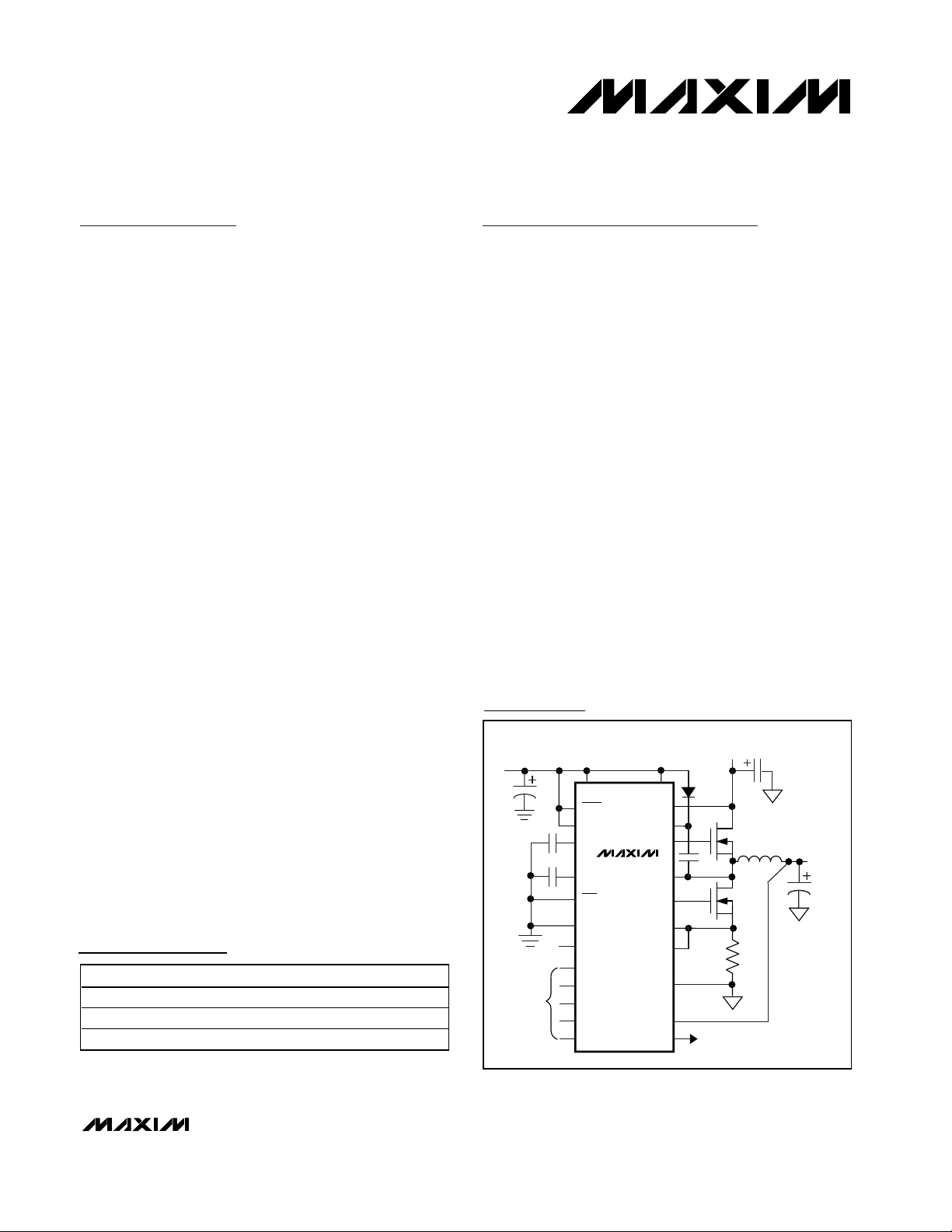
Typical Operating Circuit
PART TEMP. RANGE PIN-PACKAGE
MAX1716EEG -40°C to +85°C 24 QSOP
MAX1854EEG -40°C to +85°C 24 QSOP
MAX1855EEG -40°C to +85°C 24 QSOP
+5V INPUT
DAC
INPUTS
V
CC
SHDN
ILIM
REF
CC
SKIP
GND
TON
D0
D1
D2
D3
D4
MAX1716
MAX1854
MAX1855
V
BST
VPS
PGND
VGATE
DD
V+
DH
LX
DL
CS
FB
BATTERY
2V TO 28V
OUTPUT
Page 2

MAX1716/MAX1854/MAX1855
High-Speed, Adjustable, Synchronous Step-Down
Controllers with Integrated Voltage Positioning
2 _______________________________________________________________________________________
ABSOLUTE MAXIMUM RATINGS
ELECTRICAL CHARACTERISTICS
(Circuit of Figure 1, V+ = +15V, VCC= VDD= 5V, SKIP = VCC, VPS = PGND, TA= 0°C to +85°C, unless otherwise noted. Typical
values are at T
A
= +25°C.)
Stresses beyond those listed under “Absolute Maximum Ratings” may cause permanent damage to the device. These are stress ratings only, and functional
operation of the device at these or any other conditions beyond those indicated in the operational sections of the specifications is not implied. Exposure to
absolute maximum rating conditions for extended periods may affect device reliability.
Note 1: SKIP may be forced below -0.3V, temporarily exceeding the absolute maximum rating, for the purpose of debugging proto-
type breadboards, using the no-fault test mode. Limit the current drawn to -2mA (max).
V+ to GND ..............................................................-0.3V to +30V
V
CC
, VDDto GND .....................................................-0.3V to +6V
PGND to GND.....................................................................±0.3V
SHDN, VGATE to GND .............................................-0.3V to +6V
ILIM, FB, CC, REF, D0–D4, VPS,
TON to GND ...........................................-0.3V to (V
CC
+ 0.3V)
SKIP to GND (Note 1).................................-0.3V to (V
CC
+ 0.3V)
DL to PGND................................................-0.3V to (V
DD
+ 0.3V)
BST to GND ............................................................-0.3V to +36V
DH to LX....................................................-0.3V to (V
BST
+ 0.3V)
LX to BST..................................................................-6V to +0.3V
CS to GND.................................................................-2V to +30V
REF Short Circuit to GND ...........................................Continuous
Continuous Power Dissipation (T
A
= +70°C)
24-Pin QSOP (derate 9.5mW/°C above +70°C)...........762mW
Operating Temperature Range ...........................-40°C to +85°C
Junction Temperature......................................................+150°C
Storage Temperature Range .............................-65°C to +150°C
Lead Temperature (soldering, 10s) .................................+300°C
PWM CONTROLLER
Input Voltage Range
DC Output Voltage Accuracy
(Notes 2, 3)
FB Input Bias Current I
VPS Input Bias Current I
VPS Gain A
CS Input Bias Current I
ILIM Input Leakage Current I
Soft-Start Ramp Time 0 to full ILIM 1.7 ms
On-Time (Note 4) t
Minimum Off-Time (Note 4) t
PARAMETER SYMBOL CONDITIONS MIN TYP MAX UNITS
Battery voltage, V+ 2 28
V
, V
CC
DD
V+ = 4.5V to 28V,
VPS = PGND
FB
VPS
VPS
CS
ILIM
ON
OFF( M IN)
FB = 0.6V to 2.0V -0.2 0.2 µA
V
= ±40mV -1 1 µA
VPS
V
= 0 or -40mV, gain from VPS to FB 0.153 0.175 0.197 %/mV
VPS
0 to 28V -1 1 µA
V
= 0 or 5.0V 0.01 100 nA
ILIM
V+ = 11.0V,
V
= 1.5V
FB
DAC codes from
1.35V to 2.0V
DAC codes from
0.925V to 1.3V
DAC codes from
0.6V to 0.9V
TON = GND 205 255 300
TON = REF 280 327 375
TON = open 425 470 520
TON = V
CC
4.5 5.5
-1 1
-1.2 1.2
-1.5 1.5
615 678 740
400 500 ns
V
%
ns
Page 3

MAX1716/MAX1854/MAX1855
High-Speed, Adjustable, Synchronous Step-Down
Controllers with Integrated Voltage Positioning
_______________________________________________________________________________________ 3
ELECTRICAL CHARACTERISTICS (continued)
(Circuit of Figure 1, V+ = +15V, VCC= VDD= 5V, SKIP = VCC, VPS = PGND, TA= 0°C to +85°C, unless otherwise noted. Typical
values are at T
A
= +25°C.)
BIAS AND REFERENCE
Quiescent Supply Current (VCC)I
Quiescent Supply Current (VDD)I
Quiescent Supply Current (V+) I+ 25 40 µA
Shutdown Supply Current (VCC) SHDN = GND <1 5 µA
Shutdown Supply Current (VDD) SHDN = GND <1 5 µA
Shutdown Supply Current (V+) SHDN = GND, VCC = VDD = 0 or 5V <1 5 µA
Reference Voltage V
Reference Load Regulation I
REF Sink Current I
REF Fault Lockout Voltage Falling edge 1.6 V
FAULT PROTECTION
Output Overvoltage Fault
Threshold (Note 5)
Output Overvoltage Fault
Propagation Delay (Note 5)
Output Undervoltage Fault
Threshold (Foldback)
Output Undervoltage Fault
Propagation Delay
Output Undervoltage Fault
Blanking Time (Foldback)
Current-Limit Threshold
(Positive, Default)
Current-Limit Threshold
(Positive, Adjustable)
Negative Current-Limit
Threshold
Zero-Crossing Current-Limit
Threshold
Thermal Shutdown Threshold Hysteresis = 10°C 150 °C
VCC Undervoltage Lockout
Threshold
PARAMETER SYMBOL CONDITIONS MIN TYP MAX UNITS
V
V
CC
DD
REF
REF
ITH
ITH
Measured at VCC, FB forced above the
regulation point
Measured at VDD, FB forced above the
regulation point
VCC = 4.5V to 5.5V, no external REF load 1.98 2 2.02 V
= 0 to 50µA 0.01 V
REF
REF in regulation 10 µA
Measured at FB
FB forced to 2% above trip threshold
(MAX1716/MAX1855 only)
FB forced to 2% below trip threshold 10 µs
From SHDN signal going high 10 30 ms
V
- VCS, ILIM = V
PGND
V
- V
PGND
V
PGND
V
PGND
Rising edge, hysteresis = 20mV, switching
disabled below this level
- V
- V
CS
CS
CS
MAX1716 1.8 1.9 2.0
MAX1855 1.97 2.0 2.03
35 40 45 %
CC
V
= 0.5V 40 50 60
ILIM
V
= 2V (REF) 170 200 230
ILIM
110 120 130 mV
4.0 4.45 V
700 950 µA
<1 5 µA
V
1.5 µs
mV
-1.2 ×
V
ITH
3mV
mV
Page 4

MAX1716/MAX1854/MAX1855
High-Speed, Adjustable, Synchronous Step-Down
Controllers with Integrated Voltage Positioning
4 _______________________________________________________________________________________
ELECTRICAL CHARACTERISTICS (continued)
(Circuit of Figure 1, V+ = +15V, VCC= VDD= 5V, SKIP = VCC, VPS = PGND, TA= 0°C to +85°C, unless otherwise noted. Typical
values are at T
A
= +25°C.)
)
VGATE Lower Trip Threshold
VGATE Upper Trip Threshold
VGATE Propagation Delay
VGATE Output Low Voltage I
VGATE Leakage Current High state, forced to 5.5V 1 µA
GATE DRIVERS
DH Gate Driver On-Resistance R
DL Gate Driver On-Resistance R
DH Gate Driver Source/Sink
Current
DL Gate Drive Sink Current I
DL Gate Driver Source Current I
Dead-Time
LOGIC AND I/O
Logic Input High Voltage V
Logic Input Low Voltage V
TON Input Levels
Logic Input Current
D0−D4 Pullup Current D0−D4 = GND 3 5 10 µA
SKIP No-Fault Mode Current
PARAMETER SYMBOL CONDITIONS MIN TYP MAX UNITS
Measured at FB with respect to unloaded
output voltage, falling edge
Measured at FB with respect to unloaded
output voltage, rising edge
Falling edge, FB forced 2% below or above
VGATE trip threshold
SINK
ON ( D H ) VBST
ON(DL
I
DH
DL
DL
High state (pullup) 1.5 5
Low state (pulldown) 0.5 1.7
DH forced to 2.5V, V
DL forced to 5V 3 A
DL forced to 2.5V 1 A
DL rising 35
DH rising 26
D0−D4, SHDN, SKIP 2.4 V
IH
D0−D4, SHDN, SKIP 0.8 V
IL
TON = VCC (200kHz operation) VCC - 0.4
TON = open (300kHz operation) 3.15 3.85
TON = REF (400kHz operation) 1.65 2.35
TON = GND (550kHz operation) 0.5
TON = GND or V
SHDN, SKIP = GND or V
T
A
= 1mA 0.4 V
- VLX forced to 5V 1.3 5 Ω
forced to 5V 1 A
- V
BST
LX
CC
CC
= +25°C -1.5 -0.1 mA
-12.5 -10 -7.5 %
7.5 10 12.5 %
1.5 µs
-3 3
-1 1
Ω
ns
V
µA
Page 5
MAX1716/MAX1854/MAX1855
High-Speed, Adjustable, Synchronous Step-Down
Controllers with Integrated Voltage Positioning
_______________________________________________________________________________________ 5
ELECTRICAL CHARACTERISTICS
(Circuit of Figure 1, V+ = +15V, VCC= VDD= 5V, SKIP = VCC, VPS = PGND, TA= -40°C to +85°C, unless otherwise noted.) (Note 6)
PWM CONTROLLER
Input Voltage Range
DC Output Voltage Accuracy
(Notes 2, 3)
FB Input Bias Current I
VPS Input Bias Current I
VPS Gain A
CS Input Bias Current I
ILIM Input Leakage Current I
On-Time (Note 4) t
Minimum Off-Time (Note 4) t
BIAS AND REFERENCE
Quiescent Supply Current (VCC)I
Quiescent Supply Current (VDD)I
Quiescent Supply Current (V+) I+ 40 µA
Shutdown Supply Current (VCC) SHDN = GND 5 µA
Shutdown Supply Current (VDD) SHDN = GND 5 µA
Shutdown Supply Current (V+) S HDN = GN D , V + = 28V , V
Reference Voltage V
Reference Load Regulation I
REF Sink Current I
FAULT PROTECTION
Output Overvoltage Fault
Threshold (Note 5)
Output Undervoltage Fault
Threshold (Foldback)
Output Undervoltage Fault
Blanking Time (Foldback)
PARAMETER SYMBOL CONDITIONS MIN TYP MAX UNITS
FB
VPS
VPS
CS
ILIM
ON
OFF( M IN)
CC
DD
REF
REF
Battery voltage, V+ 2 28
, V
V
CC
DD
DAC codes from
V+ = 4.5V to 28V,
VPS = PGND
FB = 0.6V to 2.0V -0.2 0.2 µA
V
= ±40mV -1 1 µA
VPS
V
= 0 or -40mV, gain from VPS to FB 0.153 0.197 %/mV
VPS
0 to 28V -1 1 µA
V
= 0 or 5.0V 100 nA
ILIM
V+ = 11.0V,
V
= 1.5V
FB
Measured at VCC, FB forced above the
regulation point
Measured at VDD, FB forced above the
regulation point
VCC = 4.5V to 5.5V, no external REF load 1.98 2.02 V
= 0 to 50µA 0.01 V
REF
REF in regulation 10 µA
Measured at FB
From SHDN signal going high 10 30 ms
1.35V to 2.0V
DAC codes from
0.6V to 1.3V
TON = GND 205 300
TON = REF 280 375
TON = open 425 520
TON = V
MAX1716 1.8 2.0 V
MAX1855 1.97 2.03
C C
CC
= V
= 0 or 5V 5 µA
D D
4.5 5.5
-1.6 1.6
-2 2
615 740
500 ns
950 µA
5 µA
35 45 %
V
%
ns
Page 6
MAX1716/MAX1854/MAX1855
High-Speed, Adjustable, Synchronous Step-Down
Controllers with Integrated Voltage Positioning
6 _______________________________________________________________________________________
Note 2: Output voltage accuracy specifications apply to DAC voltages from 0.6V to 2.0V. Includes load-regulation error.
Note 3: When the inductor is in continuous conduction, the output voltage will have a DC regulation level higher than the error-com-
parator threshold by 50% of the ripple. In discontinuous conduction (SKIP = GND, light load), the output voltage will have a
DC regulation level higher than the trip level by approximately 1.5% due to slope compensation.
Note 4: On-time and off-time specifications are measured from 50% to 50% at the DH pin, with LX forced to 0, BST forced to 5V, and
a 500pF capacitor from DH to LX to simulate external MOSFET gate capacitance. Actual in-circuit times may be different
due to MOSFET switching speeds.
Note 5: The MAX1854 does not have overvoltage protection.
Note 6: Specifications to -40°C are guaranteed by design, not production tested.
ELECTRICAL CHARACTERISTICS (continued)
(Circuit of Figure 1, V+ = +15V, VCC= VDD= 5V, SKIP = VCC, VPS = PGND, TA= -40°C to +85°C, unless otherwise noted.) (Note 6)
)
Current-Limit Threshold
(Positive, Default)
Current-Limit Threshold
(Positive, Adjustable)
VCC Undervoltage Lockout
Threshold
VGATE Lower Trip Threshold
VGATE Upper Trip Threshold
VGATE Output Low Voltage I
VGATE Leakage Current High state, forced to 5.5V 1 µA
GATE DRIVERS
DH Gate Driver On-Resistance R
DL Gate Driver On-Resistance R
LOGIC AND I/O
Logic Input High Voltage V
Logic Input Low Voltage V
TON Input Levels
Logic Input Current
D0−D4 Pullup Current D0−D4 = GND 3 10 µA
PARAMETER SYMBOL CONDITIONS MIN TYP MAX UNITS
V
ITH
V
ITH
ON ( D H ) VBST
ON(DL
IH
V
- VCS, ILIM = V
PGND
V
- V
PGND
Rising edge, hysteresis = 20mV, switching
disabled below this level
Measured at FB with respect to unloaded
output voltage, falling edge
Measured at FB with respect to unloaded
output voltage, rising edge
SINK
High state (pullup) 5
Low state (pulldown) 1.7
D0−D4, SHDN, SKIP 2.4 V
D0−D4, SHDN, SKIP 0.8 V
IL
TON = VCC (200kHz operation) VCC - 0.4
TON = open (300kHz operation) 3.15 3.85
TON = REF (400kHz operation) 1.65 2.35
TON = GND (550kHz operation) 0.5
TON = GND or V
SHDN, SKIP = GND or V
CS
= 1mA 0.4 V
- VLX forced to 5V 5 Ω
CC
CC
V
= 0.5V 35 65
ILIM
V
= 2V (REF) 160 240
ILIM
CC
100 140 mV
4.0 4.45 V
-12.5 -7.5 %
7.5 12.5 %
-3 3
-1 1
mV
Ω
V
µA
Page 7
MAX1716/MAX1854/MAX1855
High-Speed, Adjustable, Synchronous Step-Down
Controllers with Integrated Voltage Positioning
_______________________________________________________________________________________ 7
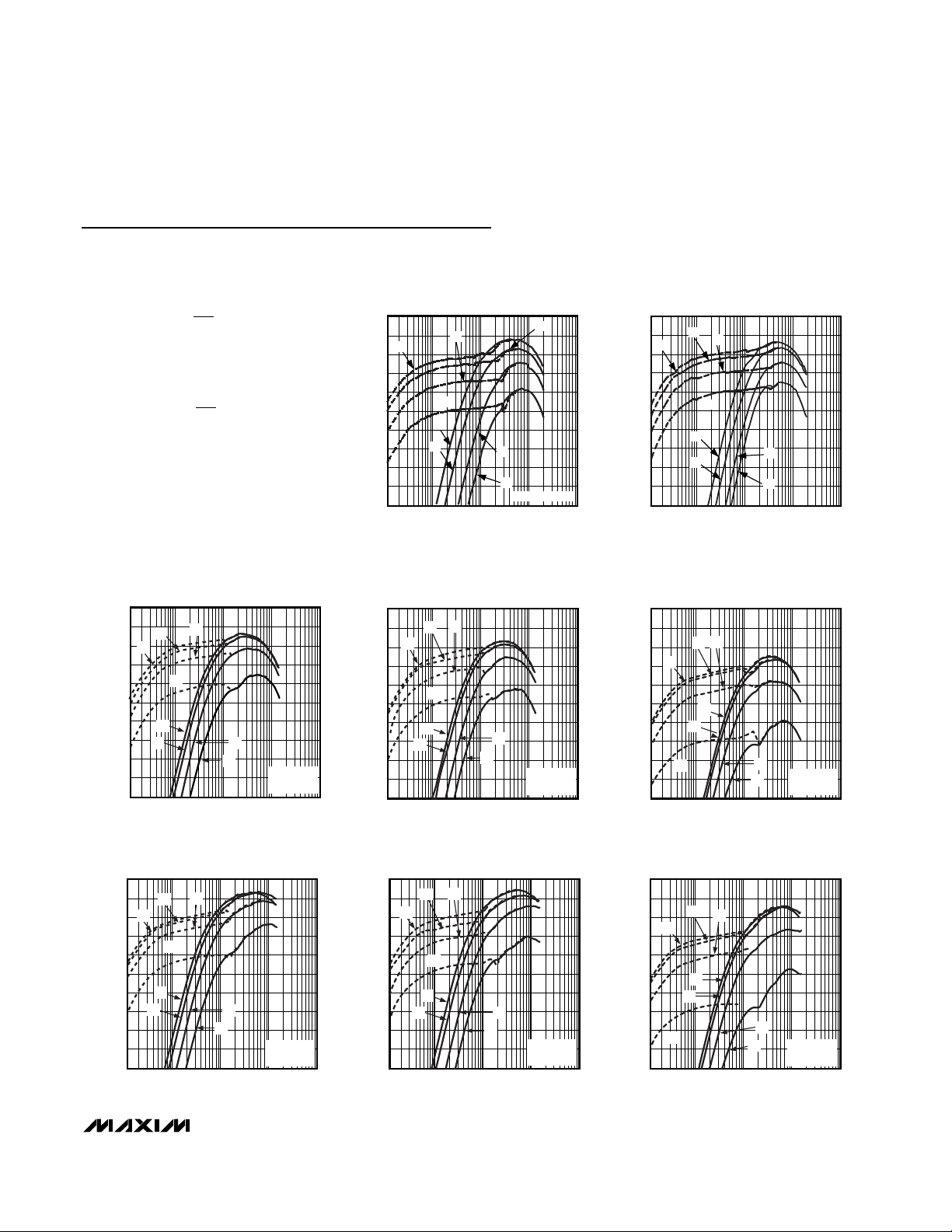
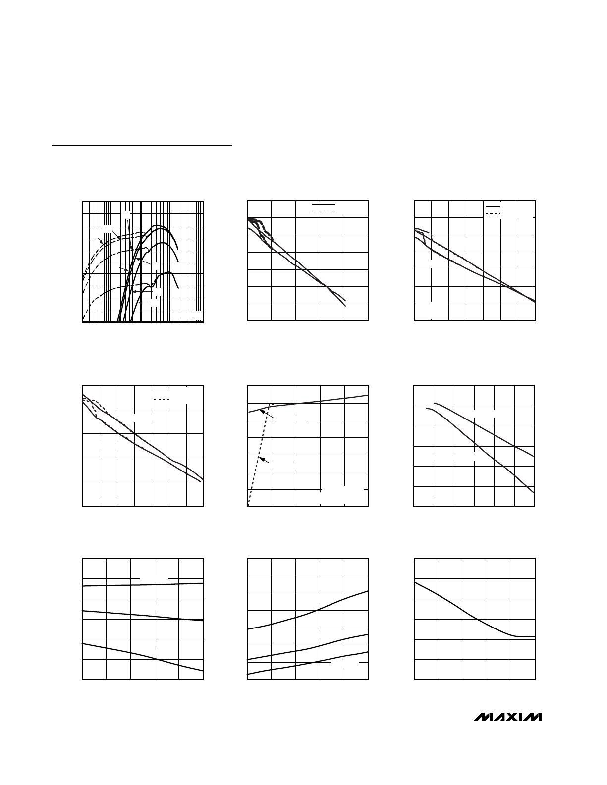
Typical Operating Characteristics
(Circuit from Figure 1, components from Table 2, TA = +25°C, unless otherwise noted.)
EFFICIENCY vs. LOAD CURRENT
(2.0V AT 300kHz)
A1
C1
D1
A2
B2
LOAD CURRENT (A)
B1
C2
D2
MAX1854 ONLY
EFFICIENCY vs.
LOAD CURRENT (1.3V AT 300kHz)
C1
B1
A1
D1
A2
B2
LOAD CURRENT (A)
C2
D2
CIRCUIT #2
L = 1.0µH
EFFECTIVE EFFICIENCY vs.
LOAD CURRENT (1.3V AT 300kHz)
C1
B1
A1
D1
A2
C2B2
D2
CIRCUIT #2
L = 1.0µH
LOAD CURRENT (A)
SKIP MODE (SKIP = GND)
A1: V
= 4.5V
BATT
= 7V
B1: V
BATT
= 15V
C1: V
BATT
= 24V
D1: V
BATT
PWM MODE (SKIP = V
A2: V
= 4.5V
BATT
= 7V
B2: V
BATT
= 15V
C2: V
BATT
= 24V
D2: V
BATT
)
CC
EFFICIENCY vs.
LOAD CURRENT (1.3V AT 200kHz)
100
95
90
A1
85
80
75
70
EFFICIENCY (%)
65
60
55
50
0.01 0.1 1 10 100
B1
D1
A2
B2
C1
C2
D2
LOAD CURRENT (A)
EFFECTIVE EFFICIENCY vs.
LOAD CURRENT (1.3V AT 200kHz)
100
95
A1
90
85
80
75
70
EFFICIENCY (%)
65
60
55
50
0.01 0.1 1 10 100
B1
D1
A2
B2
C1
C2
D2
LOAD CURRENT (A)
CIRCUIT #2
L = 1.5µH
CIRCUIT #2
L = 1.5µH
MAX1716-03
MAX1716-06
100
95
90
85
80
75
70
EFFICIENCY (%)
65
60
55
50
0.01 10.1 1 10 100
100
95
90
85
80
75
70
EFFICIENCY (%)
65
60
55
50
0.01 0.1 1 10 100
100
95
90
85
80
75
70
EFFICIENCY (%)
65
60
55
50
0.01 0.1 1 10 100
MAX1716-01
MAX1716-04
MAX1716-07
EFFICIENCY vs. LOAD CURRENT
(1.6V AT 300kHz)
100
95
90
85
80
75
70
EFFICIENCY (%)
65
60
55
50
B1
A1
0.01 10.1 1 10 100
C1
D1
A2
B2
LOAD CURRENT (A)
C2
D2
EFFICIENCY vs.
LOAD CURRENT (1.3V AT 550kHz)
100
95
90
85
80
75
70
EFFICIENCY (%)
65
60
55
50
0.01 0.1 1 10 100
A1
D1
C1
B1
A2
B2
LOAD CURRENT (A)
C2
CIRCUIT #2
D2
L = 0.68µH
EFFECTIVE EFFICIENCY vs.
LOAD CURRENT (1.3V AT 550kHz)
100
95
90
85
80
75
70
EFFICIENCY (%)
65
60
55
50
B1
A1
D1
0.01 0.1 1 10 100
C1
A2
B2
LOAD CURRENT (A)
C2
D2
CIRCUIT #2
L = 0.68µH
MAX1716-02
MAX1716-05
MAX1716-08
Page 8
MAX1716/MAX1854/MAX1855
High-Speed, Adjustable, Synchronous Step-Down
Controllers with Integrated Voltage Positioning
8 _______________________________________________________________________________________
Typical Operating Characteristics (continued)
(Circuit from Figure 1, components from Table 2, TA = +25°C, unless otherwise noted.)
EFFICIENCY vs.
LOAD CURRENT (1.0V AT 400kHz)
100
95
90
85
80
75
70
EFFICIENCY (%)
65
60
55
50
0.01 0.1 1 10 100
B1
A1
D1
C1
A2
LOAD CURRENT (A)
B2
C2
D2
CIRCUIT #3
1.64
1.62
MAX1716-09
1.60
1.58
1.56
OUTPUT VOLTAGE (V)
1.54
1.52
1.50
OUTPUT VOLTAGE vs. LOAD CURRENT
(1.6V AT 300kHz)
PWM MODE
SKIP MODE
V
= 24V
BATT
V
= 7V
BATT
010515
LOAD CURRENT (A)
20 25
1.34
MAX1716-10
1.32
1.30
1.28
1.26
OUTPUT VOTLAGE (V)
1.24
1.22
1.20
OUTPUT VOLTAGE vs.
LOAD CURRENT (1.3V AT 300kHz)
PWM MODE
SKIP MODE
V
= 24V
BATT
V
= 7V
BATT
CIRCUIT #2
L = 1.0µH
0462 8 10 12 14
LOAD CURRENT (A)
MAX1716-11
OUTPUT VOLTAGE vs.
LOAD CURRENT (1.0V AT 400kHz)
1.02
1.00
0.98
0.96
OUTPUT VOTLAGE (V)
0.94
CIRCUIT #3
0.92
0462 8 10 12 14
V
= 7V
BATT
V
= 24V
BATT
LOAD CURRENT (A)
PWM MODE
SKIP MODE
MAX1716-12
350
300
250
200
150
FREQUENCY (kHz)
100
50
0
SWITCHING FREQUENCY
vs. LOAD CURRENT
PWM MODE
SKIP MODE
V
OUT(PROG)
084 121620
LOAD CURRENT (A)
SWITCHING FREQUENCY
vs. TEMPERATURE
330
I
= 12A
320
310
300
290
SWITCHING FREQUENCY (kHz)
280
270
-40 10-15 356085
OUT
I
= 5A
OUT
I
OUT
TEMPERATURE (°C)
= 1A
MAX1716-15
0.88
0.86
0.84
0.82
0.80
ON-TIME (µs)
0.78
0.76
0.74
ON-TIME vs. TEMPERATURE
I
= 1A
OUT
I
= 5A
OUT
-40 10-15 35 60 85
TEMPERATURE (°C)
SWITCHING FREQUENCY
vs. BATTERY VOLTAGE
320
MAX1716-13
310
300
290
280
FREQUENCY (kHz)
V
= 7V
BATT
= 1.6V
270
260
V
OUT(PROG)
I
= 12A
OUT
08124 162024
V
OUT(PROG)
= 0.925V
V
BATT
= 1.6V
(V)
MAX1716 -14
NORMALIZED CURRENT-LIMIT ERROR
vs. TEMPERATURE
6
MAX1716-16
I
= 12A
OUT
4
2
0
-2
CURRENT-LIMIT ERROR (%)
-4
-6
-40 10-15 356085
TEMPERATURE (°C)
MAX1716-17
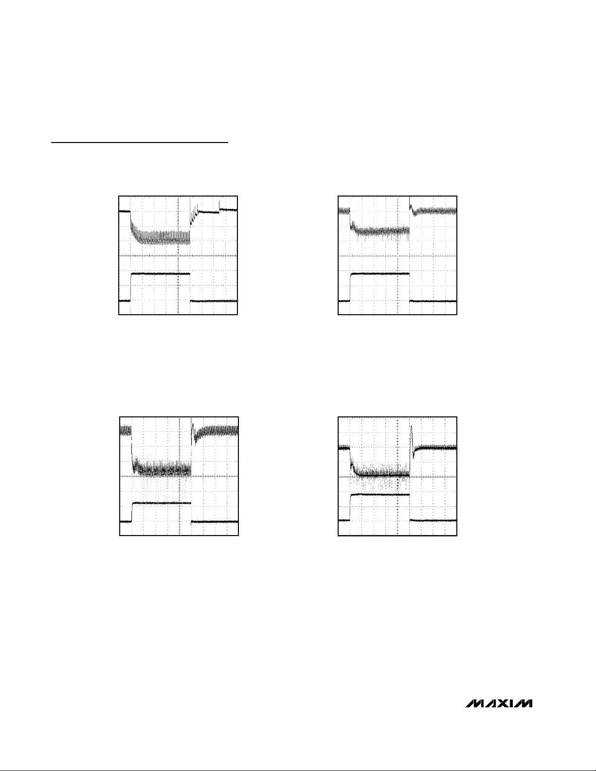
Page 9
MAX1716/MAX1854/MAX1855
High-Speed, Adjustable, Synchronous Step-Down
Controllers with Integrated Voltage Positioning
_______________________________________________________________________________________ 9
Typical Operating Characteristics (continued)
(Circuit from Figure 1, components from Table 2, TA = +25°C, unless otherwise noted.)
CURRENT-LIMIT ERROR vs. V
3
2
1
0
ERROR (%)
-1
-2
-3
0 1.0 1.50.5 2.0 2.5 3.0
(V)
V
ILIM
ILIM
MAX1716-18
NO-LOAD SUPPLY CURRENT
vs. BATTERY VOLTAGE
0.8
0.7
ICC + I
DD
MAX1716-21
0.6
0.5
0.4
CURCUIT#2 (L = 0.68µH)
SKIP MODE
550kHz (TON = GND)
0.3
SUPPLY CURRENT (mA)
0.2
0.1
I
BATT
0
084 12162024
V
(V)
BATT
LOAD-TRANSIENT RESPONSE
= 15V, PWM MODE)
(V
BATT
CONTINUOUS-TO-DISCONTINUOUS
INDUCTOR CURRENT POINT
4.5
4.0
3.5
3.0
2.5
2.0
1.5
OUTPUT CURRENT (A)
1.0
0.5
0
084 12162024
V
BATT
CIRCUIT#1
= 1.6V
V
OUT
(V)
CIRCUIT#2
= 1.3V
V
OUT
CIRCUIT#3
= 1.0V
V
OUT
NO-LOAD SUPPLY CURRENT
vs. BATTERY VOLTAGE
30
25
20
15
I
10
SUPPLY CURRENT (mA)
BATT
5
0
084 12162024
V
BATT
ICC + I
PWM MODE
550kHz (TON = GND)
CURCUIT#2 (L = 0.68µH)
(V)
DD
WITH DISABLED VOLTAGE POSITIONING
INDUCTOR CURRENT PEAKS AND
VALLEYS vs. BATTERY VOLTAGE
25
MAX1716-19
20
15
10
INDUCTOR CURRENT (A)
5
0
084 121620
NO-LOAD SUPPLY CURRENT
vs. BATTERY VOLTAGE
14
MAX1716-22
12
10
8
6
SUPPLY CURRENT (mA)
4
2
0
084 12162024
LOAD-TRANSIENT RESPONSE
I
PEAK
I
VALLEY
V
= 1.3V
OUT
CIRCUIT#2 (L = 1µH)
V
(V)
BATT
200kHz (TON = V
CURCUIT#2 (L = 1.5µH)
V
(V)
BATT
ICC + I
I
BATT
PWM MODE
MAX1716-20
24
MAX1716-23
DD
)
CC
1.60V
1.55V
1.50V
20A
10A
0
= 1.6V, 50mV/div; B. I
A. V
OUT
CIRCUIT #1, V
= 15V, PWM MODE
BATT
40µs/div
= 1.3A TO 18A, 10A/div;
OUT
MAX1716-24
A
B
1.60V
1.55V
1.50V
20A
10A
0
= 1.6V, 50mV/div; B. I
A. V
OUT
CIRCUIT #1, V
40µs/div
= 0.3A TO 18A, 10A/div;
OUT
= 15V, PWM MODE; VPS = PGND
BATT
MAX1716-25
A
B
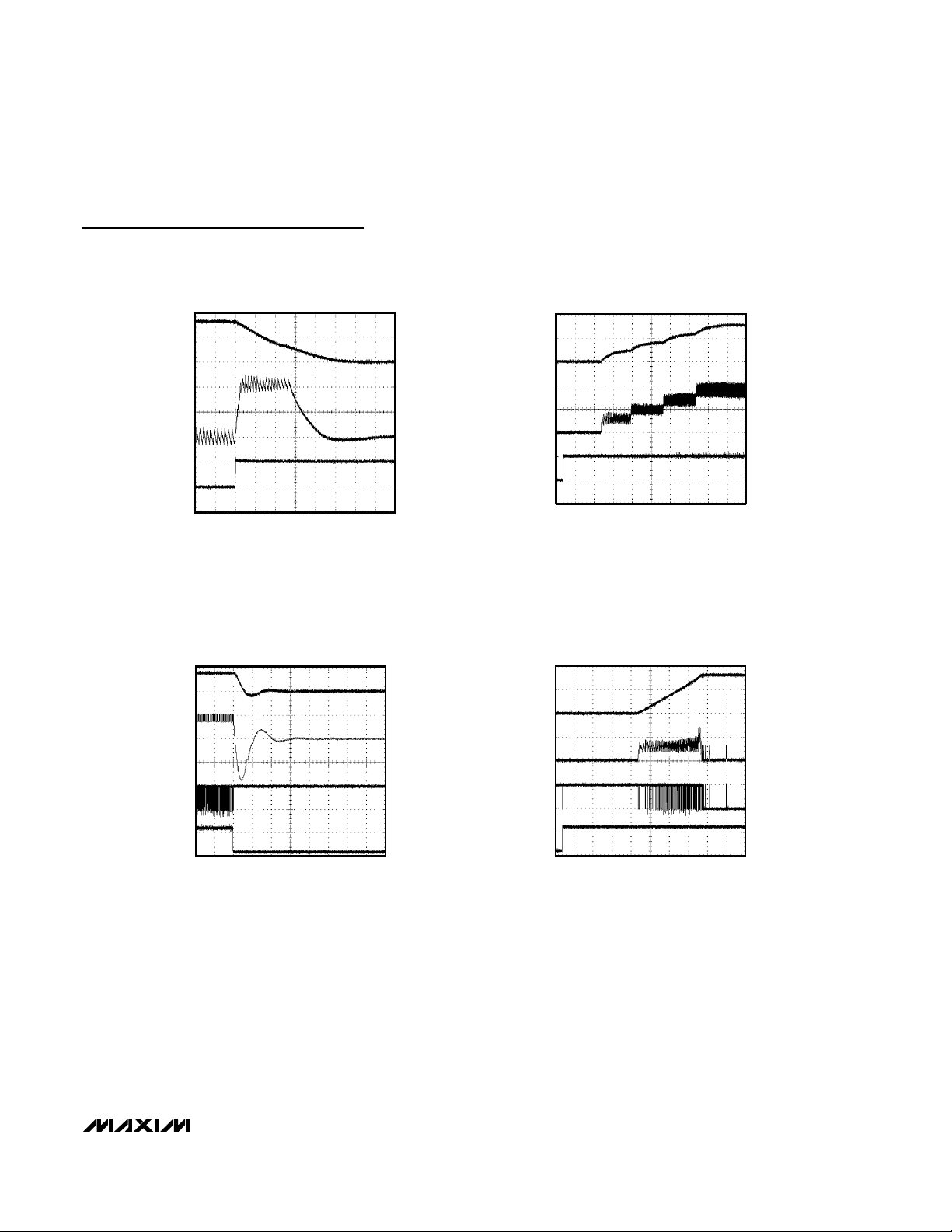
Page 10
MAX1716/MAX1854/MAX1855
High-Speed, Adjustable, Synchronous Step-Down
Controllers with Integrated Voltage Positioning
10 ______________________________________________________________________________________
Typical Operating Characteristics (continued)
(Circuit from Figure 1, components from Table 2, TA = +25°C, unless otherwise noted.)
B
10A
0
20A
1.55V
1.60V
1.50V
A
40µs/div
A. V
OUT
= 1.6V, 50mV/div; B. I
OUT
= 0.3A TO 18A, 10A/div
CIRCUIT #1, V
BATT
= 15V, SKIP MODE
LOAD-TRANSIENT RESPONSE
(V
BATT
= 15V, SKIP MODE)
MAX1716-26
LOAD-TRANSIENT RESPONSE
= 4.5V)
(V
BATT
1.60V
1.55V
1.50V
20A
10A
LOAD-TRANSIENT RESPONSE
(V
OUT(PROG)
1.00V
0.98V
0.96V
0.94V
20A
10A
0
= 1.0V)
MAX1716-28
A
B
1.65V
1.60V
1.55V
1.50V
20A
10A
0
40µs/div
= 1.6V, 50mV/div
A. V
OUT
= 0.3A TO 18A, 10A/div
B. I
OUT
CIRCUIT #1, V
= 4.5V, PWM MODE
BATT
LOAD-TRANSIENT RESPONSE
WITH CERAMIC OUTPUT CAPACITORS
0
MAX1716-27
A
B
MAX1716-29
A
B
40µs/div
= 1.0V, 20mV/div
A. V
OUT
= 0.3A TO 12A, 10A/div
B. I
OUT
CIRCUIT #3, V
= 4.5V, PWM MODE
BATT
A. V
B. I
CIRCUIT #4, V
40µs/div
= 1.6V, 50mV/div
OUT
= 0.3A TO 18A, 10A/div
OUT
= 15V, PWM MODE
BATT
Page 11
MAX1716/MAX1854/MAX1855
High-Speed, Adjustable, Synchronous Step-Down
Controllers with Integrated Voltage Positioning
______________________________________________________________________________________ 11
Typical Operating Characteristics (continued)
(Circuit from Figure 1, components from Table 2, TA = +25°C, unless otherwise noted.)
SHORT-CIRCUIT WAVEFORM
2V
1V
0
20A
10A
0
5V
0
= 1.6V, 1V/div
A. V
OUT
, L = 0.68µH, 10A/div
B. I
L
C. SHORT-CIRCUIT CONTROL, 5V/div
SHUTDOWN WAVEFORM
2V
0
20A
0
-20A
5V
0
5V
0
= 1.6V, R
A. V
OUT
, L = 0.68µH, 20A/div
B. I
L
, 5V/div
C. V
DL
= VCC TO 0, 5V/div
D. V
SHDN
20µs/div
100µs/div
= 88mΩ, 2V/div
OUT
MAX1716-30
MAX1716-32
A
B
C
A
B
C
D
2V
1V
0
20A
10A
0
5V
0
2V
1V
0
10A
0
5V
0
5V
0
STARTUP WAVEFORM
(18A LOAD)
200µs/div
A. V
= 1.6V, 1V/div
OUT
, L = 0.68µH, 10A/div
B. I
L
= 0 TO VCC, 5V/div
C. V
SHDN
= 88mΩ
R
OUT
STARTUP WAVEFORM
(NO-LOAD)
100µs/div
= 1.6V, NO LOAD, 1V/div
A. V
OUT
, L = 0.68µH, 10A/div
B. I
L
, 5V/div
C. V
DL
= 0 TO VCC, 5V/div
D. V
SHDN
MAX1716-31
A
B
C
MAX1716-33
A
B
C
D
Page 12

MAX1716/MAX1854/MAX1855
High-Speed, Adjustable, Synchronous Step-Down
Controllers with Integrated Voltage Positioning
12 ______________________________________________________________________________________
Pin Description
PIN NAME FUNCTION
1 DH High-Side Gate Driver Output. DH swings from LX to BST.
2V+
3 SHDN
4FB
5CC
6 ILIM
7V
8TON
9 REF
10 GND Analog Gound
CC
Battery Voltage Sense Connection. Connect V+ to input power source. V+ is used only for PWM
one-shot timing. DH on-time is inversely proportional to input voltage over a 2V to 28V range.
Shutdown Control Input. Drive SHDN to GND to force the MAX1716/MAX1854/MAX1855 into
shutdown. Drive or connect to VCC for normal operation. A rising edge on SHDN clears the fault
latch.
Feedback Input. Normally connected to V
locally at the power supply. An external resistive divider can optionally set the output voltage.
Voltage-Positioning Compensation Capacitor. Connect a 47pF to 1000pF (47pF typ) capacitor from
CC to GND to adjust the loop’s response time.
Current-Limit Adjustment. The GND-CS current-limit threshold defaults to 120mV, if ILIM is tied to
. In adjustable mode, the current-limit threshold voltage is 1/10th the voltage seen at ILIM over a
V
CC
0.5V to 2.0V range. The logic threshold for switchover to the 120mV default value is approximately
V
- 1V. Connect ILIM to REF for a fixed 200mV threshold.
CC
Analog Supply Input for PWM Core. Connect to the system supply voltage (+4.5V to +5.5V) with a
series 20Ω resistor. Bypass to GND with a 0.22µF (min) ceramic capacitor.
On-Time Selection-Control Input. This is a four-level input used to determine DH on-time. Connect to
GND, REF, or V
550kHz, REF = 400kHz, floating = 300kHz, and V
+2.0V Reference Voltage Output. Bypass to GND with 0.22µF (min) capacitor. Can supply 50µA for
external loads.
, or leave TON unconnected to set the following switching frequencies: GND =
CC
OUT
. FB is connected to the bulk output filter capacitors
= 200kHz.
CC
Voltage-Positioning Sense Input. Connect to CS through a 1kΩ resistor to maximize the load-
11 VPS
12 VGATE
13 DL Low-Side Gate-Driver Output. DL swings from PGND to VDD.
14 PGND Power Ground
15 V
16 D4 MSB DAC Code Input. 5µA internal pullup to VCC (Table 5).
17 D3 DAC Code Input. 5µA internal pullup to VCC (Table 5).
18 D2 DAC Code Input. 5µA internal pullup to VCC (Table 5).
19 D1 DAC Code Input. 5µA internal pullup to VCC (Table 5).
20 D0 LSB DAC Code Input. 5µA internal pullup to VCC (Table 5).
DD
dependent output voltage drop, or adjust the voltage positioning level by connecting a resistive
divider from CS to PGND. Refer to Setting Voltage Positioning on how to select resistor values.
Open-Drain Power-Good Output. VGATE is normally high when the output is in regulation. VGATE is
low in shutdown, undervoltage lockout, and during soft-start. Any fault condition forces VGATE low,
and it remains low until the fault is cleared.
Supply Input for the DL Gate Drive. Connect to the system supply voltage, +4.5V to +5.5V. Bypass
to PGND with a 1µF (min) ceramic capacitor.
Page 13

MAX1716/MAX1854/MAX1855
High-Speed, Adjustable, Synchronous Step-Down
Controllers with Integrated Voltage Positioning
______________________________________________________________________________________ 13
Pin Description (continued)
Table 1. Component Selection for Standard Applications
PIN NAME FUNCTION
Pulse-Skipping or Low-Noise Mode Control Input. Connect to V
Connect to GND to enable pulse-skipping operation. Low-noise forced-PWM mode causes inductor
21 SKIP
22 BST
23 LX
24 CS
COMPONENT
Output Voltage 1.6V 1.3V 1.0V 1.6V
Input Voltage Range 7V to 24V 7V to 24V 7V to 24V 7V to 24V
M axi m um Load C ur r ent 18A 12A 12A 18A
Inductor
TON Level Float Float REF GND
Frequency 300kHz 300kHz 400kHz 550kHz
High-Side MOSFET
Low-Side MOSFET
current recirculation at light loads and suppresses pulse-skipping operation. Normal operation
prevents current recirculation. SKIP can also be used to disable both overvoltage and undervoltage
protection circuits and clear the fault latch (see No-Fault Test Mode). Do not leave SKIP floating.
Boost Flying-Capacitor Connection. Connect to an external capacitor and diode according to the
standard application circuit (Figure 1).
External Inductor Connection. Connect LX to the switched side of the inductor. LX serves as the
lower supply rail for the DH high-side gate driver. LX does not connect to the current-limit
comparator.
Current-Sense Input. Connect a resistor (R
threshold is set by ILIM. If the current-sense signal (Inductor Current
current-limit threshold, the MAX1716/MAX1854/MAX1855 will not initiate a new cycle.
CIRCUIT 1
(FIGURE 1)
0.68µH
Sumida
CDEP134H-0R6
or Panasonic
ETQP6F0R6BFA
International Rectifier
(2) IRF7811
Fairchild (2) FDS7764A
Or International
Rectifier (2) IRF7811
CIRCUIT 2
(FIGURE 11)
1µH
Sumida
CEP125-1R0MC
or Panasonic
ETQP6FIRIBFA
International Rectifier
IRF7811
Fairchild (2) FDS7764A
Or International
Rectifier (2) IRF7811
SENSE
for low-noise forced-PWM mode.
CC
) between CS and PGND. The current-limit
✕ R
CIRCUIT 3
(FIGURE 12)
0.68µH
Sumida
CDEP134H-0R6
or Panasonic
ETQP6F0R6BFA
International Rectifier
IRF7811
Fairchild (2) FDS7764A
Or International
Rectifier (2) IRF7811
) exceeds the
SENSE
CIRCUIT 4
(FIGURE 13)
0.47µH
Sumitomo
CXE-R47
International Rectifier
(2) IRF7811
Fairchild (2) FDS7764A
Or International
Rectifier (2) IRF7811
(5) 10µF
Input Capacitor
Output Capacitor
Current-Sense Resistor 3mΩ 3.5mΩ 3.5mΩ 3mΩ
ILIM Level V
Voltage-Positioning
Resistor Ratio
Taiyo Yuden
TMK432BJ106
(5) 220µF
Panasonic
EEFUE0E221R
/3 V
REF
1:1 (0.5x) 1:2 (0.66x) 1:2 (0.66x) 1:1 (0.5x)
(4) 10µF
Taiyo Yuden
TMK432BJ106
(4) 220µF
Panasonic
EEFUE0E221R
/4 V
REF
(4) 10µF
Taiyo Yuden
TMK432BJ106
(4) 220µF
Panasonic
EEFUE0E221R
/4 V
REF
(5) 10µF
Taiyo Yuden
TMK432BJ106
(8) 47µF
Taiyo Yuden
JMK432BJ476MM
or TDK
C4532X5ROJ476M
REF
/3
Page 14

MAX1716/MAX1854/MAX1855
High-Speed, Adjustable, Synchronous Step-Down
Controllers with Integrated Voltage Positioning
14 ______________________________________________________________________________________
_______________Detailed Description
The MAX1716/MAX1854/MAX1855 buck controllers are
targeted for low-voltage, high-current CPU core power
supplies for notebook computers that typically require
18A (or greater) load steps. The proprietary QuickPWM pulse-width modulator in the converter is specifically designed for handling fast load steps while
maintaining a relatively constant operating frequency
and inductor operating point over a wide range of input
voltages. The Quick-PWM architecture circumvents the
poor load-transient timing problems of fixed-frequency
current-mode PWMs while also avoiding the problems
caused by widely varying switching frequencies in conventional constant on-time and constant off-time PFM
schemes.
+5V Bias Supply (VCCand VDD)
The MAX1716/MAX1854/MAX1855 require an external
+5V bias supply in addition to the battery. Typically this
+5V bias supply is the notebook’s 95% efficient +5V
system supply. Keeping the bias supply external to the
IC improves efficiency and eliminates the cost associated with the +5V linear regulator that would otherwise be
needed to supply the PWM circuit and gate drivers. If
stand-alone capability is needed, the +5V supply can
be generated with an external linear regulator.
The +5V bias supply powers V
CC
(PWM controller) and
VDD(gate-drive power). The maximum current is:
I
BIAS
= ICC+ ƒ × (QG1+ QG2) = 10mA to 40mA (typ)
where ICCis 700µA (typ), ƒ is the switching frequency,
and QG1and QG2are the MOSFET data sheet total
gate-charge specification limits at VGS= 5V.
The battery input (V+) and +5V bias inputs (VCCand
V
DD
) can be connected together if the input source is a
fixed 4.5V to 5.5V supply. If the +5V bias supply is
powered up prior to the battery supply, the enable signal (SHDN) must be delayed until the battery voltage is
present to ensure startup.
Free-Running, Constant-On-Time PWM
Controller with Input Feed-Forward
The Quick-PWM control architecture is a constant-ontime, current-mode type with voltage feed-forward
(Figure 2). This architecture relies on the output ripple
voltage to provide the PWM ramp signal. Thus, the output filter capacitor’s ESR acts as a feedback resistor.
The control algorithm is simple: the high-side switch ontime is determined solely by a one-shot whose period is
inversely proportional to input voltage and directly proportional to output voltage (see On-Time One-Shot).
Another one-shot sets a minimum off-time (400ns typ).
The on-time one-shot is triggered if the error compara-
Table 2. Component Suppliers
MANUFACTURER PHONE (COUNTRY CODE) WEBSITE
MOSFETs
Fairchild Semiconductor (1) 888-522-5372 www.fairchildsemi.com
International Rectifier (1) 310-322-3331 www.irf.com
Siliconix (1) 203-268-6261 www.vishay.com
CAPACITORS
Kemet (1) 408-986-0424 www.kemet.com
Panasonic (1) 847-468-5624 www.panasonic.com
Sanyo
Taiyo Yuden
TDK (1) 847-390-4373 www.tdk.com
INDUCTORS
Coilcraft (1) 800-322-2645 www.coilcraft.com
Coiltronics (1) 561-752-5000 www.coiltronics.com
Sumida (1) 408-982-9660 www.sumida.com
Sumitomo
(65) 281-3226 (Singapore)
(1) 408-749-9714
(03) 3667-3408 (Japan)
(1) 408-573-4150
(1) 408-451-8441 (USA)
81 75 961-3141 (Japan)
www.secc.co.jp
www.t-yuden.com
www.ssmc.co.jp
Page 15
MAX1716/MAX1854/MAX1855
High-Speed, Adjustable, Synchronous Step-Down
Controllers with Integrated Voltage Positioning
______________________________________________________________________________________ 15
tor is low, the low-side switch current is below the current-limit threshold, and the minimum off-time one-shot
has timed out.
On-Time One-Shot (TON)
The heart of the PWM core is the one-shot that sets the
high-side switch on-time. This fast, low-jitter, adjustable
one-shot includes circuitry that varies the on-time in
response to the input and output voltages. The highside switch on-time is inversely proportional to V+, and
directly proportional to the output voltage as set by the
DAC code. This algorithm results in a nearly constant
switching frequency despite the lack of a fixed-frequency clock generator. The benefits of a constant switching frequency are twofold: first, the frequency can be
selected to avoid noise-sensitive regions, such as the
455kHz IF band; second, the inductor ripple-current
operating point remains relatively constant, resulting in
easy design methodology and predictable output voltage ripple.
On-Time = K × (V
OUT
+ 75mV) / V+
where K is set by the TON pin-strap connection, and
75mV is an approximation to accommodate for the
expected drop across the low-side MOSFET switch and
current-sense resistor (Table 3).
The on-time one-shot has good accuracy at the operating points specified in the Electrical Characteristics
table. On-times at operating points far removed from
the conditions specified in the Electrical Characteristics
table can vary over a wide range. For example, the
550kHz setting will typically run about 10% slower with
inputs much greater than the +5V due to the very short
on-times required.
While the on-time is set by TON, V+, and the output
voltage, other factors also contribute to the overall
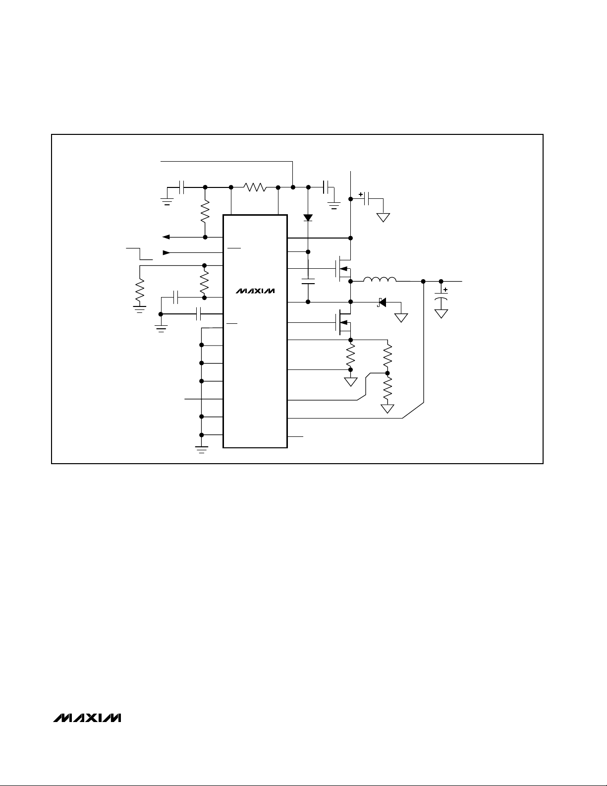
Figure 1. Standard High-Power Application (Circuit #1)
+5V INPUT
BIAS SUPPLY
POWER-GOOD
INDICATOR
ON OFF
R6
100kΩ
C5
1µF
0.22µF
TO V
R3
10Ω
R4
100kΩ
R5
C1
200kΩ
C2
47pF
CC
V
CC
VGATE
SHDN
ILIM
REF
CC
SKIP
D0
D1
D2
D3
D4
GND
MAX1716
MAX1854
MAX1855
V
DD
BST
PGND
VPS
TON
V+
DH
LX
DL
CS
FB
D1
C3
0.1µF
FLOAT (300kHz)MAX1716 DAC CODE SHOWN
C4
1µF
BATTERY (V
7V TO 24V
C
IN
(5) 10µF
Q1
0.68µH
Q2
R
SENSE
3mΩ
L1
BATT
D2
)
R1
1kΩ
R2
1kΩ
Q1: (2) IRF7811
INTERNATIONAL RECTIFIER
Q2: (2) IRF7811
INTERNATIONAL RECTIFIER
D1: CMPSH-3
CENTRAL SEMICONDUCTOR
D2: CMSH2-60
CENTRAL SEMICONDUCTOR
1.6V OUTPUT
UP TO 18A
C
OUT
(5) 220µF
PANASONIC
Page 16

MAX1716/MAX1854/MAX1855
High-Speed, Adjustable, Synchronous Step-Down
Controllers with Integrated Voltage Positioning
16 ______________________________________________________________________________________
Figure 2. Functional Diagram
Table 3. Approximate K-Factor Errors
IN
2V TO 28V
REF
V+
TOFF
AMP
Q
*
OVP/UVP
DETECT
1-SHOT
S
R
TRIG
Q
CURRENT
LIMIT
Σ
S
Q
R
x2
R-2R
DAC
TON
SKIP
SHDN
CC
VPS
VGATE
gm
TRIG
ON-TIME
COMPUTE
1-SHOT
TON
TON
-10%
REF
Q
200k
FROM
OUT
REF
7R R
REF
+10%
ERROR
I
LIM
9R
R
MAX1716
MAX1854
MAX1855
ZERO CROSSING
CHIP
SUPPLY
REF
+5V
BST
DH
LX
CS
+5V
V
DD
DL
PGND
FB
V
CC
2V
REF
+5V
OUTPUT
CS
D0
D1 D2 D3 D4
NO OVERVOLTAGE PROTECTION ON THE MAX1854
*
TON SETTING
(kHz)
K-FACTOR
(µs)
APPROXIMATE
K-FACTOR ERROR (%)
MIN RECOMMENDED V
V
= 1.6V (V)
OUT
200 5 ±9 2.04
300 3.3 ±11 2.28
400 2.2 ±15 2.84
550 1.8 ±20 3.55
BATT
AT
Page 17

MAX1716/MAX1854/MAX1855
High-Speed, Adjustable, Synchronous Step-Down
Controllers with Integrated Voltage Positioning
______________________________________________________________________________________ 17
switching frequency. The on-time guaranteed in the
Electrical Characteristics table is influenced by switching delays in the external high-side MOSFET. Resistive
losses—including the inductor, both MOSFETs, output
capacitor ESR, and PC board copper losses in the output and ground—tend to raise the switching frequency
at higher output currents. Switch dead-time can
increase the effective on-time, reducing the switching
frequency. This effect occurs only in PWM mode (SKIP
= high) when the inductor current reverses at light or
negative load currents. With reversed inductor current,
the inductor’s EMF causes LX to go high earlier than
normal, extending the on-time by a period equal to the
DH-rising dead-time.
When the controller operates in continuous mode, the
dead-time is no longer a factor and the actual switching
frequency is:
ƒ = (V
OUT
+ V
DROP1
) / [tON× (V+ + V
DROP1
– V
DROP2
)]
where V
DROP1
is the sum of the parasitic voltage drops
in the inductor discharge path, including synchronous
rectifier, inductor, and PC board resistances; V
DROP2
is
the sum of the resistances in the charging path, including high-side switch, inductor, and PC board resistances; and tONis the on-time calculated by the
MAX1716/MAX1854/MAX1855.
Automatic Pulse-Skipping Switchover
In skip mode (SKIP = low), an inherent automatic
switchover to PFM takes place at light loads (Figure 3).
This switchover is controlled by a comparator that truncates the low-side switch on-time at the inductor current’s zero crossing. This mechanism causes the
threshold between pulse-skipping PFM and nonskipping PWM operation to coincide with the boundary
between continuous and discontinuous inductor-current operation. For an input voltage (V+) range of 7V to
24V, this threshold is relatively constant, with only a
minor dependence on the input voltage:
where K is the on-time scale factor (Table 3). The loadcurrent level at which PFM/PWM crossover occurs,
I
LOAD(SKIP)
, is equal to 1/2 the peak-to-peak ripple current, which is a function of the inductor value (Figure 3).
For example, in the standard application circuit with
K = 3.3µs (300kHz), V
BATT
= 12V, V
OUT
= 1.6V, and
L = 0.68µH, switchover to pulse-skipping operation
occurs at I
LOAD
= 2.3A or about 1/4 full load. The
crossover point occurs at an even lower value if a
swinging (soft-saturation) inductor is used.
The switching waveforms may appear noisy and asynchronous when light loading causes pulse-skipping
operation; this is a normal operating condition that
improves light-load efficiency. Trade-offs in PFM noise
vs. light-load efficiency are made by varying the inductor value. Generally, low inductor values produce a
broader efficiency vs. load curve, while higher values
result in higher full-load efficiency (assuming that the
coil resistance remains fixed) and less output voltage
ripple. Penalties for using higher inductor values
include larger physical size and degraded load-transient response (especially at low input voltage levels).
Forced-PWM Mode (
SSKKIIPP
= High)
The low-noise, forced-PWM mode (SKIP driven high)
disables the zero-crossing comparator that controls the
Figure 4. “Valley” Current-Limit Threshold Point
Figure 3. Pulse-Skipping/Discontinuous Crossover Point
∆i
∆t
INDUCTOR CURRENT
- V
V
BATT
=
ON-TIME0 TIME
OUT
L
-I
PEAK
I
= I
PEAK
/2
LOAD
-I
PEAK
INDUCTOR CURRENT
0 TIME
I
LOAD SKIP
()
KVLVV
×
≈
OUT OUT
2
+−
I
LOAD
I
LIMIT
V
+
Page 18

MAX1716/MAX1854/MAX1855
High-Speed, Adjustable, Synchronous Step-Down
Controllers with Integrated Voltage Positioning
18 ______________________________________________________________________________________
low-side switch on-time. The resulting low-side gatedrive waveform is forced to be the complement of the
high-side gate-drive waveform. This, in turn causes the
inductor current to reverse at light loads, as the PWM
loop strives to maintain a duty ratio of V
OUT
/V+. The
benefit of forced-PWM mode is to keep the switching
frequency nearly constant, but it results in higher noload supply current that can be 10mA to 40mA,
depending on the external MOSFETs and switching frequency.
Forced-PWM mode is most useful for minimizing audiofrequency noise and improving the cross-regulation of
multiple-output applications that use a flyback transformer or coupled inductor.
Current-Limit Circuit (ILIM)
The current-limit circuit employs a unique “valley” current-sensing algorithm. If the current-sense signal is
above the current-limit threshold, the MAX1716/
MAX1854/MAX1855 will not initiate a new cycle (Figure
4). The actual peak current is greater than the currentlimit threshold by an amount equal to the inductor ripple current. Therefore, the exact current-limit
characteristic and maximum load capability are a function of the current-limit threshold, inductor value, and
input voltage. The reward for this uncertainty is robust,
loss-less overcurrent sensing. When combined with the
UVP protection circuit, this current-limit method is effective in almost every circumstance.
There is also a negative current limit that prevents
excessive reverse inductor currents when V
OUT
is sinking current. The negative current-limit threshold is set to
approximately 120% of the positive current limit and
therefore tracks the positive current limit when ILIM is
adjusted.
The MAX1716/MAX1854/MAX1855 measure the current
by sensing the voltage between CS and PGND.
Connect an external sense resistor between the source
of the low-side N-channel MOSFET and PGND. This
same resistor is also used to generate the input voltage
for the VPS input (see Setting Voltage Positioning).
Reducing the sense voltage increases the relative measurement error. However, the configuration eliminates
the uncertainty of using the low-side MOSFET on-resistance to measure the current, so the resulting currentlimit tolerance is tighter when sensing with a 1% sense
resistor.
In some applications, the signal required for voltage
positioning is much smaller than the minimum currentlimit voltage (50mV). There are two options for addressing this issue. One method is to use a larger
current-sense resistor to develop the appropriate current-limit voltage and divide down this signal to obtain
the desired VPS input. This solution provides the maximum current-limit accuracy. Alternatively, select a
sense resistance to generate the desired VPS voltage
and connect CS to LX. This results in minimum powerdissipation with reduced current-limit accuracy. The
default 120mV current limit (ILIM = V
CC
) accommodates current-limit detection using the low-side power
MOSFET and low-value sense resistor.
The voltage at ILIM sets the current-limit threshold. For
voltages from 500mV to 2V, the current-limit threshold
voltage is precisely 0.1 × V
ILIM
. Set this voltage with a
resistive divider between REF and GND. The currentlimit threshold defaults to 120mV when ILIM is tied to
X = Don’t care
Table 4. Operating Mode Truth Table
SHDN SKIP DL MODE COMMENTS
0 X High Shutdown Micropower shutdown state.
1 GND Switching
1VCCSwitching Forced PWM
Normal
Operation
Automatic switchover from PWM mode to pulse-skipping
PFM mode at light loads. Prevents inductor current from
recirculating into the input.
Low-noise forced-PWM mode causes inductor current to
reverse at light loads and suppresses pulse-skipping
operation.
Test mode with overvoltage, undervoltage, and thermal
shutdown faults disabled. Otherwise, the converter
operates as if SKIP = GND.
No-Fault Test
Mode
1 Below GND Switching
Page 19

MAX1716/MAX1854/MAX1855
High-Speed, Adjustable, Synchronous Step-Down
Controllers with Integrated Voltage Positioning
______________________________________________________________________________________ 19
VCC. The logic threshold for switchover to the 120mV
default value is approximately VCC- 1V.
Carefully observe the PC board layout guidelines to
ensure that noise and DC errors don’t corrupt the current-sense signals seen by CS and PGND. The IC must
be mounted close to the current-sense resistor with
short, direct traces making a Kelvin sense connection.
MOSFET Gate Drivers (DH and DL)
The DH and DL drivers are optimized for driving moderate-sized, high-side and larger, low-side power
MOSFETs. This is consistent with the low duty factor
seen in the notebook CPU environment, where a large
VIN- V
OUT
differential exists. An adaptive dead-time
circuit monitors the DL output and prevents the highside FET from turning on until DL is fully off. There must
be a low-resistance, low-inductance path from the DL
driver to the MOSFET gate in order for the adaptive
dead-time circuit to work properly. Otherwise, the
sense circuitry in the MAX1716/MAX1854/MAX1855 will
interpret the MOSFET gate as “off” while there is actually still charge left on the gate. Use very short, wide
traces measuring 10 to 20 squares (50 to 100 mils wide
if the MOSFET is 1 inch from the device). The dead
time at the other edge (DH turning off) is determined by
a fixed 35ns internal delay.
The internal pulldown transistor that drives DL low is
robust, with a 0.5Ω (typ) on-resistance. This helps prevent DL from being pulled up during the fast rise time
of the LX node, due to capacitive coupling from the
drain to the gate of the low-side synchronous-rectifier
MOSFET. However, for high-current applications, some
combinations of high- and low-side FETs may cause
excessive gate-drain coupling, leading to poor efficiency, EMI, and shoot-through currents. This is often remedied by adding a resistor in series with BST, which
increases the turn-on time of the high-side FET without
degrading the turn-off time (Figure 5).
DAC Converter (D0–D4)
The digital-to-analog converter (DAC) programs the
output voltage. It receives a preset digital code from
the VID inputs (D0–D4), which contain weak internal
pullups to eliminate external resistors. They can also be
driven by digital logic, general-purpose I/O, or an external multiplexer. The available DAC codes and resulting
output voltages (Table 5) are compatible with Intel’s
mobile Pentium III™ specifications.
D0-D4 can be changed while the regulator is active, initiating a transition to a new output voltage level.
Change D0–D4 synchronously to avoid errors during a
V
OUT
transition. If the skew between bits exceeds 1µs,
incorrect DAC outputs may cause a partial transition to
the wrong voltage level, followed by the intended transition to the correct voltage level, lengthening the overall transition time.
When changing the MAX1855 DAC code while powered up, the undervoltage protection feature can be
activated if the code change increases the output voltage by more than 120%. For example, a transition from
any DAC code below 0.8V to 1.75V will activate the
undervoltage protection. In the preceding example,
transitioning from 0.8V to 1.35V and then from 1.35V to
1.75V avoids activating the undervoltage protection
feature.
Shutdown (
SSHHDDNN
)
Drive SHDN low to force the MAX1716/MAX1854/
MAX1855 into a low-current shutdown state. Shutdown
turns on the low-side MOSFET by forcing the DL gate
driver high, which discharges the output capacitor and
forces the output to ground. Drive or connect SHDN to
VCCfor normal operation. A rising edge on SHDN
clears the fault latch.
Power-on Reset
Power-on reset (POR) occurs when VCCrises above
approximately 2V. This resets the fault latch and softstart counter, preparing the regulator for operation.
Figure 5. Reducing the Switching-Node Rise Time
Pentium III is a trademark of Intel Corp.
+5V
5Ω TYP
BST
DH
LX
MAX1716
MAX1854
MAX1855
V
BATT
Page 20

MAX1716/MAX1854/MAX1855
High-Speed, Adjustable, Synchronous Step-Down
Controllers with Integrated Voltage Positioning
20 ______________________________________________________________________________________
Undervoltage Lockout and Soft-Start
VCCundervoltage lockout (UVLO) circuitry inhibits
switching, forces VGATE low, and drives the DL output
high. If the V
CC
voltage drops below 4.2V, it is
assumed that there is not enough supply voltage to
make valid decisions. To protect the output from overvoltage faults, DL is forced high in this mode. This will
force the output to GND and results in large negative
inductor current that pulls the output below GND. If V
CC
is likely to drop in this fashion, the output can be
*Note: In the no-CPU state, DH and DL are held low.
Table 5. Output Voltage vs. DAC Codes
D4 D3 D2 D1 D0
00000 No CPU* 2.000V 1.750V
00001 No CPU* 1.950V 1.700V
00010 No CPU* 1.900V 1.650V
00011 No CPU* 1.850V 1.600V
00100 No CPU* 1.800V 1.550V
00101 No CPU* 1.750V 1.500V
00110 No CPU* 1.700V 1.450V
00111 No CPU* 1.650V 1.400V
01000 1.600V 1.600V 1.350V
01001 1.550V 1.550V 1.300V
01010 1.500V 1.500V 1.250V
01011 1.450V 1.450V 1.200V
01100 1.400V 1.400V 1.150V
01101 1.350V 1.350V 1.100V
01110 1.300V 1.300V 1.050V
01111 No CPU* No CPU* 1.000V
10000 1.275V 1.275V 0.975V
10001 1.250V 1.250V 0.950V
10010 1.225V 1.225V 0.925V
10011 1.200V 1.200V 0.900V
10100 1.175V 1.175V 0.875V
10101 1.150V 1.150V 0.850V
10110 1.125V 1.125V 0.825V
10111 1.100V 1.100V 0.800V
11000 1.075V 1.075V 0.775V
11001 1.050V 1.050V 0.750V
11010 1.025V 1.025V 0.725V
11011 1.000V 1.000V 0.700V
11100 0.975V 0.975V 0.675V
11101 0.950V 0.950V 0.650V
11110 0.925V 0.925V 0.625V
11111 No CPU* No CPU* 0.600V
MAX1716 MAX1854 MAX1855
OUTPUT VOLTAGE
Page 21

MAX1716/MAX1854/MAX1855
High-Speed, Adjustable, Synchronous Step-Down
Controllers with Integrated Voltage Positioning
______________________________________________________________________________________ 21
clamped with a Schottky diode to GND to reduce the
negative excursion.
To ensure correct startup, V+ should be present before
VCC. If the converter attempts to bring the output into
regulation without V+ present, the fault latch will trip.
After VCCrises above 4.2V, an internal digital soft-start
timer begins to ramp up the maximum allowed current
limit. The ramp occurs in five steps: 20%, 40%, 60%,
80%, and 100%, with 100% load current available after
1.7ms ±50%.
Power-Good Output (VGATE)
VGATE is the open-drain output of a window comparator. This power-good output remains high impedance
as long as the output voltage is within ±10% of the regulation voltage. When the output voltage is greater than
or less than the ±10% window limits, the internal MOSFET is activated and pulls the output low. Any fault condition forces VGATE low until the fault is cleared.
VGATE is also low in shutdown, undervoltage lockout,
and during soft-start. For logic-level output voltages,
connect an external pullup resistor between VGATE
and VCC(or VDD). A 100kΩ resistor works well in most
applications.
Output Overvoltage Protection
(MAX1716/MAX1855 only)
The overvoltage protection (OVP) circuit is designed to
protect against a shorted high-side MOSFET by drawing high current and activating the battery’s protection
circuit. The output voltage is continuously monitored for
overvoltage. If the output exceeds the OVP threshold
(1.9V with the MAX1716, 2.0V with the MAX1855), OVP
is triggered and the circuit shuts down. The DL lowside gate-driver output latches high until SHDN toggles
or V
CC
pulses below 1V. This action turns on the synchronous-rectifier MOSFET with 100% duty cycle and,
in turn, rapidly discharges the output filter capacitor,
forcing the output to ground. If the condition that
caused the overvoltage (such as a shorted high-side
MOSFET) persists, the battery’s internal protection circuit will engage.
OVP can be defeated through the no-fault test mode
(see No-Fault Test Mode).
Output Undervoltage Protection
The output undervoltage protection (UVP) function is
similar to foldback current limiting, but employs a timer
rather than a variable current limit. If the regulator’s output voltage is under 40% of the nominal value, anytime
after the 20ms undervoltage fault-blanking time, the
PWM is latched off and won’t restart until SHDN toggles
or VCCpulses below 1V.
UVP can be defeated through the no-fault test mode
(see No-Fault Test Mode).
Thermal Fault Protection
The MAX1716/MAX1854/MAX1855 feature a thermal
fault protection circuit. When the temperature rises
above +150°C, the DL low-side gate-driver output
latches high until SHDN toggles or VCCpulses below
1V. The threshold has +10°C of thermal hysteresis,
which prevents the regulator from restarting until the
die cools off.
No-Fault Test Mode
The over/undervoltage protection features can complicate the process of debugging prototype breadboards
since there are at most a few milliseconds in which to
determine what went wrong. Therefore, a test mode is
provided to disable the OVP, UVP, and thermal shutdown features, and clear the fault latch if it has been
set. The PWM operates as if SKIP were low (SKIP
mode).
The no-fault test mode is entered by sinking 1.5mA
from SKIP through an external negative voltage source
in series with a resistor. SKIP is clamped to GND with a
silicon diode, so choose the resistor value equal to
(V
FORCE
- 0.65V) / 1.5mA.
Design Procedure
Firmly establish the input voltage range and maximum
load current before choosing a switching frequency
and inductor operating point (ripple-current ratio). The
primary design trade-off lies in choosing a good switching frequency and inductor operating point. The following four factors dictate the design:
Input voltage range: The maximum value (V+
(MAX)
)
must accommodate the worst-case high AC-adapter
voltage. The minimum value (V+
(MIN)
) must account for
the lowest input voltage after drops due to connectors,
fuses, and battery selector switches. If there is a choice
at all, lower input voltages result in better efficiency.
Maximum load current: There are two values to consider. The peak load current (I
LOAD(MAX)
) determines
the instantaneous component stresses and filtering
requirements, and thus drives output capacitor selection, inductor saturation rating, and the design of the
current-limit circuit. The continuous load current
(I
LOAD
) determines the thermal stresses and thus drives the selection of input capacitors, MOSFETs, and
other critical heat-contributing components. Modern
notebook CPUs generally exhibit I
LOAD
= I
LOAD(MAX)
×
80%.
Switching frequency: This choice determines the
basic trade-off between size and efficiency. The opti-
Page 22

MAX1716/MAX1854/MAX1855
High-Speed, Adjustable, Synchronous Step-Down
Controllers with Integrated Voltage Positioning
22 ______________________________________________________________________________________
mal frequency is largely a function of maximum input
voltage, due to MOSFET switching losses that are proportional to frequency and V+2. The optimum frequency
is also a moving target, due to rapid improvements in
MOSFET technology that are making higher frequencies more practical.
Inductor operating point: This choice provides tradeoffs between size vs. efficiency. Low inductor values
cause large ripple currents, resulting in the smallest
size, but poor efficiency and high output noise. The
minimum practical inductor value is one that causes the
circuit to operate at the edge of critical conduction
(where the inductor current just touches zero with every
cycle at maximum load). Inductor values lower than this
grant no further size-reduction benefit.
The MAX1716/MAX1854/MAX1855’s pulse-skipping
algorithm initiates skip mode at the critical-conduction
point. Thus, the inductor operating point also determines the load-current value at which PFM/PWM
switchover occurs. The optimum point is usually found
between 20% and 50% ripple current.
The inductor ripple current impacts transient-response
performance, especially at low VIN- V
OUT
differentials.
Low inductor values allow the inductor current to slew
faster, replenishing charge removed from the output filter capacitors by a sudden load step. The amount of
output sag is also a function of the maximum duty factor, which can be calculated from the on-time and minimum off-time:
where t
OFF(MIN)
is the minimum off-time (see Electrical
Characteristics), and K is from Table 3.
Inductor Selection
The switching frequency and operating point (% ripple
or LIR) determine the inductor value as follows:
Example: I
LOAD(MAX)
= 18A, VIN= 7V, V
OUT
= 1.6V,
fSW= 300kHz, 30% ripple current or LIR = 0.3.
Find a low-loss inductor having the lowest possible DC
resistance that fits in the allotted dimensions. Ferrite
cores are often the best choice, although powdered
iron is inexpensive and can work well at 200kHz. The
core must be large enough not to saturate at the peak
inductor current (IPEAK).
I
PEAK
= I
LOAD(MAX)
+ (I
LOAD(MAX)
× LIR / 2)
Setting the Current Limit
The minimum current-limit threshold must be great
enough to support the maximum load current when the
current limit is at the minimum tolerance value. The valley of the inductor current occurs at I
LOAD(MAX)
minus
half of the ripple current; therefore:
I
LIMIT(LOW)
> I
LOAD(MAX)
- (I
LOAD(MAX)
× LIR / 2)
where I
LIMIT(LOW)
equals the minimum current-limit
threshold voltage divided by R
SENSE
. For the 120mV
default setting, the minimum current-limit threshold is
110mV.
Connect ILIM to VCCfor a default 120mV current-limit
threshold. In the adjustable mode, the current-limit
threshold is precisely 1/10th the voltage seen at ILIM.
For an adjustable threshold, connect a resistive divider
from REF to GND, with ILIM connected to the center
tap. The external 0.5V to 2.0V adjustment range corresponds to a current-limit threshold of 50mV to 200mV.
When adjusting the current limit, use 1% tolerance
resistors and a 10µA divider current to prevent a significant increase of errors in the current-limit value.
Output Capacitor Selection
The output filter capacitor must have low enough effective series resistance (ESR) to meet output ripple and
load-transient requirements, yet have high enough ESR
to satisfy stability requirements. Also, the capacitance
value must be high enough to absorb the inductor
energy going from a full-load to no-load condition without tripping the overvoltage protection circuit.
In CPU V
CORE
converters and other applications where
the output is subject to violent load transients, the output capacitor’s size typically depends on how much
ESR is needed to prevent the output from dipping too
low under a load transient. Ignoring the sag due to
finite capacitance:
R
ESR
= V
STEP(MAX)
/ I
LOAD(MAX)
The actual µF capacitance value required relates to the
physical size needed to achieve low ESR, as well as to
the chemistry of the capacitor technology. Thus, the
capacitor is usually selected by ESR and voltage rating
rather than by capacitance value (this is true of tantalums, OS-CONs, and other electrolytics).
()
()
II LK
−×××
12
LOAD LOAD
V
=
SAG
××××
2
CVK
OUT OUT
V
+−
VV
2
OUT
V
OUT
+
V
t
−
OFF MIN
+
−
t
OFF MIN
()
()
L
=
V LIR I
VVV
×+−
OUT OUT
()
+× × ×ƒ
SW LOAD MAX
VV V
×−
16 7 16
L
.( .)
V kHz A
×××
7 300 0 30 18
.
=
076
. µ
H=
Page 23

MAX1716/MAX1854/MAX1855
High-Speed, Adjustable, Synchronous Step-Down
Controllers with Integrated Voltage Positioning
______________________________________________________________________________________ 23
When using low-capacity filter capacitors, such as
ceramic or polymer types, capacitor size is usually
determined by the capacity needed to prevent V
SAG,
and V
SOAR
from causing problems during load transients. Generally, once enough capacitance is added
to meet the overshoot requirement, undershoot at the
rising load edge is no longer a problem (see the V
SAG
equation in the Design Procedure). The amount of overshoot due to stored inductor energy can be calculated
as:
V
SOAR
≈ (L × I
PEAK
2
) / (2 × C
OUT
× V
OUT
)
where I
PEAK
is the peak inductor current.
Output Capacitor Stability Considerations
Stability is determined by the value of the ESR zero relative to the switching frequency. The boundary of instability is given by the following equation:
ƒ
ESR
= ƒSW/ π
where: ƒ
ESR
= 1 / (2 × π × R
ESR
× C
OUT
)
For a standard 300kHz application, the ESR zero frequency must be well below 95kHz, preferably below
50kHz. Tantalum, Sanyo POSCAP, and Panasonic SP
capacitors in widespread use at the time of this publication have typical ESR zero frequencies below 30kHz.
In the standard application used for inductor selection,
the ESR needed to support a 50mVp-p ripple is
50mV/(18A × 0.3) = 9.3mΩ. Five 220µF/2.5V Panasonic
SP capacitors in parallel provide 3mΩ (max) ESR. Their
typical combined ESR results in a zero at 48kHz.
Don’t put high-value ceramic capacitors directly across
the output without taking precautions to ensure stability.
Ceramic capacitors have a high ESR zero frequency
and may cause erratic, unstable operation. However,
it’s easy to add enough series resistance by placing
the capacitors a couple of inches downstream from the
junction of the inductor and FB pin.
Unstable operation manifests itself in two related but
distinctly different ways: double-pulsing and fast-feedback loop instability.
Double-pulsing occurs due to noise on the output or
because the ESR is so low that there isn’t enough voltage ramp in the output voltage signal. This “fools” the
error comparator into triggering a new cycle immediately after the minimum off-time period has expired.
Double-pulsing is more annoying than harmful, resulting in nothing worse than increased output ripple.
However, it can indicate the possible presence of loop
instability, which is caused by insufficient ESR.
Loop instability can result in oscillations at the output
after line or load perturbations that can cause the out-
put voltage to rise above or fall below the tolerance
limit.
The easiest method for checking stability is to apply a
very fast zero-to-max load transient and carefully
observe the output voltage ripple envelope for overshoot and ringing. It can help to simultaneously monitor
the inductor current with an AC current probe. Don’t
allow more than one cycle of ringing after the initial
step-response under/overshoot.
Input Capacitor Selection
The input capacitor must meet the ripple-current
requirement (I
RMS
) imposed by the switching currents
defined by the following equation:
For most applications, nontantalum chemistries (ceramic, aluminum, or OS-CON) are preferred due to their
resistance to inrush surge currents typical of systems
with a mechanical switch or connector in series with the
input. If the MAX1716/MAX1854/MAX1855 are operated
as the second stage of a two-stage power-conversion
system, tantalum input capacitors are acceptable. In
either configuration, choose an input capacitor that
exhibits <+10°C temperature rise at the RMS input current for optimal circuit longevity.
Power MOSFET Selection
Most of the following MOSFET guidelines focus on the
challenge of obtaining high load-current capability
(>18A) when using high-voltage (>20V) AC adapters.
Low-current applications usually require less attention.
For maximum efficiency, choose a high-side MOSFET
that has conduction losses equal to the switching losses at the average input voltage (3 Li+ cells = 11V, 4 Li+
cells = 14V). Check to ensure that conduction losses
plus switching losses don’t exceed the package ratings
or violate the overall thermal budget at the maximum
and minimum input voltages.
Choose a low-side MOSFET that has the lowest possible on-resistance (R
DS(ON)
), comes in a moderatesized package (i.e., one or two SO-8s, DPAK or
D2PAK), and is reasonably priced. Make sure that the
DL gate driver can supply sufficient current to support
the gate charge and the current injected into the parasitic gate-to-drain capacitor caused by the high-side
MOSFET turning on; otherwise, cross-conduction problems may occur.
II
RMS LOAD
=
VVV
+−
()
OUT OUT
V
+
Page 24

MAX1716/MAX1854/MAX1855
High-Speed, Adjustable, Synchronous Step-Down
Controllers with Integrated Voltage Positioning
24 ______________________________________________________________________________________
MOSFET Power Dissipation
Worst-case conduction losses occur at the duty factor
extremes. For the high-side MOSFET (Q1), the worstcase power dissipation due to resistance occurs at the
minimum input voltage:
PD (Q1 Resistive) = (V
OUT
/V+) × I
LOAD
2
× R
DS(ON)
Generally, a small high-side MOSFET is desired to
reduce switching losses at high input voltages.
However, the R
DS(ON)
required to stay within package
power-dissipation often limits how small the MOSFET
can be. Again, the optimum occurs when the switching
losses equal the conduction (R
DS(ON)
) losses. Highside switching losses don’t usually become an issue
until the input is greater than approximately 15V.
Calculating the power dissipation in the high-side MOSFET (Q1) due to switching losses is difficult since it
must allow for difficult quantifying factors that influence
the turn-on and turn-off times. These factors include the
internal gate resistance, gate charge, threshold voltage, source inductance, and PC board layout characteristics. The following switching-loss calculation
provides only a very rough estimate and is no substitute for breadboard evaluation, preferably including
verification using a thermocouple mounted on Q1:
where C
RSS
is the reverse transfer capacitance of Q1,
and I
GATE
is the peak gate-drive source/sink current
(1A typ).
Switching losses in the high-side MOSFET can become
an insidious heat problem when maximum AC adapter
voltages are applied, due to the squared term in the
C × V2× ƒSWswitching-loss equation. If the high-side
MOSFET chosen for adequate R
DS(ON)
at low battery
voltages becomes extraordinarily hot when biased from
V+
(MAX)
, consider choosing another MOSFET with
lower parasitic capacitance.
For the low-side MOSFET (Q2), the worst-case power
dissipation always occurs at maximum input voltage:
The worst case for MOSFET power dissipation occurs
under heavy overloads that are greater than
I
LOAD(MAX)
but are not quite high enough to exceed
the current limit and cause the fault latch to trip. To pro-
tect against this possibility, “overdesign” the circuit to
tolerate:
I
LOAD
= I
LIMIT(HIGH)
+ (I
LOAD(MAX)
× LIR/2)
where I
LIMIT(HIGH)
is the maximum valley current
allowed by the current-limit circuit, including threshold
tolerance and on-resistance variation. The MOSFETs
must be very well heatsinked to handle the overload
power dissipation.
Choose a Schottky diode (D1) with a forward voltage
low enough to prevent the low-side MOSFET body
diode from turning on during the dead-time. As a general rule, select a diode with a DC current rating equal
to 1/3 of the load current. This diode is optional and
can be removed if efficiency isn’t critical.
Setting Voltage Positioning (VPS)
Voltage positioning dynamically changes the output
voltage set point in response to the load current. When
the output is loaded, the signal fed back from the VPS
input adjusts the output voltage set point, thereby
decreasing power dissipation. The load transient
response of this control loop is extremely fast yet well
controlled, so the amount of voltage change can be
accurately confined within the limits stipulated in the
microprocessor power-supply guidelines. To understand the benefits of dynamically adjusting the output
voltage, see Voltage Positioning and Effective Efficiency.
The amount of voltage change is set by a small-value
sense resistor (R
SENSE
). Place this resistor between the
source of the low-side MOSFET and PGND. The voltage developed across this resistor (V
VPS
) relates to the
output voltage as follows:
V
OUT
= V
OUT(PROG)
(1 + A
VPSVVPS
)
where V
OUT(PROG)
is the programmed output voltage
set by the DAC code (Table 5), and the voltage-positioning gain factor (A
VPS
) is 0.175%/mV (see Electrical
Characteristics). The MAX1716/MAX1854/MAX1855
contain internal clamps to limit the voltage positioning
between 10% below and 2% above the programmed
output voltage.
The voltage present at VPS can be set in several different ways. Connect VPS directly to CS through a 1kΩ
resistor, or through a resistive divider. When connected
directly to CS, the output voltage position is:
V
VPS
= VCS= -I
LOADRSENSE
(1 - D)
where D = V
OUT
/ V+ is the regulator’s duty cycle.
However, since the ratio of the output to input voltage is
usually relatively large, the effect of the duty cycle on
the circuit’s performance is not significant. Therefore,
PD
(Q1SWITCHING)
C
RSSV(MAX)
=
+
I
GATE
2
fSWI
LOAD
PD
(Q2 RESISTIVE)
I
=−
V
V
OUT
+
(MAX)
I
LOAD
2
R
DS(ON)
Page 25

MAX1716/MAX1854/MAX1855
High-Speed, Adjustable, Synchronous Step-Down
Controllers with Integrated Voltage Positioning
______________________________________________________________________________________ 25
the complete expression for the voltage-positioned output depends only upon the value of the current-sense
resistor and the load current:
V
OUT
≈ V
OUT(PROG)
(1 - A
VPSILOADRSENSE
)
Some applications require the addition of a positive offset to the output voltage to ensure that it remains within
the load specifications. The positive offset may be generated by connecting a resistive divider from REF to
VPS to CS (Figure 6a). Set R1 to 1kΩ, and use the following equation to calculate R3:
where V
REF
is typically 2.0V, and V
OFFSET
is the
required positive offset voltage. When attenuating the
voltage-positioning signal, replace R1 with the parallel
combination of R1 and R2 (R1//R2), where R2 is the
attenuation resistor (Figure 6b).
After a load transient, the output instantly changes by
ESR
COUT
×∆I
LOAD
. Setting the load-dependent voltage position to match this initial load step allows the
output voltage to change by ESR
COUT
× ∆I
LOAD
and
stay there as long as the load remains unchanged (see
Voltage Positioning and Effective Efficiency). To set the
voltage position equal to the initial voltage drop generated by the output capacitor’s ESR, select R
SENSE
=
ESR
COUT
/ (V
OUT(PROG)
× A
VPS
).
For applications using a larger current-sense resistor,
adjust V
VPS
by connecting a resistive divider from CS
to VPS to PGND (Figure 6b). Set R1 to 1kΩ, and use the
following equation to calculate R2:
The MAX1716/MAX1854/MAX1855 voltage-positioning
circuit has several advantages over older circuits,
which added a fixed voltage offset on the sense point
and used a low-value resistor in series with the output.
The new circuit can use the same current-sense resistor for both voltage positioning and current-limit detection. This simultaneously provides accurate current
limiting and voltage positioning. Since the new circuit
adjusts the output voltage within the control loop, the
voltage-positioning signal may be internally amplified.
The additional gain allows the use of low-value currentsense resistors, so the power dissipated in this sense
resistor is significantly lower than a single resistor connected directly in series with the output.
Voltage-Positioning Compensation (CC)
The voltage-positioning compensation capacitor filters
the amplified VPS signal, allowing the user to adjust the
dynamics of the voltage-positioning loop. The impedance at this node is approximately 200kΩ, so the pole
provided by this node can be approximated by 1 / (2 ×
π × RC). The response time is set with a 47pF to
1000pF capacitor from CC to GND.
Figure 6. Voltage-Positioning Configurations
DL
CS
MAX1716
MAX1854
MAX1855
a) SCALED VOLTAGE POSITION SIGNAL b) POSITIVE NO-LOAD VOLTAGE POSITIONING
VPS
PGND
N
R1 R
R2
SENSE
RR
31 1=−
VA V
REF VPS OUT PROG
V
OFFSET
()
MAX1716
MAX1854
MAX1855
REF
VPS
DL
CS
PGND
R3
Q2 R1
R
SENSE
RR
21=
A V R ESR
VPS OUT PROG SENSE COUT
ESR
COUT
()
−
C
REF
0.22µF
Page 26
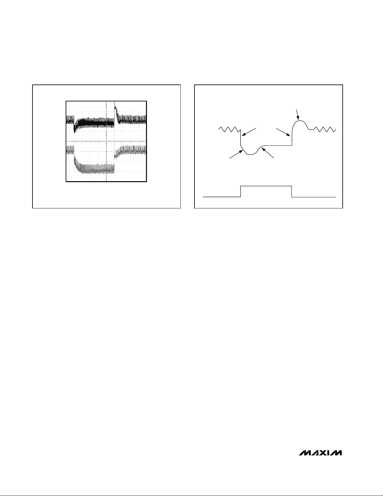
MAX1716/MAX1854/MAX1855
High-Speed, Adjustable, Synchronous Step-Down
Controllers with Integrated Voltage Positioning
26 ______________________________________________________________________________________
________________Applications Issues
Voltage Positioning and
Effective Efficiency
Powering new mobile processors requires careful
attention to detail to reduce cost, size, and power dissipation. As CPUs became more power hungry, it was
recognized that even the fastest DC-DC converters
were inadequate to handle the transient power requirements. After a load transient, the output instantly
changes by ESR
COUT
× ∆I
LOAD
. Conventional DC-DC
converters respond by regulating the output voltage
back to its nominal state after the load transient occurs
(Figure 7). However, the CPU only requires that the output voltage remain above a specified minimum value.
Dynamically positioning the output voltage to this lower
limit allows the use of fewer output capacitors and
reduces power consumption under load.
For a conventional (nonvoltage-positioned) circuit, the
total voltage change is:
V
P-P1
= 2 × (ESR
COUT
× ∆I
LOAD
) + V
SAG
+ V
SOAR
where V
SAG
and V
SOAR
are defined in Figure 8. Setting
the converter to regulate at a lower voltage when under
load allows a larger voltage step when the output current suddenly decreases (Figure 7). So the total voltage
change for a voltage positioned circuit is:
V
P-P2
= (ESR
COUT
× ∆I
LOAD
) + V
SAG
+ V
SOAR
where V
SAG
and V
SOAR
are defined in the Design
Procedure. Since the amplitudes are the same for both
circuits (V
P-P1
= V
P-P2
), the voltage-positioned circuit
requires only twice the ESR. Since the ESR specification is achieved by paralleling several capacitors, fewer
units are needed for the voltage-positioned circuit.
An additional benefit of voltage positioning is reduced
power consumption at high load currents. Because the
output voltage is lower under load, the CPU draws less
current. The result is lower power dissipation in the
CPU, although some extra power is dissipated in
R
SENSE
. For a nominal 1.6V, 18A output (R
LOAD
=
89mΩ), reducing the output voltage 2.9% gives an output voltage of 1.55V and an output current of 17.44A.
Given these values, CPU power consumption is
reduced from 28.8W to 27.03W. The additional power
consumption of R
SENSE
is:
2.5mΩ×(17.44A)2= 0.76W
and the overall power savings is as follows:
28.8W - (27.03W + 0.76W) = 1.01W
In effect, 1.8W of CPU dissipation is saved and the
power supply dissipates much of the savings, but both
the net savings and the transfer of heat away from the
CPU are beneficial. Effective efficiency is defined as
the efficiency required of a nonvoltage-positioned circuit to equal the total dissipation of a voltage-positioned circuit for a given CPU operating condition.
Calculate effective efficiency as follows:
1) Start with the efficiency data for the positioned
circuit (V
IN
, IIN, V
OUT
, I
OUT
).
2) Model the load resistance for each data point:
Figure 8. Transient-Response Regions
Figure 7. Voltage Positioning the Output
VOLTAGE POSITIONING THE OUTPUT
1.6V
1.6V
A. CONVENTIONAL CONVERTER (50mV/div)
B. VOLTAGE POSITIONED OUTPUT (50mV/div)
MAX1716-Figure 07
A
V
OUT
B
CAPACITIVE SAG
(dV/dt = I
I
LOAD
CAPACITOR SOAR
(ENERGY IN L
OUT/COUT
TRANSFERRED TO C
ESR STEP-DOWN
AND STEP-UP
X ESR)
(I
STEP
)
RECOVERY
OUT
)
Page 27

MAX1716/MAX1854/MAX1855
High-Speed, Adjustable, Synchronous Step-Down
Controllers with Integrated Voltage Positioning
______________________________________________________________________________________ 27
R
LOAD
= V
OUT
/ I
OUT
3) Calculate the output current that would exist for
each R
LOAD
data point in a nonpositioned
application:
INP= VNP/ R
LOAD
where VNP= 1.6V (in this example).
4) Calculate effective efficiency as:
Effective efficiency = (VNP× INP) / (VIN× IIN) =
calculated nonpositioned power output divided by
the measured voltage-positioned power input.
5) Plot the efficiency data point at the nonpositioned
current, I
NP
.
The effective efficiency of voltage-positioned circuits is
shown in the Typical Operating Characteristics.
Dropout Performance
The output-voltage adjustable range for continuousconduction operation is restricted by the nonadjustable
500ns (max) minimum off-time one-shot. For best
dropout performance, use the slower (200kHz) on-time
settings. When working with low input voltages, the
duty-factor limit must be calculated using worst-case
values for on- and off-times. Manufacturing tolerances
and internal propagation delays introduce an error to
the TON K-factor. This error is greater at higher frequencies (Table 3). Also, keep in mind that transient
response performance of buck regulators operated
close to dropout is poor, and bulk output capacitance
must often be added (see the V
SAG
equation in the
Design Procedure section).
The absolute point of dropout is when the inductor cur-
rent ramps down during the minimum off-time (∆I
DOWN
)
as much as it ramps up during the on-time (∆I
UP
). The
ratio h = ∆I
UP
/ ∆I
DOWN
is an indicator of ability to slew
the inductor current higher in response to increased
load and must always be >1. As h approaches 1, the
absolute minimum dropout point, the inductor current
cannot increase as much during each switching cycle,
and V
SAG
greatly increases unless additional output
capacitance is used.
A reasonable minimum value for h is 1.5, but adjusting
this up or down allows trade-offs between V
SAG
, output
capacitance, and minimum operating voltage. For a
given value of h, the minimum operating voltage can be
calculated as:
where V
DROP1
and V
DROP2
are the parasitic voltage
drops in the discharge and charge paths (see On-Time
One-Shot), t
OFF(MIN)
is from the Electrical
Characteristics table, and K is taken from Table 3. The
absolute minimum input voltage is calculated with h = 1.
If the calculated V
IN(MIN)
is greater than the required
minimum input voltage, then reduce the operating frequency or add output capacitance to obtain an acceptable V
SAG
. If operation near dropout is anticipated,
calculate V
SAG
to be sure of adequate transient re-
sponse.
Dropout Design Example:
V
OUT
= 1.6V
ƒ
SW
= 550kHz
K = 1.8µs, worst-case K = 1.58µs
t
OFF(MIN)
= 500ns
V
DROP1
= V
DROP2
= 100mV
h = 1.5
V
IN(MIN)
= [(1.6V + 0.1V) / (1 - (0.5µs × 1.5 / 1.58µs))] +
0.1V - 0.1V = 3.2V
Calculating again with h = 1 gives the absolute limit of
dropout:
V
IN(MIN)
= [(1.6V + 0.1V) / (1 - (0.5µs × 1.0 / 1.58µs))] +
0.1V - 0.1V = 2.5V
Therefore, VINmust be greater than 2.5V, even with
very large output capacitance, and a practical input
voltage with reasonable output capacitance would be
3.2V.
Adjusting V
OUT
with a Resistive Divider
The output voltage can be adjusted with a resistivedivider rather than the DAC if desired (Figure 9). The
drawback is that the on-time doesn’t automatically
receive correct compensation for changing output voltage levels. This can result in variable switching frequency as the resistor ratio is changed, and/or
excessive switching frequency. The equation for adjusting the output voltage is:
V
OUT
= VFB(1 + R1 / (R2 || R
INT
))
where V
FB
is the currently selected DAC value, and
R
INT
is the FB input resistance. In resistor-adjusted circuits, the DAC code should be set as close as possible
to the actual output voltage in order to minimize the
shift in switching frequency.
Adjusting V
OUT
Above 2V
The feed-forward circuit that makes the on-time dependent on the input voltage maintains a nearly constant
switching frequency as V+, I
LOAD
, and the DAC code
are changed. This works extremely well as long as FB
is connected directly to the output. When the output is
V
IN(MIN)
V
=
1 –
OUT
t
V
+
DROP1
OFF(MIN)
K
+ V
h
DROP2
– V
DROP1
Page 28

MAX1716/MAX1854/MAX1855
High-Speed, Adjustable, Synchronous Step-Down
Controllers with Integrated Voltage Positioning
28 ______________________________________________________________________________________
adjusted with a resistor-divider, the switching frequency is increased by the inverse of the divider ratio.
This change in frequency can be compensated with the
addition of a resistor-divider to the battery-sense input
(V+). Attach a resistor-divider from the battery voltage
to V+ on the MAX1716/MAX1854/MAX1855, with the
same attenuation factor as the output divider. The V+
input has a nominal input impedance of 600kΩ, which
should be considered when selecting resistor values.
One-Stage (Battery Input) vs. Two-Stage
(5V Input) Applications
The MAX1716/MAX1854/MAX1855 can be used with a
direct battery connection (one stage) or can obtain
power from a regulated 5V supply (two stage). Each
approach has advantages, and careful consideration
should go into the selection of the final design.
The one-stage approach offers smaller total inductor
size and fewer capacitors overall due to the reduced
demands on the 5V supply. The transient response of
the single stage is better due to the ability to ramp the
inductor current faster. The total efficiency of a single
stage is better than the two-stage approach.
The two-stage approach allows flexible placement due
to smaller circuit size and reduced local power dissipation. The power supply can be placed closer to the
CPU for better regulation and lower I
2
R losses from PC
board traces. Although the two-stage design has slow-
er transient response than the single stage, this can be
offset by the use of a voltage-positioned converter.
Ceramic Output Capacitor Applications
Ceramic capacitors have advantages and disadvantages. They have ultra-low ESR and are noncombustible, relatively small, and nonpolarized. However,
they are also expensive and brittle, and their ultra-low
ESR characteristic can result in excessively high ESR
zero frequencies. In addition, their relatively low capacitance value can cause output overshoot when stepping from full-load to no-load conditions, unless a small
inductor value is used (high switching frequency), or
there are some bulk tantalum or electrolytic capacitors
in parallel to absorb the stored inductor energy. In
some cases, there may be no room for electrolytics,
creating a need for a DC-DC design that uses nothing
but ceramics.
The MAX1716 can take full advantage of the small size
and low ESR of ceramic output capacitors in a voltagepositioned circuit. The addition of the positioning resistor increases the ripple at FB, lowering the effective
ESR zero frequency of the ceramic output capacitor.
Output overshoot (V
SOAR)
determines the minimum output capacitance requirement (see Output Capacitor
Selection). Often the switching frequency is increased
to 400kHz or 550kHz, and the inductor value is
reduced to minimize the energy transferred from inductor to capacitor during load-step recovery. The efficiency penalty for operating at 400kHz is about 2% to 3%
and about 5% at 550kHz when compared to the
300kHz voltage-positioned circuit, primarily due to the
high-side MOSFET switching losses.
Table 1 and the Typical Operating Characteristics
include a circuit using ceramic capacitors with a
550kHz switching frequency (Figure 13).
PC Board Layout Guidelines
Careful PC board layout is critical to achieve low
switching losses and clean, stable operation. The
switching power stage requires particular attention
(Figure 10). If possible, mount all of the power components on the top side of the board with their ground terminals flush against one another. Follow these
guidelines for good PC board layout:
1) Keep the high-current paths short, especially at the
ground terminals. This is essential for stable, jitterfree operation.
2) Connect all analog grounds to a separate solid cop-
per plane, which connects to the GND pin of the
MAX1716/MAX1854/MAX1855. This includes the
Figure 9. Adjusting V
OUT
with a Resistor-Divider
Q1
Q2
V
= VFB (1 + R4/R5)
OUT
R
SENSE
L1
V
OUT
R4
R5
MAX1716
MAX1854
MAX1855
DH
LX
DL
CS
VPS
PGND
FB
Page 29

MAX1716/MAX1854/MAX1855
High-Speed, Adjustable, Synchronous Step-Down
Controllers with Integrated Voltage Positioning
______________________________________________________________________________________ 29
VCC, REF, and CC capacitors, as well as the resistive-dividers connected to FB and ILIM.
3) Keep the power traces and load connections short.
This is essential for high efficiency. The use of thick
copper PC boards (2oz vs. 1oz) can enhance fullload efficiency by 1% or more. Correctly routing PC
board traces is a difficult task that must be
approached in terms of fractions of centimeters,
where a single mΩ of excess trace resistance causes a measurable efficiency penalty.
4) CS and PGND connections for current limiting must
be made using Kelvin sense connections to guarantee the current-limit accuracy.
5) When trade-offs in trace lengths must be made, it’s
preferable to allow the inductor charging path to be
made longer than the discharge path. For example,
it’s better to allow some extra distance between the
input capacitors and the high-side MOSFET than to
allow distance between the inductor and the low-side
MOSFET or between the inductor and the output filter
capacitor.
6) Ensure the FB connection to the output is short and
direct.
7) Route high-speed switching nodes away from sensitive analog areas (CC, REF, ILIM). Make all pin-strap
control input connections (SKIP, SHDN, ILIM, etc.) to
analog ground or VCCrather than PGND or VDD.
Layout Procedure
1) Place the power components first, with ground terminals adjacent (low-side MOSFET source, CIN, C
OUT
,
and D1 anode). If possible, make all these connections on the top layer with wide, copper-filled areas.
2)Mount the controller IC adjacent to the low-side
MOSFET. The DL gate trace must be short and wide,
measuring 10 to 20 squares (50mils to 100mils wide
if the MOSFET is 1 inch from the controller IC).
D1
Figure 10. Power-Stage PC Board Layout Example
SENSE
D1
D1
VIA TO V+
BATTERY
INPUT
C
IN
L1
GND
INPUT
GND
OUTPUT
C
OUT
V
OUT
VIA TO FB
ALL ANALOG GROUNDS
CONNECT TO LOCAL PLANE ONLY
MAX1717
V
CC
CC
REF
CONNECT LOCAL ANALOG GROUND PLANE DIRECTLY TO GND FROM
THE SIDE OPPOSITE THE V
CURRENTS FROM FLOWING IN THE ANALOG GROUND PLANE.
CAPACITOR GND TO AVOID VDD GROUND
DD
V
DD
VIA TO
GND
SOURCE
OF Q2
VIA TO CS
AND VPS
Q1
VIA TO GND
NEAR R
SENSE
R
Q2
VIA TO LX
NOTES: "STAR" GROUND IS USED.
D1 IS DIRECTLY ACROSS Q2.
INDUCTOR DISCHARGE PATH HAS LOW DC RESISTANCE.
Page 30
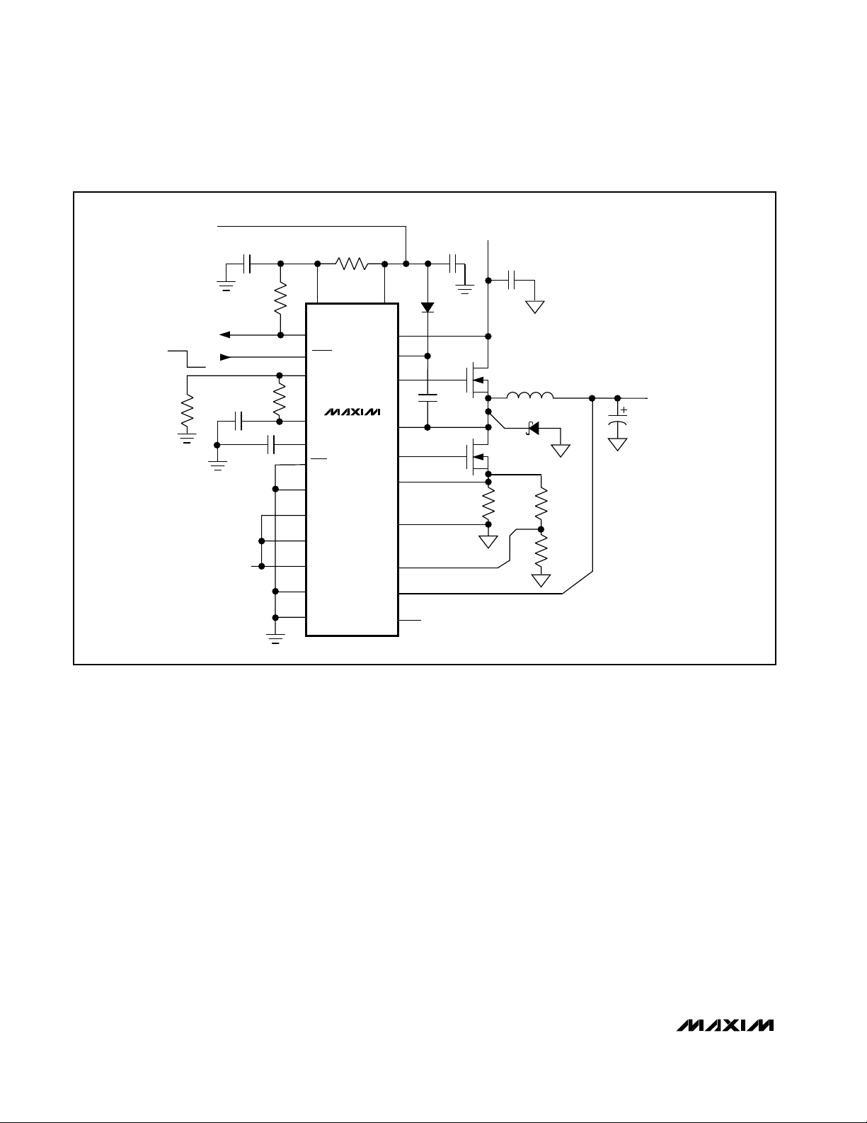
MAX1716/MAX1854/MAX1855
High-Speed, Adjustable, Synchronous Step-Down
Controllers with Integrated Voltage Positioning
30 ______________________________________________________________________________________
3) Group the gate-drive components (BST diode and
capacitor, VDDbypass capacitor) together near the
controller IC.
4) Make the DC-DC controller ground connections as
shown in Figure 1. This diagram can be viewed as
having three separate ground planes: output ground,
where all the high-power components go; the GND
plane, where the GND pin and VDDbypass capacitors go; and an analog ground plane where sensitive
analog components go. The analog ground plane
and GND plane must meet only at a single point
directly beneath the IC. These two planes are then
connected to the high-power output ground with a
short connection from GND to the source of the lowside MOSFET (the middle of the star ground). This
point must also be very close to the output capacitor
ground terminal.
5) Connect the output power planes (V
CORE
and system ground planes) directly to the output filter
capacitor positive and negative terminals with multiple vias. Place the entire DC-DC converter circuit as
close to the CPU as is practical.
___________________Chip Information
TRANSISTOR COUNT: 3729
Figure 11. Low-Current Application (Circuit #2)
+5V INPUT
BIAS SUPPLY
POWER-GOOD
INDICATOR
ON OFF
R6
100kΩ
MAX1716 DAC CODE SHOWN
C5
1µF
C1
0.22µF
TO V
100kΩ
300kΩ
CC
47pF
R3
10Ω
R4
MAX1716
MAX1854
MAX1855
V
DD
BST
DH
CS
PGND
VPS
TON
V+
LX
DL
FB
V
CC
VGATE
SHDN
ILIM
R5
REF
C2
CC
SKIP
D0
D1
D2
D3
D4
GND
C4
1µF
D1
C3
0.1µF
FLOAT (300kHz)
BATTERY (V
7V TO 24V
C
(4) 10µF
Q1
Q2
R
SENSE
3.5mΩ
IN
BATT
L1
1.0µH
D2
)
Q1: IRF7811
INTERNATIONAL RECTIFIER
Q2: (2) IRF7811
INTERNATIONAL RECTIFIER
D1: CMPSH-3
CENTRAL SEMICONDUCTOR
D2: CMSH2-60
CENTRAL SEMICONDUCTOR
1.3V OUTPUT
UP TO 12A
C
OUT
(4) 220µF
R1
1kΩ
R2
2kΩ
Page 31
MAX1716/MAX1854/MAX1855
High-Speed, Adjustable, Synchronous Step-Down
Controllers with Integrated Voltage Positioning
______________________________________________________________________________________ 31
Figure 12. Low-Voltage Application (Circuit #3)
+5V INPUT
BIAS SUPPLY
POWER-GOOD
INDICATOR
ON OFF
R6
100kΩ
MAX1716 DAC CODE SHOWN
C5
1µF
0.22µF
TO V
C1
CC
100kΩ
300kΩ
C2
47pF
BATTERY (V
7V TO 24V
R3
10Ω
R4
MAX1716
MAX1854
MAX1855
V
DD
BST
PGND
VPS
TON
V+
DH
LX
DL
CS
FB
V
CC
VGATE
SHDN
ILIM
R5
REF
CC
SKIP
D0
D1
D2
D3
D4
GND
C4
1µF
D1
C3
0.1µF
REF (400kHz)
Q1
Q2
R
3.5mΩ
C
IN
(4) 10µF
0.68µH
SENSE
L1
BATT
D2
)
R1
1kΩ
R2
2kΩ
Q1: IRF7811
INTERNATIONAL RECTIFIER
Q2: (2) IRF7811
INTERNATIONAL RECTIFIER
D1: CMPSH-3
CENTRAL SEMICONDUCTOR
D2: CMSH2-60
CENTRAL SEMICONDUCTOR
1.0V OUTPUT
UP TO 12A
C
OUT
(4) 220µF
Page 32

MAX1716/MAX1854/MAX1855
High-Speed, Adjustable, Synchronous Step-Down
Controllers with Integrated Voltage Positioning
32 ______________________________________________________________________________________
Figure 13. All-Ceramic-Capacitor Application (Circuit #4)
24
23
22
21
20
19
18
17
1
2
3
4
5
6
7
8
CS
LX
BST
SKIPFB
SHDN
V+
DH
TOP VIEW
D0
D1
D2
D3TON
V
CC
ILIM
CC
16
15
14
13
9
10
11
12
D4
V
DD
PGND
DLVGATE
VPS
GND
REF
QSOP
MAX1716
MAX1854
MAX1855
Pin Configuration
+5V INPUT
BIAS SUPPLY
POWER-GOOD
INDICATOR
ON OFF
R6
100kΩ
MAX1716 DAC CODE SHOWN
C5
1µF
0.22µF
TO V
C1
CC
100kΩ
200kΩ
C2
47pF
BATTERY (V
7V TO 24V
R3
10Ω
R4
MAX1716
MAX1854
MAX1855
V
DD
BST
PGND
VPS
TON
V+
DH
LX
DL
CS
FB
V
CC
VGATE
SHDN
ILIM
R5
REF
CC
SKIP
D0
D1
D2
D3
D4
GND
C4
1µF
D1
C3
0.1µF
GND (550kHz)
Q1
Q2
R
3mΩ
C
IN
(5) 10µF
0.47µH
SENSE
L1
BATT
D2
)
R2
1kΩ
R1
1kΩ
Q1: (2) IRF7811
INTERNATIONAL RECTIFIER
Q2: (2) IRF7811
INTERNATIONAL RECTIFIER
D1: CMPSH-3
CENTRAL SEMICONDUCTOR
D2: CMSH2-60
CENTRAL SEMICONDUCTOR
1.6V OUTPUT
UP TO 18A
C
OUT
(8) 47µF
Page 33

MAX1716/MAX1854/MAX1855
High-Speed, Adjustable, Synchronous Step-Down
Controllers with Integrated Voltage Positioning
Package Information
Maxim cannot assume responsibility for use of any circuitry other than circuitry entirely embodied in a Maxim product. No circuit patent licenses are
implied. Maxim reserves the right to change the circuitry and specifications without notice at any time.
33 ____________________Maxim Integrated Products, 120 San Gabriel Drive, Sunnyvale, CA 94086 408-737-7600
© 2000 Maxim Integrated Products Printed USA is a registered trademark of Maxim Integrated Products.
QSOP.EPS
 Loading...