

Page 1
General Description
The MAX1739/MAX1839 fully integrated controllers are
optimized to drive cold-cathode fluorescent lamps
(CCFLs) using the industry-proven Royer oscillator
inverter architecture. The Royer architecture provides
near sinusoidal drive waveforms over the entire input
range to maximize the life of CCFLs. The MAX1739/
MAX1839 optimize this architecture to work over a wide
input voltage range, achieve high efficiency, and maximize the dimming range.
The MAX1739/MAX1839 monitor and limit the transformer center-tap voltage when required. This ensures
minimal voltage stress on the transformer, which
increases the operating life of the transformer and
eases its design requirements. These controllers also
provide protection against many other fault conditions,
including lamp-out and buck short faults.
These controllers achieve 50:1 dimming range by
simultaneously adjusting lamp current and “chopping”
the CCFL on and off using a digitally adjusted pulsewidth modulated (DPWM) method. CCFL brightness is
controlled by an analog voltage or is set with an
SMBusTM-compatible two-wire interface (MAX1739).
The MAX1739/MAX1839 drive an external high-side
N-channel power MOSFET and two low-side N-channel
power MOSFETs, all synchronized to the Royer oscillator. An internal 5.3V linear regulator powers the MOSFET drivers and most of the internal circuitry. The
MAX1739/MAX1839 are available in space-saving
20-pin QSOP packages and operate over the -40°C to
+85°C temperature range.
________________________Applications
Notebook/Laptop Computers
Car Navigation Displays
LCD Monitors
Point-of-Sale Terminals
Portable Display Electronics
Features
♦ Fast Response to Input Change
♦ Wide Input Voltage Range (4.6V to 28V)
♦ High Power-to-Light Efficiency
♦ Minimizes Transformer Voltage Stress
♦ Lamp-Out Protection with 2s Timeout
♦ Buck Switch Short and Other Single-Point Fault
Protection
♦ Integrated Royer MOSFET Drivers Reduce
Transformer Pin Count
♦ Buck Operation Synchronized to Royer Oscillator
♦ Synchronizable DPWM Frequency
♦ Pin-Selectable Brightness Control Interface
♦ SMBus Serial Interface (MAX1739)
♦ Analog Interface (MAX1739/MAX1839)
MAX1739/MAX1839
†
Wide Brightness Range
CCFL Backlight Controllers
________________________________________________________________ Maxim Integrated Products 1
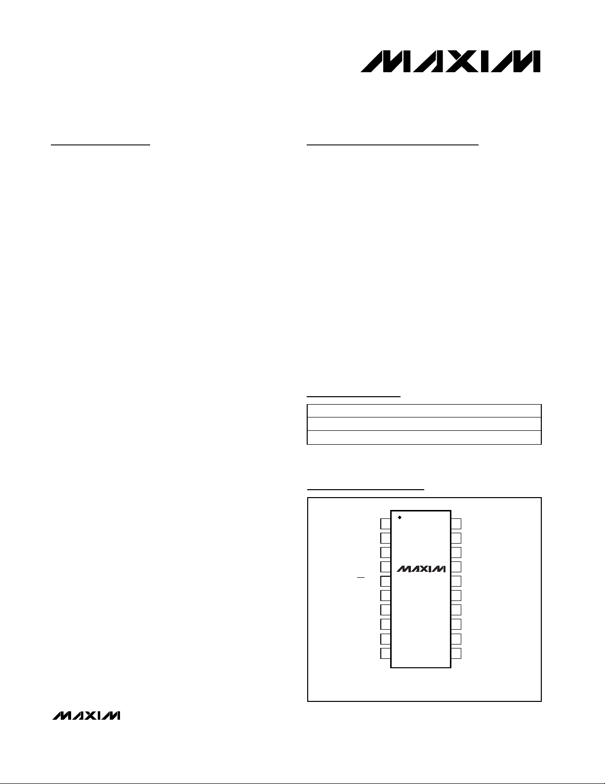
Pin Configuration
19-1755; Rev 1; 3/01
For price, delivery, and to place orders, please contact Maxim Distribution at 1-888-629-4642,
or visit Maxim’s website at www.maxim-ic.com.
†
Patent pending
SMBus is a trademark of Intel Corp.
Ordering Information
Pin Configurations continued at end of data sheet.
PART TEMP. RANGE PIN-PACKAGE
MAX1739EEP -40°C to +85°C 20 QSOP
MAX1839EEP -40°C to +85°C 20 QSOP
TOP VIEW
REF
MINDAC
CCI
SH/SUS
CRF/SDA
CTL/SCL
CSAV
1
2
3
4
MAX1739
5
6
7
8
9
10
20
BATT
19
DH
18
LX
17
BSTCCV
VL
16
GND
15
14
CS
DL1MODE
13
12
DL2
11
SYNCCTFB
QSOP
Page 2
MAX1739/MAX1839
†
Wide Brightness Range
CCFL Backlight Controllers
2 _______________________________________________________________________________________
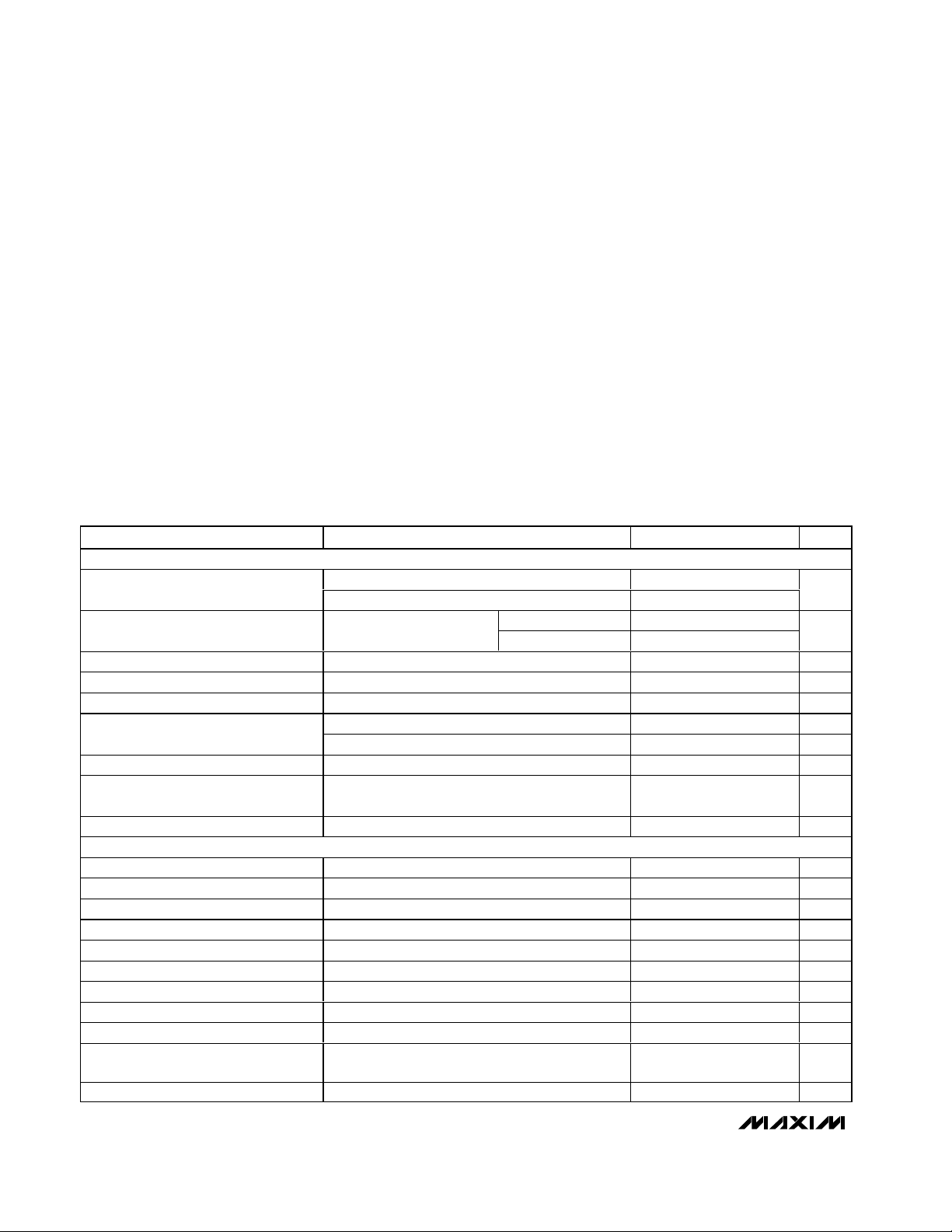
ABSOLUTE MAXIMUM RATINGS
ELECTRICAL CHARACTERISTICS
(V+ = 8.2V, VSH/SUS = VSH= 5.5V, MINDAC = GND, TA= 0°C to +85°C, unless otherwise noted. Typical values are at TA= +25°C.)
Stresses beyond those listed under “Absolute Maximum Ratings” may cause permanent damage to the device. These are stress ratings only, and functional
operation of the device at these or any other conditions beyond those indicated in the operational sections of the specifications is not implied. Exposure to
absolute maximum rating conditions for extended periods may affect device reliability.
VBATT to GND ...........................................................-0.3V to 30V
V
BST
, V
SYNC
to GND.................................................-0.3V to 34V
V
BST
to VLX.................................................................-0.3V to 6V
V
DH
to VLX.................................................-0.3V to (V
BST
+ 0.3V)
V
LX
to GND...................................................-6V to (V
BST
+ 0.3V)
VL to GND...................................................................-0.3V to 6V
V
CCV
, V
CCI
, V
REF
, V
DL1
, V
DL2
to GND .........-0.3V to (VL + 0.3V)
V
MINDAC
, V
CTFB
, V
CSAV
to GND ................................-0.3V to 6V
V
CS
to GND...................................................-0.6V to (VL + 0.3V)
V
MODE
to GND.............................................................-6V to 12V
V
CRF/SDA
, V
CRF
, V
CTL/SCL
, V
CTL
, V
SH/SUS
,
V
SH
to GND ............................................................-0.3V to 6V
Continuous Power Dissipation (T
A
= +70°C)
20-Pin QSOP (derate 9.1mW/°C above +70°C)...........727mW
Operating Temperature .......................................-40°C to +85°C
Storage Temperature.........................................-65°C to +150°C
Lead Temperature (soldering, 10s) .................................+300°C
SUPPLY AND REFERENCE
V
BATT
V
BATT
with Full Duty Cycle on DH
V
BATT
VL Output Voltage, Normal Operation
VL Output Voltage, Shutdown SH/SUS = SH = GND, no load 3.5 4.5 5.5 V
VL Undervoltage Lockout Threshold
VL Undervoltage Lockout Hysteresis 300 mV
REF Output Voltage, Normal
Operation
VL POR Threshold 0.9 2.7 V
SWITCHING REGULATOR
DH Driver On-Resistance 18 Ω
DL1, DL2 Driver On-Resistance 18 Ω
Minimum DH Switching Frequency 1/tDH, SYNC = CS or GND, not synchronized 49 56 64 kHz
DH Minimum Off-Time 250 375 500 ns
DH Maximum Duty Cycle 98 %
SYNC Synchronization Range Detect falling edges on SYNC 64 200 kHz
SYNC Input Current 0 < V
SYNC Input Threshold SYNC falling, referred to CS 400 500 600 mV
SYNC Input Hysteresis Referred to the SYNC input threshold 50 100 150 mV
SYNC Threshold Crossing to DL1,
DL2 Toggle Delay
CS Overcurrent Threshold 408 450 492 mV
PARAMETER CONDITIONS MIN TYP MAX UNITS
VL = V
Input Voltage Range
Quiescent Current, Operation
BATT
V
= open 6 28
L
DH = DL1 = DL2 = open
Quiescent Current, Shutdown SH/SUS = SH = GND 6 20 µA
6V < V
< 28V, 0 < I
BATT
VL rising (leaving lockout) 4.6
VL falling (entering lockout) 4.0 V
4.5V < VL < 5.5V, I
< 30V -2 2 µA
SYNC
V
= 0 to 5V, C
SYNC
50% point on SYNC to 50% point on DL1 or DL2
4.6 5.5
V
= 28V 3.2 6
BATT
= VL = 5V 3.2 6
V
BATT
< 15mA
LOAD
= 40µA 1.96 2.00 2.04 V
REF
DL_1
and C
DL_2
< 100pF,
5.0 5.35 5.5 V
120 ns
V
mA
Page 3

MAX1739/MAX1839
†
Wide Brightness Range
CCFL Backlight Controllers
_______________________________________________________________________________________ 3
ELECTRICAL CHARACTERISTICS (continued)
(V+ = 8.2V, VSH/SUS = VSH= 5.5V, MINDAC = GND, TA= 0°C to +85°C, unless otherwise noted. Typical values are at TA= +25°C.)
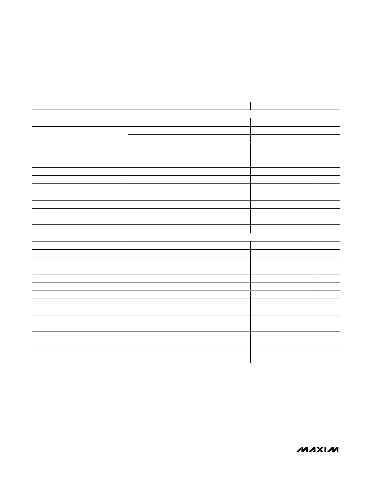
DAC AND ERROR AMPLIFIER
DAC Resolution Guaranteed monotonic 5 Bits
MINDAC Input Voltage Range 0 2 V
MINDAC Input Bias Current 0 < V
MINDAC Digital PWM Disable
Threshold
CSAV Input Voltage Range 0 0.8 V
CSAV Regulation Point
CSAV Input Bias Current -1 1 µA
CSAV to CCI Transconductance 1V < V
CTFB Input Voltage Range 0 2 V
CTFB Input Bias Current -1 1 µA
CTFB Regulation Point 570 600 630 mV
CTFB to CCV Transconductance 1V < V
TIMERS AND FAULT DETECTION
Chopping Oscillator Frequency No AC signal on MODE, not synchronized 24 28 32 kHz
Digital PWM Chop-Mode Frequency
MODE to DPWM Sync Ratio F
Lamp-Out Detection Timeout Timer
(Center-Tap Voltage Stuck at
Maximum) (Note 1)
CSAV Lamp-Out Threshold 50 75 100 mV
Fault-Detection Threshold on CCV (Note 2) 0.4 1 V
Shorted Buck-Switch Detection
Timeout Timer (UL1950 Protection)
(Note 3)
Lamp Turn-On Delay After SH/SUS or SH forces device on or SH rises 4 ms
MODE Operating Voltage Range -5.5 11 V
MODE = GND Threshold
(min Brightness = 0)
MODE = REF Threshold
(max Brightness = 0)
MODE = VL Threshold
(MAX1739 SMB Interface Mode)
MODE AC Signal Amplitude Peak to peak (Note 5) 2 V
MODE AC Signal Synchronization
Range
PARAMETER CONDITIONS MIN TYP MAX UNITS
< 2V -1 1 µA
MINDAC
MINDAC = VL 2.4 2.9 4 V
V
V
V
No AC signal on MODE 205 220 235
32kHz AC signal on MODE 250
100kHz AC signal on MODE 781
V
lamp-out
threshold
V
detection
threshold on CCV
To sync DPWM oscillator, not in shutdown
(Note 4)
To sync DPWM oscillator, not in shutdown
(Note 4)
To sync DPWM oscillator, not in shutdown
(Note 4)
Chopping oscillator synchronized to MODE AC
signal
= 0, DAC code = 11111 binary 188 194 200
MINDAC
= 0, DAC code = 00001 binary 2 6.25 16
MINDAC
= 1V, DAC code = 00000 binary 93 100 110
MINDAC
< 2.7V 100 µmho
CCI
< 2.7V 30 40 50 µmho
CCV
/ F
MODE
CSAV
CCV
DPWM
< CSAV
< fault-
No AC signal on MODE 2.06 2.33 2.73
32kHz AC signal on MODE 2.05
100kHz AC signal on MODE 0.66
No AC signal on MODE 332 291 259
32kHz AC signal on MODE 256
100kHz AC signal on MODE 82
1.4 2.6 V
VL - 0.6 V
32 100 kHz
mV
Hz
128
s
ms
0.6 V
Page 4
MAX1739/MAX1839
†
Wide Brightness Range
CCFL Backlight Controllers
4 _______________________________________________________________________________________
ELECTRICAL CHARACTERISTICS (continued)
(V+ = 8.2V, VSH/SUS = VSH= 5.5V, MINDAC = GND, TA= 0°C to +85°C, unless otherwise noted. Typical values are at TA= +25°C.)
ANALOG INTERFACE BRIGHTNESS CONTROL (MODE connected to REF or GND )
CRF/SDA, CRF Input Range 2.7 5.5 V
CRF/SDA, CRF Input Current
CTL/SCL, Input Range MAX1739 0
CTL Input Range MAX1839 0 CRF V
CTL/SCL, CTL Input Current MODE = REF or GND -1 1 µA
ADC Resolution Guaranteed monotonic 5 Bits
ADC Hysteresis 1 LSB
SH Input Low Voltage 0.8 V
SH Input High Voltage 2.1 V
SH/SUS Input Hysteresis when
Transitioning In and Out of Shutdown
SH Input Bias Current -1 1 µA
SYSTEM MANAGEMENT BUS BRIGHTNESS CONTROL (MAX1739, MODE connected to VL, see Figures 12 and 13)
CRF/SDA, CTL/SCL, SH/SUS Input
CRF/SDA, CTL/SCL, SH/SUS Input
CRFSDA, CTLSCL Input Hysteresis 300 mV
CRF/SDA, CTL/SCL, SH/SUS Input
CRF/SDA Output Low Sink Current V
CTL/SCL Serial Clock High Period t
CTL/SCL Serial Clock Low Period t
Start Condition Setup Time t
Start Condition Hold Time t
C RF/S D A V al id to C TL/S C L Ri si ng E d g e
S etup Ti m e, S l ave C l ocki ng i n D ata
CTL/SCL Falling Edge to CRF/SDA
Transition
CTL/SCL Falling Edge to CRF/SDA
Valid, Reading Out Data
PARAMETER CONDITIONS MIN TYP MAX UNIT
= V
V
CRF/SDA
V
CRF/SDA
CRF/SDA
HIGH
LOW
SU:STA
HD:STA
t
SU:DAT
t
HD:DAT
t
DV
= 0.4V 4 mA
= 5.5V 20 µA
CRF
= V
= 5.5V, SH/SUS = SH = 0 -1 1 µA
CRF
150 mV
2.1 V
-1 1 µA
4µs
4.7 µs
4.7 µs
4µs
250 ns
0ns
CRF/
SDA
0.8 V
1µs
V
Page 5
MAX1739/MAX1839
†
Wide Brightness Range
CCFL Backlight Controllers
_______________________________________________________________________________________ 5
ELECTRICAL CHARACTERISTICS
(V+ = 8.2V, VSH/SUS = VSH= 5.5V, MINDAC = GND, TA= -40°C to +85°C, unless otherwise noted.) (Note 6)
Note 1: Corresponds to 512 DPWM cycles or 65536 MODE
cycles.
Note 2: When the buck switch is shorted, V
CTFB
goes high
causing V
CCV
to go below the fault detection threshold.
Note 3: Corresponds to 64 DPWM cycles or 8192 MODE cycles.
Note 4: The MODE pin thresholds are only valid while the part is
operating. In shutdown, V
REF
= 0 and the part only
differentiates between SMB mode and ADC mode. In
shutdown with ADC mode selected, the CRF/SDA and
CTL/SCL pins are at high impedance and will not cause
extra supply current when their voltages are not at
GND or VL.
V
AMPLITUDE
> 2V
MODE
500pF
10k
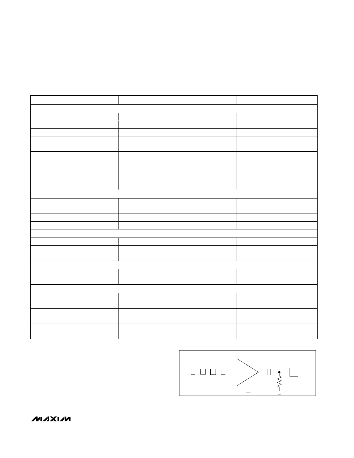
Note 5: The amplitude is measured with the following circuit:
Note 6: Specifications from -40°C to +85°C are guaranteed by
design, not production tested.
SUPPLY AND REFERENCE
V
BATT
V
BATT
VL Output Voltage, Normal Operation
VL Undervoltage Lockout Threshold
REF Output Voltage, Normal
Operation
VL POR Threshold 0.9 2.7 V
SWITCHING REGULATOR
DH Driver On-Resistance 18 Ω
DL1, DL2 Driver On-Resistance 18 Ω
SYNC Synchronization Range Detect falling edges on SYNC 64 200 kHz
CS Overcurrent Threshold 408 492 mV
DAC AND ERROR AMPLIFIER
CSAV Regulation Point V
CTFB Regulation Point 560 640 mV
CTFB to CCV Transconductance 1V < V
ANALOG INTERFACE BRIGHTNESS CONTROL (MODE connected to REF or MODE connected to GND)
SH Input Low Voltage 0.8 V
SH Input High Voltage 2.1 V
SYSTEM MANAGEMENT BUS BRIGHTNESS CONTROL (MODE connected to VL)
CRF/SDA, CTL/SCL, SH/SUS Input
Low Voltage
CRF/SDA, CTL/SCL, SH/SUS Input
High Voltage
PARAMETER CONDITIONS MIN TYP MAX UNITS
VL = V
Input Voltage Range
Quiescent Current, Shutdown SH/SUS = SH = GND 20 µA
BATT
VL = open 6 28
6V < V
0 < I
VL rising (leaving lockout) 4.6
VL falling (entering lockout) 4.0
4.5V < VL < 5.5V, I
MINDAC
< 28V,
BATT
< 15mA
LOAD
= 40µA 1.95 2.05 V
REF
= 0, DAC code = 11111 binary 186 202 mV
< 2.7V 30 50 µmho
CCV
4.6 5.5
5.0 5.6 V
0.8 V
2.1 V
V
V
CRF/SDA Output Low Sink Current V
CRF/SDA
= 0.4V 4 mA
Page 6
MAX1739/MAX1839
†
Wide Brightness Range
CCFL Backlight Controllers
6 _______________________________________________________________________________________
Typical Operating Characteristics
(VIN= 12V, V
CTL
= V
CRF
, V
MINDAC
= 1V, MODE = GND, Circuit of Figure 8.)
4µs/div
WIDE INPUT RANGE
(V
BATT
= 8V)
V
CSAV
500mV/div
V
CTAP
5V/div
V
DH
20V/div
MAX1739/1839 toc01
4µs/div
WIDE INPUT RANGE
(V
BATT
= 20V)
V
CSAV
500mV/div
V
CTAP
5V/div
V
DH
20V/div
MAX1739/1839 toc02
100µs/div
V
CCI
V
CCI
V
CCI
V
CCV
V
CCV
V
CCV
WIDE INPUT RANGE
(V
BATT
= 8V, DPWM = 9%, V
CTL
= 0)
V
CSAV
500mV/div
V
CTAP
10V/div
V
CCV, VCCI
200mV/div
1.2V
MAX1739/1839 toc03
100µs/div
V
CCI
V
CCI
V
CCI
V
CCV
V
CCV
V
CCV
WIDE INPUT RANGE
(V
BATT
= 20V, DPWM = 9%, V
CTL
= 0)
V
CSAV
500mV/div
V
CTAP
10V/div
V
CCV, VCCI
200mV/div
1.2V
MAX1739/1839 toc04
20µs/div
FEED-FORWARD COMPENSATION
V
CTAP
5mV/div
V
IN
20V
10V
V
CSAV
500mV/div
V
DH
20V/div
MAX1739/1839 toc05
4µs/div
SWITCHING WAVEFORMS
V
CSAV
500mV/div
V
CTAP
10V/div
V
DH
20V/div
V
DL
5V/div
MAX1739/1839 toc08
Page 7

MAX1739/MAX1839
†
Wide Brightness Range
CCFL Backlight Controllers
_______________________________________________________________________________________ 7
Typical Operating Characteristics (continued)
(VIN= 12V, V
CTL
= V
CRF
, V
MINDAC
= 1V, MODE = GND, Circuit of Figure 8.)
20ms/div
STARTUP
(ADC SOFT-START, MODE = GND)
V
CTAP
10V/div
V
BATT
V
CSAV
500mV/div
I
BATT
500mA/div
MAX1739/1839 toc09
12V
0
2ms/div
LAMP-OUT VOLTAGE LIMITING
V
SECONDARY
2kV/div
V
CTAP
5V/div
MAX1739/1839 toc10
1ms/div
SYNCHRONIZED DPWM
(f
MODE
= 100kHz, V
CTL
= V
CRF
/2)
V
CSAV
500mV/div
V
CTAP
5V/div
V
DH
20V/div
MAX1739/1839 toc07
1ms/div
SYNCHRONIZED DPWM
(f
MODE
= 32kHz, V
CTL
= V
CRF
/2)
V
CSAV
500mV/div
V
CTAP
5V/div
V
DH
20V/div
MAX1739/1839 toc06
400ms/div
LAMP-OUT VOLTAGE LIMITING
V
SECONDARY
2kV/div
V
CTAP
5V/div
MAX1739/1839 toc11
0
200
100
500
400
300
800
700
600
900
0105 152025
INPUT CURRENT vs.
INPUT VOLTAGE
MAX1739/1839 toc12
V
BATT
(V)
I
BATT
(mA)
0
2
1
5
4
3
8
7
6
9
SHUTDOWN CURRENT (µA)
SHUTDOWN
MINIMUM BRIGHTNESS
MAXIMUM BRIGHTNESS
Page 8
MAX1739/MAX1839
†
Wide Brightness Range
CCFL Backlight Controllers
8 _______________________________________________________________________________________
Typical Operating Characteristics (continued)
(VIN= 12V, V
CTL
= V
CRF
, V
MINDAC
= 1V, MODE = GND, Circuit of Figure 8.)
5.40
5.35
5.30
5.25
VL (V)
5.20
5.15
5.10
NORMAL OPERATION
SHUTDOWN
0.01 1 100.1 100
VL vs. I
VL
IVL (mA)
MAX1739/1839 toc13
5.36
5.35
5.34
VL (V)
5.33
VL vs. BATT VOLTAGE
NORMAL OPERATION
SHUTDOWN
0101552520
V
(V)
BATT
4.60
4.55
4.50
4.45
SHUTDOWN VL (V)
MAX1739/1839 toc14
4.6
4.5
4.4
4.3
SHUTDOWN VL (V)
4.2
4.1
4.0
VL vs. TEMPERATURE
SHUTDOWN
NORMAL OPERATION
VL (V)
MAX1739/1839 toc15
6
5
4
3
2
1
0
5.32
5.31
-40 10-15 356085
TEMPERATURE (°C)
4.40
4.35
Page 9

MAX1739/MAX1839
†
Wide Brightness Range
CCFL Backlight Controllers
_______________________________________________________________________________________ 9_______________________________________________________________________________________
Pin Description
PIN
1 REF REF 2V Reference Output. Bypass to GND with 0.1µF. Forced low during shutdown.
2 MINDAC MINDAC
3 CCI CCI
4 CCV CCV
5 SH/SUS SH
6 CRF/SDA CRF
7 CTL/SCL CTL
8 MODE MODE
9 CSAV CSAV Current-Sense Input. Input to the GMI error amplifier that drives CCI.
10 CTFB CTFB Center-Tap Voltage Feedback Input. The average V
11 SYNC SYNC
12 DL2 DL2
13 DL1 DL1 Low-Side N-Channel MOSFET 1 Gate Drive
14 CS CS
15 GND GND System Ground
16 VL VL
17 BST BST
18 LX LX High-Side Driver Ground Input
19 DH DH High-Side Gate Driver Output. Falling edges on SYNC turn on DH.
20 BATT BATT Supply Input. Input to the internal 5.3V linear regulator that powers the chip.
MAX1739 MAX1839
NAME
DAC Zero-Scale Input. V
Disable DPWM by connecting MINDAC to VL.
GMI Output. Output of the current loop GMI amplifier that regulates the CCFL current.
Typically bypass to GND with 0.1µ F .
GMV Output. Output of the voltage loop GMV amplifier that regulates the maximum
average primary transformer voltage. Typically bypass to GND with 3300p F .
Logic Low Shutdown Input in Analog Interface Mode. SMBus suspends input in SMBus
interface mode (MAX1739 only).
5- Bi t AD C Reference Input in Anal og Inter face Mod e. Bypass to GN D wi th 0.1µF. SM Bus seri al
d ata i np ut/op en- d r ai n outp ut ( MAX 1739 onl y) i n S M Bus i nter face m od e.
CCFL Brightness Control Input in Analog Interface Mode. SMBus serial clock input
(MAX1739 only) in SMBus interface mode.
Interface Selection Input and Sync Input for DPWM Chopping (see Synchronizing the
DPWM Frequency). The average voltage on the MODE pin selects one of three CCFL
brightness control interfaces:
1) MODE = VL, enables SMBus serial interface (MAX1739 only).
2) MODE = GND, enables the analog interface (positive scale analog interface mode);
V
CTL/SCL
3) MODE = REF, enables the analog interface (negative scale analog interface mode);
V
CTL/SCL
Royer Synchronization Input. Falling edges on SYNC force DH on and toggle the DL1
and DL2 drivers. Connect directly to the Royer center tap.
Low-Side N-Channel MOSFET 2 Gate Drive. Drives the Royer oscillator switch. DL1 and
DL2 have make-before-break switching, where at least one is always on. Falling edges
on SYNC toggle DL1 and DL2 and turn DH on.
Current-Sense Input (Current Limit). The current-mode regulator terminates the switch
cycle when VCS exceeds (V
5.3V Linear Regulator Output. Supply voltage for most of the internal circuits. Bypass
with 1µF capacitor to GND. Can be connected to V
High-Side Driver Bootstrap Input. Connect through a diode to VL and bypass with 0.1µF
capacitor to LX.
= 0 means minimum brightness.
= 0 means maximum brightness.
MINDAC
REF
FUNCTION
sets the DAC’s minimum scale output voltage.
CTFB
- V
).
CCI
BATT
is limited to 0.6V.
if V
BATT
< 5.5V.
Page 10

MAX1739/MAX1839
†
Wide Brightness Range
CCFL Backlight Controllers
10 ______________________________________________________________________________________
Detailed Description
The MAX1739/MAX1839 regulate the brightness of a
CCFL in three ways:
1) Linearly controlling the lamp current.
2) Digitally pulse-width modulating (or chopping) the
lamp current (DPWM).
3) Using both methods simultaneously for widest dimming range.
DPWM is implemented by pulse-width modulating the
lamp current at a rate faster than the human eye can
detect. Figure 1 shows the current and voltage waveforms for the three operating modes with the brightness
control set to 50% of full scale.
The MAX1739/MAX1839 include a 5.3V linear regulator
to power most of the internal circuitry, drivers for the
buck and Royer switches, and the synchronizable
DPWM oscillator. The MAX1739/MAX1839 are very flexible and include a variety of operating modes, an analog interface, an SMBus interface (MAX1739 only), a
shutdown mode, lamp-out detection, and buck-switch
short detection.
Figure 1. Brightness Control Methods
V
= 0
MINDAC
= V
V
CTL
(DAC SET TO MIDSCALE)
EFFECTIVE BRIGHTNESS IS:
50% IN CONTINUOUS AND DPWM CONTROL
25% IN COMBINED CONTROL
/2 or BRIGHT[4:0] = 10,000
CRF
DPWM CONTROL
V
CTAP
TRANSFORMER
VOLTAGE
V
CSAV
LAMP CURRENT
CONTINUOUS CURRENT CONTROL
V
CTAP
V
CSAV
CURRENT + DPWM CONTROL
Page 11

MAX1739/MAX1839
†
Wide Brightness Range
CCFL Backlight Controllers
_______________________________________________________________________________________ 11
Voltage and Current Control Loops
The MAX1739/MAX1839 use two control loops. The current control loop regulates the average lamp current. The
voltage control loop limits the maximum average primaryside transformer voltage. The voltage control loop is
active during the beginning of DPWM on-cycles and in
some fault conditions. Limiting the transformer primary
voltage allows for a lower transformer secondary voltage
rating that can increase reliability and decrease cost of
the transformer. The voltage control loop acts to limit the
transformer voltage any time the current control loop
attempts to steer the transformer voltage above its limit as
set by V
CTFB
(see Sense Resistors).
The voltage control loop uses a transconductance
amplifier to create an error current based on the voltage between CTFB and the internal reference level
(600mV typ) (Figure 2). The error current is then used
to charge and discharge C
CCV
to create an error volt-
age V
CCV
. The current control loop produces a similar
signal based on the voltage between CSAV and its
internal reference level (see the Dimming Range section). This error voltage is called V
CCI
. The lower of
V
CCV
and V
CCI
is used with the buck regulator’s PWM
ramp generator to set the buck regulator’s duty cycle.
During DPWM, the two control loops work together to
limit the transformer voltage and to allow wide dimming
range with good line rejection. During the DPWM offcycle, V
CCV
is set to 1.2V and CCI is set to high imped-
ance. V
CCV
is set to 1.2V to create soft-start at the
beginning of each DPWM on-cycle in order to avoid
overshoot on the transformer primary. V
CCI
is set to
high impedance to keep V
CCI
from changing during the
off-cycles. This allows the current control loop to regulate the average lamp current only during DPWM oncycles and not the overall average lamp current.
Upon power-up, V
CCI
slowly rises, increasing the duty
cycle, which provides soft-start. During this time, V
CCV
,
which is the faster control loop, is limited to 150mV
above V
CCI
by the CCV-CLAMP
. Once the secondary
voltage reaches the strike voltage, the lamp current
begins to increase. When the lamp current reaches the
regulation point, V
CCI
reaches steady state. With MINDAC = VL (DPWM disabled), the current control loop
remains in control and regulates the lamp current.
With MINDAC between REF and GND, DPWM is
enabled and the MAX1739/MAX1839 begin pulsing the
lamp current. During the on-cycle, V
CCV
is at 150mV
above V
CCI
. After the on-cycle, V
CCV
is forced down to
1.2V to provide soft-start at the beginning of the next
on-cycle. Also, V
CCI
retains its value until the beginning
of the next on-cycle. When V
CCV
increases, it causes
the buck regulator duty cycle to increase and provides
soft-start. When V
CCV
crosses over V
CCI
, the current
control loop regains control and regulates the lamp current. V
CCV
is limited to 150mV above V
CCI
for the
remainder of the on-cycle.
In a lamp-out condition, V
CCI
increases the primary
voltage in an attempt to maintain lamp current regulation. As V
CCI
rises, V
CCV
rises with it until the primary
voltage reaches its set limit point. At this point, V
CCV
stops rising and limits the primary voltage by limiting
the duty cycle. Because V
CCV
is limited to 150mV
above V
CCI
, the voltage control loop is quickly able to
limit the primary voltage. Without this clamping feature,
the transformer voltage would overshoot to dangerous
levels because V
CCV
would take more time to slew
down from its supply rail. Once the MAX1739/MAX1839
sense less than 1/6 the full-scale current through the
lamp for 2 seconds, it shuts down the Royer oscillator
(see Lamp-Out Detection).
See the Sense Resistors section for information about
setting the voltage and current control loop thresholds.
Feed-Forward Control
Both control loops are influenced by the input voltage
feed-forward (V
BATT
) control circuitry of the MAX1739/
MAX1839. Feed-forward control instantly adjusts the
buck regulator’s duty cycle when it detects a change in
input voltage. This provides immunity to changes in
input voltage at all brightness levels. This feature
makes compensation over wide input ranges easier,
makes startup transients less dependent on input voltage, and improves line regulation for short DPWM ontimes.
The MAX1739/MAX1839 feed-forward control is implemented by varying the amplitude of the buck-switch’s
PWM ramp amplitude. This has the effect of varying the
duty cycle as a function of input voltage while maintaining the same V
CCI
and V
CCV
. In other words, V
BATT
feed
forward has the effect of not requiring changes in errorsignal voltage (V
CCI
and V
CCV
) to respond to changes in
V
BATT
. Since the capacitors only need to change their
voltage minimally to respond to changes in V
BATT
, the
controller’s response is essentially instantaneous.
Transient Overvoltage Protection
from Dropout
The MAX1739/MAX1839 are designed to maintain tight
control of the transformer primary under all transient
conditions. This includes transients from dropout,
where V
BATT
is so low that the controller loses regulation and reaches maximum duty cycle. Backlight
designs will want to choose circuit component values to
minimize the transformer turns ratio in order to minimize
primary-side currents and I2R losses. To achieve this,
Page 12

MAX1739/MAX1839
†
Wide Brightness Range
CCFL Backlight Controllers
12 ______________________________________________________________________________________
Figure 2. Functional Diagram
REF
MINDAC
DPWM CONTROL
LAMP CURRENT AND
SMBus
CTL/SCL
CRF/SDA
VL
GND
DPWM OSC
MODE
BATT
REF
VL
PEAK
DETECTOR
VL
SUPPLY
GMI
SH/SUS
MINDAC = VL?
PWM
PK_DET_CLAMP
CCI
CSAV
REF
Y = 1, N = 0
RAMP
GENERATOR
CCV CLAMP
CCV
BUCK
0.6V
BST
ENABLE
BUCK REGULATOR
GMV
CTFB
LX
DH
PWM CONTROL
450mV
CS
500mV
DL1
CS
ROYER OSC
SYNC
DL2
CS
Page 13

MAX1739/MAX1839
†
Wide Brightness Range
CCFL Backlight Controllers
______________________________________________________________________________________ 13
allow the circuit to operate in dropout at extremely low
battery voltages where the backlight’s performance is
secondary. All backlight circuit designs can undergo a
transient overvoltage condition when the laptop is
plugged into the AC adapter and V
BATT
suddenly
increases. The MAX1739/MAX1839 contain a unique
clamp circuit on V
CCI
. Along with the feed-forward circuitry, it ensures that there is not a transient transformer
overvoltage when leaving dropout.
The PK_DET_CLAMP circuit limits V
CCI
to the peaks of
the buck-regulator’s PWM ramp generator. As the circuit reaches dropout, V
CCI
approaches the peaks of
the PWM ramp generator in order to reach maximum
duty cycle. If V
BATT
decreases further, the control loop
loses regulation and V
CCI
tries to reach its positive sup-
ply rail. The clamp circuit on V
CCI
keeps this from hap-
pening, and V
CCI
rides just above the peaks of the
PWM ramp. As V
BATT
decreases further, the feed-forward PWM ramp generator loses amplitude and the
clamp drags V
CCI
down with it to a voltage below
where V
CCI
would have been if the circuit was not in
dropout. When VBATT is suddenly increased out of
dropout, V
CCI
is still low and maintains the drive on the
transformer at the old dropout level. The circuit then
slowly corrects and increases V
CCI
to bring the circuit
back into regulation.
Buck Regulator
The buck regulator uses the signals from the PWM
comparator, the current-limit detection on CS, and
DPWM signals to control the high-side MOSFET duty
cycle. The regulator uses voltage-mode PWM control
and is synchronized to the Royer oscillator. A falling
edge on SYNC turns on the high-side MOSFET after a
375ns minimum off-time delay. The PWM comparator or
the CS current limit ends the on-cycle.
Interface Selection
Table 1 lists the functionality of SH/SUS, CRF/SDA, and
CTL/SCL in each of the three interface modes of the
MAX1739/MAX1839. The MAX1739 features both an
SMBus digital interface and an analog interface, while
the MAX1839 features only the analog interface. Note
that MODE can also synchronize the DPWM frequency
(see Synchronizing the DPWM Frequency).
Dimming Range
Brightness is controlled by either the analog interface
(see Analog Interface) or the SMBus interface (see
SMBus Interface). CCFL brightness is adjusted in three
ways:
1) Lamp current control, where the magnitude of the
average lamp current is adjusted.
2) DPWM control, where the average lamp current is
pulsed to the lamp with a variable duty cycle.
3) A combination of the first two methods.
In each of the three methods, a 5-bit brightness code is
generated from the selected interface and is used to
set the lamp current and/or DPWM duty cycle.
The 5-bit brightness code defines the lamp current
level with ob00000 representing minimum lamp current
and ob11111 representing maximum lamp current. The
average lamp current is measured across an external
sense resistor (see Sense Resistors). The voltage on
the sense resistor is measured at CSAV. The brightness
code adjusts the regulation voltage at CSAV (V
CSAV
).
The minimum average V
CSAV
is V
MINDAC
/10, and the
maximum average is set by the following formula:
V
CSAV
= V
REF
✕
31 / 320 + V
MINDAC
/ 320
which is between 193.75mV and 200mV.
Note that if V
CSAV
does not exceed 100mV peak (which
is about 32mV average) for over 2 seconds, the
MAX1739/MAX1839 will assume a lamp-out condition
and shut down (see Lamp-Out Detection).
The equation relating brightness code to C
SAV
regula-
tion voltage is:
V
CSAV
= V
REF
✕
n / 320 + V
MINDAC
✕
(32 - n) / 320
where n is the brightness code.
To always use maximum average lamp current when
using DPWM control, set V
MINDAC
to V
REF
.
DPWM control works similar to lamp current control in
that it also responds to the 5-bit brightness code. A
Table 1. Interface Modes
PIN
SH/SUS SMBus suspend Logic-level shutdown control input
CRF/SDA SMBus data I/O Reference input for minimum brightness Reference input for maximum brightness
CTL/SCL SMBus clock input Analog control input to set brightness (range from 0 to CRF/SDA)
DIGITAL
INTERFACE
MODE = VL
(MAX1739 only)
MODE = REF,
/SCL = 0 = maximum brightness
V
CTL
ANALOG INTERFACE
MODE = GND,
V
/SCL = 0 = minimum brightness
CTL
Page 14

MAX1739/MAX1839
†
Wide Brightness Range
CCFL Backlight Controllers
14 ______________________________________________________________________________________
brightness code of ob00000 corresponds to a 9.375%
DPWM duty cycle, and a brightness code of ob11111
corresponds to a 100% DPWM duty cycle. The duty
cycle changes by 3.125% per step, except codes
ob00000 to ob00011 all produce 9.375% (Figure 3).
To disable DPWM and always use 100% duty cycle, set
V
MINDAC
to VL. Note that with DPWM disabled, the
equations above should assume V
MINDAC
= 0 instead
of V
MINDAC
= VL. Table 2 lists MINDAC’s functionality,
and Table 3 shows some typical settings for the brightness adjustment.
In normal operation, V
MINDAC
is set between 0 and
V
REF
, and the MAX1739/MAX1839 use both lamp current control and DPWM control to vary the lamp brightness (Figure 4). In this mode, lamp current control
regulates the average lamp current during a DPWM oncycle and not the overall average lamp current.
Analog Interface and Brightness Code
The MAX1739/MAX1839 analog interface uses an internal ADC with 1-bit hysteresis to generate the brightness
code used to dim the lamp (see Dimming Range).
CTL/SDA is the ADC’s input, and CRF/SCL is its reference voltage. The ADC can operate in either positivescale ADC mode or negative-scale ADC mode. In
positive-scale ADC mode, the brightness code increas-
es from 0 to 31 as V
CTL
increases from 0 to V
CRF
. In
negative-scale mode, the brightness scale decreases
from 31 to 0 as V
CTL
increases from 0 to V
CRF
(Figure 5)
.
The analog interface’s internal ADC uses 1-bit hysteresis to keep the lamp from flickering between two codes.
V
CTL
’s positive threshold (V
CTL(TH)
) is the voltage
required to transition the brightness code as V
CTL
increases and can be calculated as follows:
V
CTL(TH)
= (n + 2) / 33 V
CRF
(positive-scale ADC mode, MODE = GND)
V
CTL(TH)
= (33 - n) / 33 V
CRF
(negative-scale ADC mode, MODE = REF)
where n is the current selected brightness code. V
CTL
’s
negative threshold is the voltage required to transition
the brightness code as V
CTL
decreases and can be
calculated as follows:
V
CTL(TH)
= n / 33 V
CRF
(positive-scale ADC mode, MODE = GND)
V
CTL(TH)
= (31 - n) / 33 V
CRF
(negative-scale ADC mode, MODE = REF)
Figure 5 shows a graphic representation of the thresholds. CRF/SDA’s and CTL/SCL’s input voltage range is
2.7V to 5.5V.
Table 2. MINDAC Functionality
Figure 3. DPWM Settings
Figure 4. Combined Power Level
100
90
80
70
60
50
40
30
DPWM DUTY CYCLE (%)
20
10
0
01248 2016 24 28 32
DPWM SETTINGS
BRIGHTNESS CODE
COMBINED POWER LEVEL
(BOTH DPWM AND
100
90
80
70
60
50
40
30
COMBINED POWER LEVEL (%)
20
10
LAMP CONTROL CURRENT)
0
01248 2016 24 28 32
BRIGHTNESS CODE
MINDAC = VL
MINDAC = REF
0 ≤ V
MINDAC
< V
REF
DPWM disabled (always on 100% duty cycle). Operates in lamp current control only.
(Use V
DPWM control enabled, duty cycle ranges from 9% to 100%. Lamp current control is disabled
(always maximum current).
The device uses both lamp current control and DPWM.
= 0 in the equations.)
MINDAC
Page 15
MAX1739/MAX1839
†
Wide Brightness Range
CCFL Backlight Controllers
______________________________________________________________________________________ 15
See Digital Interface for instructions on using the
SMBus interface.
Synchronizing the DPWM Frequency
MODE has two functions: one is to select the interface
mode as described in Interface Selection, and the other
is to synchronize the DPWM “chopping” frequency to
an external signal to prevent unwanted effects in the
display screen.
To synchronize the DPWM frequency, connect MODE
to VL, REF, or GND through a 10kΩ resistor. Then connect a 500pF capacitor from an AC signal source to
MODE as shown in Figure 6. The synchronization range
is from 32kHz to 100kHz, which corresponds to a
DPWM frequency range of 250Hz to 781Hz (128 MODE
pulses per DPWM cycle). High DPWM frequencies limit
the dimming range. See Loop Compensation for more
information concerning high DPWM frequencies.
Royer Oscillator MOSFET Drivers
The MAX1739/MAX1839 directly drive the two external
MOSFETs used in the Royer oscillator. This has many
advantages over the traditional method that uses bipolar switching and an extra winding on the transformer.
Directly driving the MOSFET eliminates the need for an
extra winding on the transformer, which reduces cost
and minimizes the size of the transformer. Also, driving
the switches directly improves commutation efficiency
and commutation timing. Using MOSFETs for the
switches typically improves overall inverter efficiency
due to lower switch drops.
The Royer topology works as a zero voltage crossing
(ZVC) detector and switches currents between the two
sections of the transformer primary windings. The two
windings work alternately, each generating a half wave
that is transferred to the secondary to produce the full-
wave sinusoidal lamp voltage and current. The
MAX1739/MAX1839 detect the zero crossing through
the SYNC pin; the threshold is set at 500mV referred to
CS and has a typical delay of 50ns. The active switching forces commutation very close to the ZVC point and
has better performance than the traditional windingbased ZVC switchover. Commutation can be further
Table 3. Brightness Adjustment Ranges (for 33:1 Dimming)
Note: The current-level range is solely determined by the MINDAC-to-REF ratio and is externally set.
Figure 5. Brightness Code
BRIGHTNESS
Maximum
Brightness
Minimum
Brightness
POSITIVE-
SCALE ADC
MODE = GND,
CTL/SCL
CRF/SDA
CTL/SCL
MINDAC
REF / 3
=
= 0,
=
V
V
MODE = GND,
V
V
V
NEGATIVE-
SCALE ADC
MODE = REF,
V
MODE = REF,
V
V
CTL/SCL
CTL/SCL
MINDAC
= 0
= V
= V
CRF/SDA
REF / 3
SMBus
Bright [4:0] =
ob11111
Bright [4:0] =
ob00000,
,
V
MINDAC
V
REF / 3
DAC
OUTPUT
Full-scale
DAC OUTPUT =
195.83mV
Zero-scale
=
DAC OUTPUT =
MINDAC
/ 10
V
31
30
29
3
BRIGHTNESS CODE
2
1
0
1332333334
32333133303329
V
V
DPWM DUTY
CYCLE
33
V
CTL
(MODE = GND)
V
CRF
33
CTL
(MODE = REF)
CRF
COMBINED
POWER
(%)
100 100
93
30
33
33323313301
LEVEL (%)
313332331
Page 16

MAX1739/MAX1839
†
Wide Brightness Range
CCFL Backlight Controllers
16 ______________________________________________________________________________________
optimized using R14 and R15 as shown in Figure 7.
The resistor-divider can be used to force commutation
as close to the zero-crossing point as possible.
POR and UVLO
The MAX1739/MAX1839 include power-on reset (POR)
and undervoltage lockout (UVLO) features. The POR
resets all internal registers, such as DAC output, fault
conditions, and all SMBus registers. POR occurs when
VL is below 1.5V. The SMBus input logic thresholds are
designed to meet electrical characteristic limits for VL
as low as 3.5V, but the interface will continue to function down to the POR threshold.
The UVLO threshold occurs when VL is below 4.2V
(typ) and disables the buck-switch driver.
Low-Power Shutdown
When the MAX1739/MAX1839 are placed in shutdown,
all IC functions are turned off except the 5V linear regulator that powers all internal registers and the SMBus
interface (MAX1739). The SMBus interface is accessible in shutdown. In shutdown, the linear regulator output voltage drops to about 4.5V and the supply current
is 6µA (typ), which is the required power to maintain all
internal register states. While in shutdown, lamp-out
detection and buck-switch short-circuit detection latches are reset. The device can be placed into shutdown
by either writing to the MODE register (MAX1739
SMBus mode only) or with SH/SUS.
Lamp-Out Detection
For safety, during a lamp-out condition, the MAX1739/
MAX1839 limit the maximum average primary-side
transformer voltage (see Sense Resistors) and shut
down the lamp after 2s.
The lamp-out detection circuitry monitors V
CSAV
and
shuts down the lamp if V
CSAV
does not exceed 75mV
(typ) within 2 seconds. This circuitry ignores most pulses under 200ns. However, in some cases, a small
capacitor is needed at CSAV to prevent noise from tripping the circuitry. This is especially true in noisy environments and in designs with marginal layout.
Ideally, the voltage at CSAV is a half-wave rectified sine
wave. In this case, the CSAV lamp-out threshold is as
follows:
I
MIN
= I
MAX
/ 6
where I
MIN
is the CSAV lamp out threshold, and I
MAX
is
the maximum lamp current (see Sense Resistors). Note:
The formulas assume a worst-case CSAV lamp-out
threshold of 100mV and a maximum CSAV average
voltage of 200mV.
Use MINDAC or limit the brightness code to prevent
setting the lamp current below the CSAV lamp-out
threshold.
STATUS1 bit sets when the lamp-out detection circuit
shuts down the device.
Buck-Switch Short Fault Detection
and Protection
When the buck switch (N1) fails short, there is no voltage limiting on the transformer and the input forces
excessive voltage on the transformer secondary. This
Figure 6. DPWM Synchronization
Figure 7. Adjusting the ZVC Detection
ADC-
10k
SMBus
ADC+
500pF
DPWM
SYNCHRONIZATION
SIGNAL
VL
REF
MODE
GND
MAX1739
MAX1839
LX
MAX1739
MAX1839
SYNC
REF
CTFB
GND
L1
R14
R15
T1
R4
R5
Page 17

MAX1739/MAX1839
†
Wide Brightness Range
CCFL Backlight Controllers
______________________________________________________________________________________ 17
Figure 8. Standard Application Circuit
increases the circuit’s demand for current but may not
be enough to blow the fuse. With the buck switch shorted, the center tap rises above its regulation point,
which causes the CCV amplifier’s output (V
CCV
) to go
low. To detect this, the MAX1739/MAX1839 check that
V
CCV
is below 1V at the end of every DPWM period. If
this condition persists for over 250ms (or 64 DPWM
pulses), the inverter switch commutation is stopped
with either DL1 or DL2 on. With the buck switch shorted, this will cause a short circuit with enough current to
blow the fuse. If the buck switch is not shorted, then the
inverter latches off as in a lamp-out condition.
Both buck-switch short and lamp-out detection will
clear the STATUS1 bit in the SMBus interface. STATUS1 does not clear immediately but will clear about 2
seconds after the inverter has been forced off (see
Digital Interface).
Note that once the inverter board fuse has blown,
SMBus communications with the part will cease since
the MAX1739 will then be without power.
Applications Information
As shown in the standard application circuit (Figure 8),
the MAX1739/MAX1839 regulate the current of a 4.5W
CCFL. The IC’s analog voltage interface sets the lamp
brightness with a minimum 20:1 power adjustment
range. This circuit operates from a wide supply-voltage
range of 7V to 24V. Typical applications include notebook, desktop monitor, and car navigation displays.
CCFL Specifications
To select the correct component values for the
MAX1739/MAX1839 circuit, several CCFL parameters
(Table 4) and the minimum DC input voltage must be
specified.
Royer Oscillator
Components T1, C6, C7, N2A, and N2B form the Royer
oscillator. A Royer oscillator is a resonant tank circuit
that oscillates at a frequency dependent on C7, the primary magnetizing inductance of T1 (LP), and the
impedance seen by the T1 secondary. Figure 8 shows
V
IN
(5V TO 28V)
C9
4.7µF
C2
C1
BATT
CCV
C3
CCI
MAX1739
MAX1839
REF
MINDAC
DHI
BST
SYNC
VL
N1 D2
LX
D1
C6
C4
C5 L1
T1
R4
C7
MODE
VL
CRF/SDA
DIMMING
CTL/SCL
ON/OFF
SH/SUS
CTFB
DL2
DL1
GND
CSAV
R5
N2B
D5
N2A
CS
R13
Page 18

MAX1739/MAX1839
†
Wide Brightness Range
CCFL Backlight Controllers
18 ______________________________________________________________________________________
a proven application that is useful for a wide range of
CCFL tubes and power ranges. Table 5 shows the recommended components for a 4.5W application.
MOSFETs
The MAX1739/MAX1839 require three external switches
to operate: N1, N2A, and N2B. N1 is the buck switch;
select a logic-level N-channel MOSFET with low R
DSON
to minimize conduction losses (100mΩ, 30V typ). Also
select a comparable-power Schottky diode for D1.
N2A/N2B are the Royer oscillator switches that drive
the transformer primary; select a dual-logic-level Nchannel MOSFET with low R
DSON
to minimize conduc-
tion losses (100mΩ, 30V typ).
Sense Resistors
R4 and R5 sense the transformer’s primary voltage.
Figure 9 shows the relationship between the primary
and secondary voltage. To set the maximum average
secondary transformer voltage, set R5 = 10kΩ, and
select R5 according to the following formula:
where V
S
is the maximum RMS secondary transformer
voltage (above the strike voltage), and N is the turns
ratio of the transformer.
Table 4. CCFL Specifications
Table 5. Components for the Standard Application Circuit
SPECIFICATION SYMBOL UNITS DESCRIPTION
CCFL Minimum Strike
Voltage
(Kick-Off Voltage)
CCFL Typical Operating
Voltage
(Lamp Voltage)
V
S
V
L
V
V
RMS
RMS
S RMS
RR
45
()
N
1=−
V
15
.
Although CCFLs typically operate at <550V
(1000V
voltage is typically higher at cold temperatures and at the tube’s end
of life. This voltage is set by the combination of the maximum primary
voltage (center-tap voltage limit corresponding to
V
CTFB
Once a CCFL has been struck, the voltage required to maintain light
output falls to approximately 550V
little as 250V
constant, even as the tube’s brightness is varied.
and up) is required initially to start the tube. The strike
RMS
= 0.6V) and the transformer (T1) turns ratio.
. Short tubes may operate on as
. The CCFL operating voltage stays relatively
RMS
RMS
, a higher voltage
RMS
CCFL Maximum Operating
Current (Lamp Current)
CCFL Maximum Frequency
(Lamp Frequency)
DESIGNATION DESCRIPTION RECOMMENDED DEVICE MANUFACTURER
L1 47µH, 1.1A inductor CR104-470 Sumida
N1 30V, 0.1Ω N-channel MOSFET FDN361AN Fairchild
N2 30V, 95mΩ dual N-channel MOSFET FDC6561AN Fairchild
T1 8.7µH, 180:1 transformer 5371-T001 (CIUH842 style) Sumida
D1 30V, 1A Schottky diode CRS02 Toshiba
D2 0.1A Schottky diode BAT54 Fairchild
D3 0.1A dual Schottky diode MMBD4148SE Fairchild
C6 22pF, 3.1kV capacitor GHM1038-SL-220J-3K Murata
C7 0.1µF, 63V, low-dissipation capacitor SMD1812 WIMA
I
L
f
L
mA
RMS
kHz
The maximum RMS AC current through a CCFL is typically 5mA
DC current is not allowed through CCFLs. The maximum lamp current
is set by the sense resistor (R13) at the maximum brightness setting.
The maximum AC-lamp-current frequency. The MAX1739/ MAX1839
synchronize to the Royer oscillator frequency set by the external
components and are designed to operate between 32kHz and
100kHz.
RMS
.
Page 19

MAX1739/MAX1839
†
Wide Brightness Range
CCFL Backlight Controllers
______________________________________________________________________________________ 19
The MAX1739/MAX1839 regulate the average current
through the CCFL. The current is sensed through the
sense resistor (R13) at CSAV. The voltage at CSAV is
the half-wave rectified representation of the current
through the lamp (Figure 10). The MAX1739/MAX1839
regulate the average voltage at CSAV (I
R13, AVG
✕
R13)
and are controlled by either the analog interface or the
SMBus interface. To set the maximum lamp current,
determine R13 as follows:
R13 = 0.4304 / I
L,RMS,MAX
where I
L,RMS,MAX
is the maximum RMS lamp current.
MINDAC and the wave shape influence the actual maximum RMS lamp current. Use an RMS current meter to
make final adjustments to R13.
Loop Compensation
C
CCI
sets the speed of the current control loop that is
used during startup, maintaining lamp current regulation, and during transients caused by changing the
lamp current setting. The standard C
CCI
value is
0.01µF. Larger values limit lamp current overshoot.
Smaller values speed up its response to changes in the
lamp current setting, but can lead to instability for
extremely small values. Very large values of C
CCI
increase the delay to strike voltage in DPWM and can
cause loss of regulation in the extreme case. Note that
very large C
CCV
can do the same thing.
C6not only affects loop compensation, but it also affects
the waveform shape, overall efficiency, and the maximum necessary secondary transformer voltage. Low values of C6improve loop stability, especially in systems
using a CCFL with a large difference between its restrike
voltage and its operating voltage (characteristic of long
narrow CCFLs) during DPWM. A low value of C6also
improves stability when the lamp’s operating voltage
drops with an increase in lamp current. However, low
values of C
6
increase the maximum necessary trans-
former voltage. C
7
interacts with C6and affects the
Royer frequency, Royer Q value, and overall efficiency.
C
CCV
sets the speed of the voltage control loop that
affects DPWM transients and operation in fault conditions. If DPWM is not used, the voltage control loop
should only be active during fault conditions. The standard value of C
CCV
is 3300pF. Use the smallest value
of C
CCV
necessary to set an acceptable fault transient
response and not cause excessive ringing at the beginning of a DPWM pulse. Note that the worst-case fault
Figure 9. Transformer Primary/Secondary Voltage Relationship Figure 10. Current-Sense Waveforms
R4
TO
CTFB
R5
V
π
CT
2
VOLTAGE (PIN 2)
T1 PRIMARY-TAP
VS = V
L1
T1
V
CT
VCT is the average DC voltage at center top
2
π
ω
= N ✕ 1.1 ✕ VCT
S(RMS)
N
N
P
S
T1 SECONDARY
N
P
N2BN2A
NπV
CT
2
-NπV
CT
2
VOLTAGE (PIN 10–PIN 6)
2
ω
N = N
π
S/NP
R13
I
I
L,PK
I
R13, AVG
T1
C6
I
L, RMS, MAX
2
π
ω
0.04304
=
R13
CCFL
LAMP
I
D5A
D5B
CSAV
R13
I
L,PK
-I
L,PK
2
π
ω
I
L,RMS
Page 20

MAX1739/MAX1839
†
Wide Brightness Range
CCFL Backlight Controllers
20 ______________________________________________________________________________________
transient that C
CCV
is designed to protect against is
open tube at the beginning of DPWM pulses.
Large C
CCV
values reduce transient overshoots, but
can cause loss of regulation at low DPWM duty cycles
by increasing the delay to strike voltage. Smaller values
of C
CCV
allow quicker DPWM startups and faster
response to fault conditions. Very small values of C
CCV
make the circuit more susceptible to ringing, and in
extreme cases may cause instability. Some ringing is
expected between the Royer oscillator and the buck
inductor. Some of the ringing can be suppressed by
adding a capacitor in parallel with R5. This capacitor
should be chosen such that:
1 / (2 ✕π✕R5 ✕C) = ringing frequency
When using high DPWM frequencies and low DPWM
duty cycles, the DPWM on-time is reduced. In some
cases, this causes the lamp current transient to exceed
the DPWM on-time. In this case, the MAX1739/
MAX1839 lose regulation and the lamp current never
reaches the lamp current set point. Supply rejection
while operating in this condition is degraded. If the
DPWM on-time is short enough, the lamp current does
not have enough time to reach the lamp-out threshold
and causes a lamp-out detection. To prevent this,
decrease the turn-on transient duration (by lowering
C
CCV
), increase the DPWM duty cycle (by limiting the
brightness code), or decrease the DPWM frequency
(see Synchronizing the DPWM Frequency).
DPWM or other “chopping” methods can cause audible
noise from some transformers. The transformer should
be carefully designed to avoid such behavior.
Dimming Range
The external components required to achieve a dimming range are highly dependent on the CCFL used.
The standard application circuit uses a CCFL with stringent requirements. To achieve a 20:1 dimming range,
the standard circuit drops slightly more voltage across
C6 as it does across the CCFL at the full lamp current
setting. This ensures good stability in that circuit with
V
MINDAC
as low as 1V. To further increase the dimming
range when using this CCFL, C6 must be increased,
which increases the maximum secondary transformer
voltage and requires a transformer with a higher voltage rating. Other components (such as the primary
transformer inductance and C7) may also need to be
adjusted to maintain good waveforms, Royer efficiency,
and the desired Royer frequency.
Other Components
The high-side MOSFET driver is powered by the external boosting circuit formed by C5 and D2. Connect BST
through a signal-level Schottky diode to VL, and
bypass it to LX with a 0.1µF ceramic capacitor. This circuit delivers the necessary power to drive N1 as shown
in Figure 8. If a higher gate capacitance MOSFET is
used, the size of the bypass capacitor must be
increased. The current need at BST is as follows:
I
BST
= 1mA d + Q
T
✕
f
where d is the buck controller duty cycle (98% max),
QTis the MOSFET total gate charge, and f is twice the
Royer oscillator frequency.
The maximum current through D2 (ID) is:
ID= I
BST
/ (1 - d)
D5A and D5B are used to generate the current-sense
voltage across R13. The current through these diodes is
the lamp current; use a dual-series signal-level diode.
Bypassing and Board Layout
Connect C4 from VL to GND as close as possible with
dedicated traces that are not shared with other signal
paths. The ground lines should terminate at the GND
end of C4: quiet ground, power ground, and lamp current-sense ground. Quiet ground is used for REF, CCV,
R5, and MINDAC (if a resistor-divider is used). The
power ground goes from the ground of C4 directly to
the ground side of C9. Power ground should also supply the return path for D1, N2, and the buck currentsense resistor (from CS to GND, if used). The ground
path for R13 should be separate to ensure that it does
not corrupt quiet ground and it is not affected by DC
drops in the power ground. Refer to the MAX1739 EV
kit for an example of good layout.
Digital Interface (MAX1739)
With MODE connected to VL, the CRF/SDA and
CTL/SCL pins no longer behave as analog inputs;
instead, they function as SMBus-compatible 2-wire digital interfaces. CRF/SDA is the bidirectional data line,
and CTL/SCL is the clock line of the 2-wire interfaces
corresponding, respectively, to the SMBDATA and
SMBCLK lines of the SMBus. The MAX1739 uses the
write-byte, read-byte, and receive-byte protocols
(Figure 11). The SMBus protocols are documented in
System Management Bus Specification v1.08 and are
available at www.sbs-forum.org.
The MAX1739 is a slave-only device and responds to
the 7-bit address 0b0101101 (i.e., with the RW bit clear
indicating a write, this corresponds to 0x5A). The
MAX1739 has three functional registers: a 5-bit brightness register (BRIGHT4–BRIGHT0), a 3-bit shutdown
mode register (SHMD2–SHMD0), and a 2-bit status
register (STATUS1–STATUS0). In addition, the device
Page 21

MAX1739/MAX1839
†
Wide Brightness Range
CCFL Backlight Controllers
______________________________________________________________________________________ 21
has three identification (ID) registers: an 8-bit chip ID
register, an 8-bit chip revision register, and an 8-bit
manufacturer ID register.
The CRF/SDA and CTL/SCL pins have Schmidt-triggered inputs that can accommodate slow edges; however, the rising and falling edges should still be faster
than 1µs and 300ns, respectively.
Communication starts with the master signaling the
beginning of a transmission with a START condition,
which is a high-to-low transition on CRF/SDA while
CTL/SCL is high. When the master has finished communicating with the slave, the master issues a STOP
condition (P), which is a low-to-high transition on
CRF/SDA while CTL/SCL is high (Figures 10, 11). The
bus is then free for another transmission. Figures 12
and 13 show the timing diagram for signals on the
2-wire interface. The address byte, command byte, and
data byte are transmitted between the START and
STOP conditions. The CRF/SDA state is allowed to
change only while CTL/SCL is low, except for the
START and STOP conditions. Data is transmitted in 8bit words and is sampled on the rising edge of
CTL/SCL. Nine clock cycles are required to transfer each
byte in or out of the MAX1739 since either the master or
the slave acknowledges the receipt of the correct byte
during the ninth clock. If the MAX1739 receives its correct
slave address followed by RW = 0, it expects to receive 1
or 2 bytes of information (depending on the protocol). If
the device detects a start or stop condition prior to clocking in the bytes of data, it considers this an error condition
and disregards all of the data. If the transmission is completed correctly, the registers are updated immediately
after a STOP (or RESTART) condition. If the MAX1739
receives its correct slave address followed by RW = 1, it
expects to clock out the register data selected by the previous command byte.
SMBus Commands
The MAX1739 registers are accessible through several
different redundant commands (i.e., the command byte
in the read-byte and write-byte protocols), which can
1b
ACK
1b7 bits
ADDRESS ACK
1b
WR
8 bits
DATA
1b
ACK P
8 bits
S COMMAND
Write-Byte Format
Receive-Byte Format
Slave Address Command Byte: selects
which register you are
writing to
Data Byte: data goes into the register
set by the command byte
1b
ACK
1b7 bits
ADDRESS ACK
1b
WR S
1b
ACK
8 bits
DATA
7 bits
ADDRESS1bRD
1b8 bits
/// PS COMMAND
Slave Address
Slave Address
Command Byte: sends command
with no data; usually used for oneshot command
Command Byte: selects
which register you are
reading from
Slave Address: repeated
due to change in dataflow direction
Data Byte: reads from
the register set by the
command byte
1b
ACK
7 bits
ADDRESS1bRD
8 bits
DATA
1b
/// PS
Data Byte: reads data from
the register commanded
by the last read-byte or
write-byte transmission;
also used for SMBus Alert
Response return address
S = Start condition Shaded = Slave transmission WR = Write = 0
P = Stop condition Ack= Acknowledged = 0 RD = Read =1
/// = Not acknowledged = 1
Figure 11. SMBus Protocols
1b
ACK
7 bits
ADDRESS1bWR
8 bits
COMMAND
1b
ACK P
S
Send-Byte Format
Read-Byte Format
Page 22

MAX1739/MAX1839
†
Wide Brightness Range
CCFL Backlight Controllers
22 ______________________________________________________________________________________
be used to read or write the brightness, SHMD, status,
or ID registers.
Table 6 summarizes the command byte’s register
assignments, as well as each register’s power-on state.
The MAX1739 also supports the receive-byte protocol
for quicker data transfers. This protocol accesses the
register configuration pointed to by the last command
byte. Immediately after power-up, the data byte
returned by the receive-byte protocol is the contents of
the brightness register, left justified (i.e., BRIGHT4 will
be in the MSB position of the data byte) with the
remaining bits containing a 1, STATUS1, and STATUS0.
This gives the same result as using the read-byte protocol with a 0b10XXXXXX (0x80) command. Use caution
with shorter protocols in multimaster systems since a
second master could overwrite the command byte without informing the first master. During shutdown, the serial interface remains fully functional. The part also
supports limited read/write-word protocol. Read-word
works similar to read-byte except the second byte
returned is 0xFF. Write-word also works similar to writebyte. The second data byte is acknowledged and
updated after the first data byte is acknowledged and
updated.
Figure 12. SMBus Write Timing
Figure 13. SMBus Read Timing
SMBCLK
SMBDATA
A = START CONDITION
B = MSB OF ADDRESS CLOCKED INTO SLAVE
C = LSB OF ADDRESS CLOCKED INTO SLAVE
D = R/W BIT CLOCKED INTO SLAVE
E = SLAVE PULLS SMBDATA LINE LOW
SMBCLK
AB CDEFG HIJ
t
LOWtHIGH
t
t
HD:STA
SU:STA
AB CDEFG H
t
t
HIGH
LOW
t
SU:DAT
t
HD:DAT
F = ACKNOWLEDGE BIT CLOCKED INTO MASTER
G = MSB OF DATA CLOCKED INTO SLAVE
H = LSB OF DATA CLOCKED INTO SLAVE
I = SLAVE PULLS SMBDATA LINE LOW
t
HD:DAT
K
t
SU:STO
J = ACKNOWLEDGE CLOCKED INTO MASTER
K = ACKNOWLEDGE CLOCK PULSE
L = STOP CONDITION, DATA EXECUTED BY SLAVE
M = NEW START CONDITION
I
M
L
t
BUF
J
K
SMBDATA
t
SU:STAtHD:STA
A = START CONDITION
B = MSB OF ADDRESS CLOCKED INTO SLAVE
C = LSB OF ADDRESS CLOCKED INTO SLAVE
D = R/W BIT CLOCKED INTO SLAVE
t
SU:DAT
E = SLAVE PULLS SMBDATA LINE LOW
F = ACKNOWLEDGE BIT CLOCKED INTO MASTER
G = MSB OF DATA CLOCKED INTO MASTER
H = LSB OF DATA CLOCKED INTO MASTER
t
HD:DAT
t
SU:DAT
I = ACKNOWLEDGE CLOCK PULSE
J = STOP CONDITION
K = NEW START CONDITION
t
SU:STO
t
BUF
Page 23

MAX1739/MAX1839
†
Wide Brightness Range
CCFL Backlight Controllers
______________________________________________________________________________________ 23
Brightness Register
[BRIGHT4–BRIGHT0] (POR = 0b10111)
The 5-bit brightness register corresponds with the 5-bit
brightness code used in the dimming control (see
Dimming Range). BRIGHT4–BRIGHT0 = 0b00000 sets
minimum brightness, and BRIGHT4–BRIGHT0 =
0b11111 sets maximum brightness. The SMBus interface does not control whether the device regulates the
current by analog dimming, DPWM dimming, or both;
this is done by MINDAC (Table 2).
Shutdown-Mode Register
[SHMD2–SHMD0] (POR = 0b001)
The 3-bit shutdown-mode register configures the operation of the device when the SH/SUS pin is toggled as
described in Table 7. The shutdown-mode register can
also be used to shut off directly the CCFL, regardless
of the SH/SUS state (Table 8).
*The hexadecimal command byte shown is recommended for maximum forward compatibility with future MAXIM products.
Table 6. Commands Description
R OR W
PROTOCOL
Read and
Write
Read and
Write
Read
Only
Read
Only
Read and
Write
Read
Only
COMMAND
BYTE*
0x01
0b0XXX
XX01
0x02
0b0XXX
XX10
0x03
0b0XXX
XX11
0x04
0b0XXX
XX00
0x40
0b10XX
XXXX
0xFE
0b11XX
XXX0
POR
STATE
0x17 0 0 0
0xF9 STATUS1 STATUS0 1 1 1 SHMD2 SHMD1 SHMD0
0x96
0x00
0xBF
0x4D
BIT 7
(MSB)
ChipID71ChipID60ChipID50ChipID41ChipID30ChipID21ChipID11ChipID0
ChipRev70ChipRev60ChipRev50ChipRev40ChipRev30ChipRev20ChipRev10ChipRev0
BRIGHT4
(MSB)
MfgID70MfgID61MfgID50MfgID40MfgID31MfgID21MfgID10MfgID0
DATA REGISTER BIT ASSIGNMENT
BIT 6 BIT 5 BIT 4 BIT 3 BIT 2 BIT 1
BRIGHT4
(MSB)
BRIGHT3 BRIGHT2 BRIGHT1
BRIGHT3 BRIGHT2 BRIGHT1
BRIGHT0
(LSB)
1 STATUS1 STATUS0
BIT 0
(LSB)
BRIGHT0
(LSB)
0
0
1
Read
Only
0xFF
0b11XX
XXX1
0x96
ChipID71ChipID60ChipID50ChipID41ChipID30ChipID21ChipID11ChipID0
0
Page 24

MAX1739/MAX1839
†
Wide Brightness Range
CCFL Backlight Controllers
24 ______________________________________________________________________________________
Status Register
[STATUS1–STATUS0] (POR = 0b11)
The status register returns information on fault conditions. If a lamp is not connected to the secondary of the
transformer, the MAX1739 will detect that the lamp current has not exceeded the CSAV detection threshold
and after 2 seconds will clear the STATUS1 bit (see
Lamp-Out Detection). The STATUS1 bit is latched; i.e.,
it will remain 0 even if the lamp-out condition goes
away. When STATUS1 = 0, the lamp is forced off. STATUS0 reports 1 as long as no overcurrent conditions
are detected. If an overcurrent condition is detected in
any given DPWM period, STATUS0 is cleared for the
duration of the following DPWM period. If an overcur-
rent condition is not detected in any given DPWM period, STATUS0 is set for the duration of the following digital DPWM period. Forcing the CCFL lamp off by
entering shutdown, writing to the mode register, or by
toggling SH/SUS sets STATUS1.
ID Registers
The ID registers return information on the manufacturer,
the chip ID, and the chip revision number. The
MAX1739 is the first-generation advanced CCFL controller, and its ChipRev is 0x00. Reading from the MfgID
register returns 0x4D, which is the ASCII code for “M”
(for Maxim); the ChipID register returns 0x96. Writing to
these registers has no effect.
Table 7. SHMD Register Bit Descriptions
Table 8. SH/SUS and SHMD Register Truth Table
Table 9. Status Register Bit Descriptions (Read Only/Writes Have No Effect)
X = Don’t care
BIT NAME
2 SHMD2 0
1 SHMD1 0
0 SHMD0 1
POR
STATE
SHMD2 = 1 forces the lamp off and sets STATUS1. SHMD2 = 0 allows the lamp to operate, though it
may still be shut down by the SH/SUS pin (depending on the state of SHMD1 and SHMD0).
When SH /SUS = 0, this bit has no effect. SH/SUS = 1 and SHMD1 = 1 forces the lamp off and sets
STATUS1. SH /SUS = 1 and SHMD1 = 0 allow the lamp to operate, though it may still be shut down
by the SHMD2 bit.
When SH /SUS = 1, this bit has no effect. SH /SUS = 0 and SHMD0 = 1 forces the lamp off and sets
STATUS1. SH /SUS = 0 and SHMD0 = 0 allows the lamp to operate, though it may still be shut down
by the SHMD2 bit.
DESCRIPTION
SH/SUS SHMD2 SHMD1 SHMD0 OPERATING MODE
0 0 X 0 Operate
0 0 X 1 Shutdown, STATUS1 set
1 0 0 X Operate
1 0 1 X Shutdown, STATUS1 set
X 1 X X Shutdown, STATUS1 set
BIT NAME
1 STATUS1 1
0 STATUS0 1
POR
STATE
DESCRIPTION
STATUS1 = 0 means that a lamp-out condition has been detected. The STATUS1 bit stays clear
even after the lamp-out condition has gone away. The only way to set STATUS1 is to shut off the
lamp by programming the mode register or by toggling SH/SUS.
STATUS0 = 0 means that an overcurrent condition was detected during the previous digital PWM
period. STATUS0 = 1 means that no overcurrent condition was detected during the previous digital
PWM period.
Page 25

MAX1739/MAX1839
†
Wide Brightness Range
CCFL Backlight Controllers
______________________________________________________________________________________ 25
Pin Configurations (continued) Chip Information
TRANSISTOR COUNT: 7194
TOP VIEW
REF
MINDAC
CCI
CRF
CTL
CSAV
1
2
3
4
SH
MAX1839
5
6
7
8
9
10
20
BATT
19
DH
18
LX
17
BSTCCV
VL
16
GND
15
14
CS
DL1MODE
13
12
DL2
11
SYNCCTFB
QSOP
Page 26
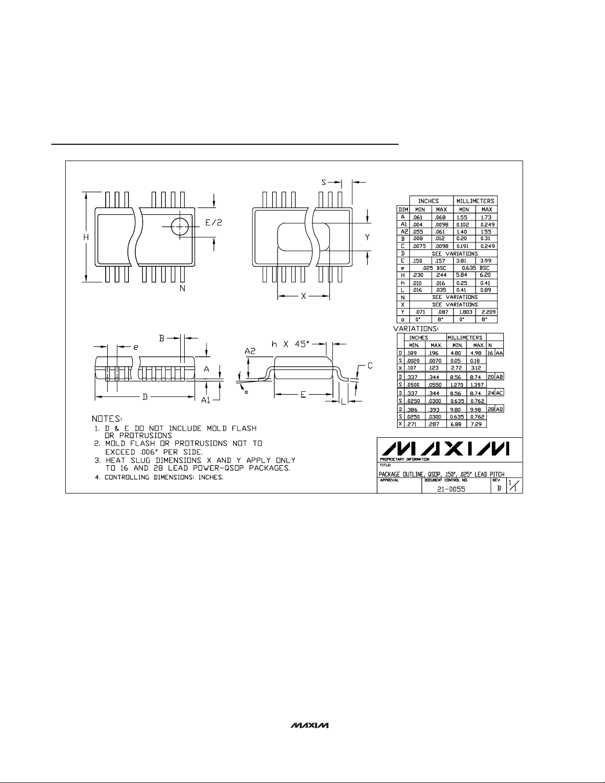
MAX1739/MAX1839
†
Wide Brightness Range
CCFL Backlight Controllers
Package Information
Maxim cannot assume responsibility for use of any circuitry other than circuitry entirely embodied in a Maxim product. No circuit patent licenses are
implied. Maxim reserves the right to change the circuitry and specifications without notice at any time.
26 ____________________Maxim Integrated Products, 120 San Gabriel Drive, Sunnyvale, CA 94086 408-737-7600
© 2001 Maxim Integrated Products Printed USA is a registered trademark of Maxim Integrated Products.
QSOP.EPS
 Loading...