

Page 1
For price, delivery, and to place orders, please contact Maxim Distribution at 1-888-629-4642,
or visit Maxim’s website at www.maxim-ic.com.
General Description
The MAX1832–MAX1835 are high-efficiency step-up
converters with complete reverse battery protection that
protects the device and the load when the battery is
reversed. They feature a built-in synchronous rectifier,
which allows for over 90% efficiency and reduces size
and cost by eliminating the need for an external
Schottky diode.
These step-up converters operate from a +1.5V to
+5.5V input voltage range and deliver up to 150mA of
load current. The MAX1833/MAX1835 have a fixed
+3.3V output, and the MAX1832/MAX1834 have
adjustable outputs from +2V to +5.5V. In shutdown, the
MAX1832/MAX1833 connect the battery input to the
voltage output, allowing the input battery to be used as
a backup or real-time clock supply when the converter
is off (see Selector Guide).
The MAX1832–MAX1835 are available in a miniature 6pin SOT23 package. The MAX1832EVKIT is available to
shorten the design cycle.
________________________Applications
Medical Diagnostic Equipment
Pagers
Hand-Held Instruments
Remote Wireless Transmitters
Digital Cameras
Cordless Phones
Battery Backup
PC Cards
Local 3.3V or 5V Supply
Features
♦ Reverse Battery Protection for DC-DC Converter
and Load
♦ Up to 90% Efficiency
♦ No External Diode or FETs Needed
♦ Internal Synchronous Rectifier
♦ 4µA Quiescent Current
♦ <1µA Shutdown Supply Current
♦ +1.5V to +5.5V Input Voltage Range
♦ Accurate SHDN Threshold for Low-Battery Cutoff
♦ BATT Connected to OUT in Shutdown for Backup
Power (MAX1832/MAX1833)
♦ RST Output (MAX1833/MAX1835)
♦ Fixed +3.3V Output Voltage (MAX1833/MAX1835)
♦ Adjustable Output Voltage (MAX1832/MAX1834)
♦ Up to 150mA Output Current
♦ Tiny 6-Pin SOT23 Package
MAX1832–MAX1835
High-Efficiency Step-Up Converters with
Reverse Battery Protection in SOT23-6
________________________________________________________________ Maxim Integrated Products 1
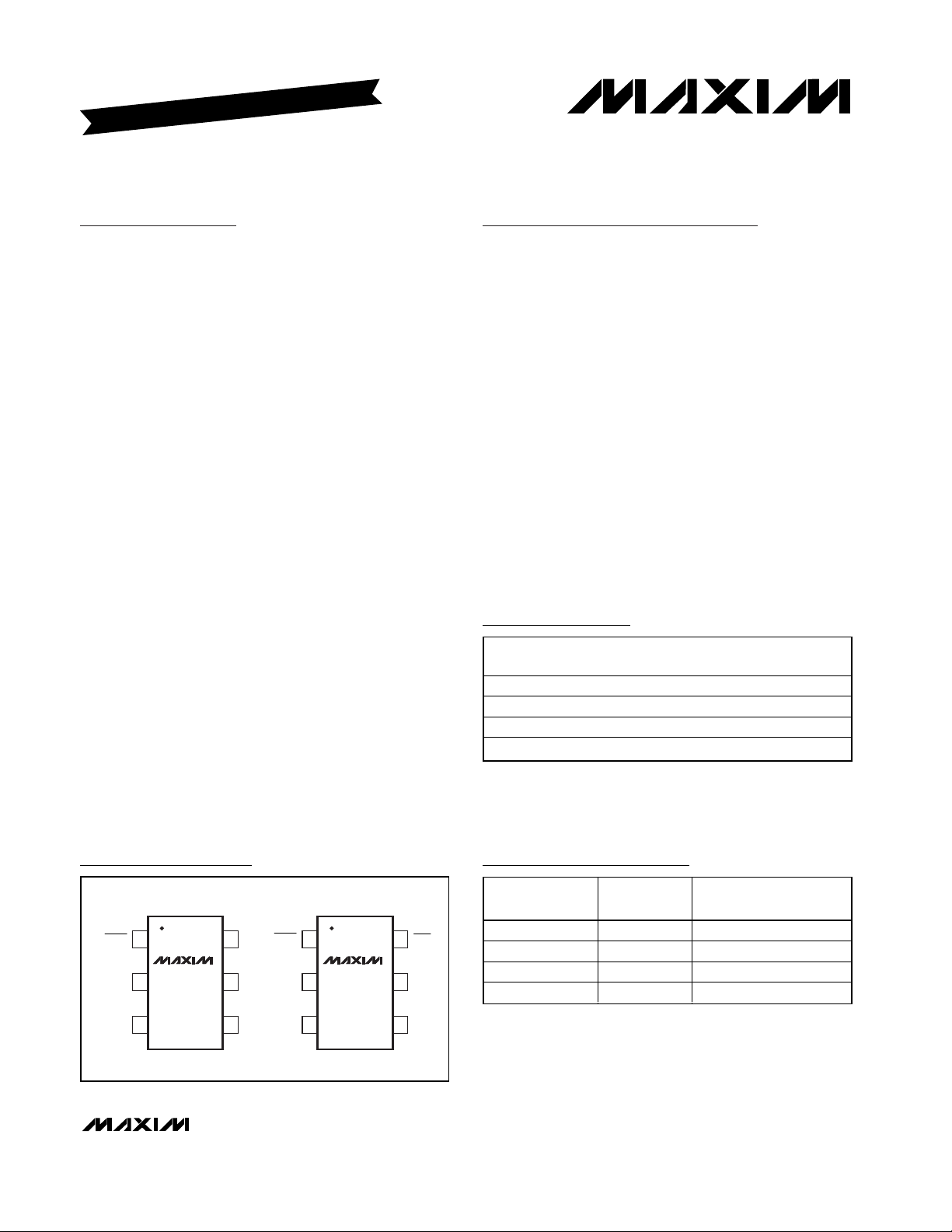
Pin Configurations
19-1802; Rev 0; 10/00
EVALUATION KIT AVAILABLE
Ordering Information
Selector Guide
Note: Requires special solder temperature profile described in
the Absolute Maximum Ratings.
PART T EM P. R A N G E
MAX1832EUT-T -40°C to +85°C 6 SOT23-6 AAOT
MAX1833EUT-T -40°C to +85°C 6 SOT23-6 AAOU
MAX1834EUT-T -40°C to +85°C 6 SOT23-6 AAOV
MAX1835EUT-T -40°C to +85°C 6 SOT23-6 AAOW
PINPACKAGE
TOP
MARK
TOP VIEW
16FB
SHDN
BATT
MAX1832
2
MAX1834
34
SOT23-6
5 OUT
16RST
SHDN
BATT
LXGND
MAX1833
2
MAX1835
34
SOT23-6
5 OUT
LXGND
PART
MAX1832EUT-T Adjustable V
MAX1833EUT-T Fixed 3.3V V
MAX1834EUT-T Adjustable V
MAX1835EUT-T Fixed 3.3V V
OUTPUT
VOLTAGE
OUTPUT VOLTAGE
IN SHUTDOWN
BATT
BATT
- 0.7V
BATT
- 0.7V
BATT
Page 2
MAX1832–MAX1835
High-Efficiency Step-Up Converters with
Reverse Battery Protection in SOT23-6
2 _______________________________________________________________________________________
ABSOLUTE MAXIMUM RATINGS
ELECTRICAL CHARACTERISTICS
(V
SHDN
= +1.5V, V
OUT
= +3.3V, V
BATT
= +2V, GND = 0, TA= -40°C to +85°C. Typical values are at TA= +25°C, unless otherwise
noted.) (Note 3)
Stresses beyond those listed under “Absolute Maximum Ratings” may cause permanent damage to the device. These are stress ratings only, and functional
operation of the device at these or any other conditions beyond those indicated in the operational sections of the specifications is not implied. Exposure to
absolute maximum rating conditions for extended periods may affect device reliability.
BATT, LX to GND.........................................................-6V to +6V
LX to OUT ....................................................................-6V to +1V
SHDN to GND..............................................-6V to (V
OUT
+ 0.3V)
OUT, FB, RST TO GND ............................................-0.3V to +6V
LX Current ................................................................................1A
Continuous Power Dissipation (T
A
= +70°C)
SOT23-6 (derate 9.1mW/°C above +70°C) (Note 1)....727mW
Operating Temperature Range ...........................-40°C to +85°C
Junction Temperature......................................................+150°C
Storage Temperature Range .............................-65°C to +150°C
Lead Temperature (soldering, 10s) (Note 2) ...................+300°C
Note 1: Thermal properties are specified with product mounted on PC board with one square-inch of copper area and still air.
Note 2: This device is constructed using a unique set of packaging techniques that impose a limit on the thermal profile the device
can be exposed to during solder attach and rework. This limit permits only the use of the solder profiles recommended in
the industry-standard specification, IPC/JEDEC J-STD-020A, paragraph 7.6, Table 3 for the IR/VPR and Convection reflow.
Preheating is required. Hand or wave soldering is not allowed.
PARAMETER SYMBOL CONDITIONS MIN TYP MAX UNITS
Output Range V
Battery Input Range V
Startup Battery Input Voltage V
Output Voltage V
FB Trip Voltage V
FB Input Bias Current I
N-Channel On-Resistance R
P-Channel On-Resistance R
OUT
BATT
SU
OUT
FB
FB
NCH
PCH
P-Channel Catch-Diode Voltage
N-Channel Switch Current Limit I
Switch Maximum On-Time t
MAX
ON
Synchronous Rectifier ZeroCrossing Current
Quiescent Current into OUT
(Note 4)
Shutdown Current into OUT V
MAX1832/MAX1834 2.0 5.5 V
R
= 2.6kΩ
LOAD
MAX1833/
MAX1835
MAX1832/
MAX1834
MAX1832/
MAX1834,
V
= +1.3V
FB
V
= +3.3V
OUT
I
= 100mA
LX
V
= +3.3V
OUT
I
= 100mA
LX
I
= 100mA, PCH off, V
LX
V
= +1.3V
FB
V
= +3.3V
OUT
= +3.3V
V
OUT
V
= +3.5V,
OUT
V
= +1.3V
FB
= +3.5V, V
OUT
1.5 5.5 V
T
= +25°C 1.22 1.5
A
= -40°C to +85°C 1.24
T
A
T
= +25°C 3.225 3.290 3.355
A
= -40°C to +85°C 3.208 3.372
T
A
T
= +25°C 1.208 1.228 1.248
A
= -40°C to +85°C 1.204 1.252
T
A
T
= +25°C 3.5 20
A
= -40°C to +85°C 4.0
T
A
T
= +25°C 0.4 1.2
A
T
= -40°C to +85°C 1.5
A
T
= +25°C 0.5 1.3
A
T
= -40°C to +85°C 1.6
A
= +3.5V,
OUT
T
= +25°C 435 525 615
A
= -40°C to +85°C 400 650
T
A
0.73 V
3.5 5 6.5 µs
T
= +25°C 2 17 34
A
T
= -40°C to +85°C0 39
A
T
= +25°C 2.5 7.0
A
T
= -40°C to +85°C 8.0
A
= VFB = 0V 0.05 1 µA
SHDN
V
V
V
nA
Ω
Ω
mA
mA
µA
Page 3

MAX1832–MAX1835
High-Efficiency Step-Up Converters with
Reverse Battery Protection in SOT23-6
_______________________________________________________________________________________ 3
Note 3: All units are 100% production tested at TA=+25°C. Limits over the operating temperature range are guaranteed by design
and not production tested.
Note 4: Supply current into OUT. This current correlates directly to the actual battery-supply current, but is reduced in value accord-
ing to the step-up ratio and efficiency.
ELECTRICAL CHARACTERISTICS (continued)
(V
SHDN
= +1.5V, V
OUT
= +3.3V, V
BATT
= +2V, GND = 0, TA= -40°C to +85°C. Typical values are at TA= +25°C, unless otherwise
noted.) (Note 3)
PARAMETER SYMBOL CONDITIONS MIN TYP MAX UNITS
Reverse Battery Current into
OUT
Quiescent Current into BATT
Shutdown Current into BATT V
Reverse Battery Current into
BATT
SHDN Logic Low V
SHDN Threshold Rising edge
= 0, V
V
OUT
V
= +3.5V,
OUT
= +1.3V
V
FB
= +3.5V, V
OUT
V
= 0, V
OUT
= +1.5V to +5.5V 0.3 V
BATT
BATT
BATT
= V
T
T
BATT
= V
T
T
= VLX = -3V 0 10 µA
SHDN
= +25°C 1.8 5.0
A
= -40°C to +85°C 6.0
A
= +2V, V
= VLX = -3V 0.002 10 µA
SHDN
= +25°C 1.185 1.228 1.271
A
= -40°C to +85°C 1.170 1.286
A
= 0 0.001 1 µA
SHDN
SHDN Threshold Hysteresis 0.02 V
SHDN Input Bias Current V
SHDN Reverse Battery Current V
RST Threshold
RST Voltage Low I
RST Leakage Current V
LX Leakage Current V
LX Reverse Battery Current V
Maximum Load Current I
LOAD
Efficiency V
= +5.5V, V
OUT
= 0, V
OUT
MAX1833/
MAX1835,
falling edge
= 1mA, V
RST
= +5.5V
RST
= +5.5V
LX
= 0, V
OUT
V
= +2V, V
BATT
= +2V, V
BATT
= +5.5V, T
SHDN
BATT
OUT
BATT
= V
= V
OUT
OUT
= VLX = -3V 52 150 µA
SHDN
T
= +25°C 2.830 2.980 3.110
A
T
= -40°C to +85°C 2.800 3.140
A
= +2.5V 0.2 V
T
= +25°C 0.1 100
A
= -40°C to +85°C1
T
A
= +25°C 1 100
T
A
= -40°C to +85°C 100
T
A
= VLX = -3V 0.001 10 µA
SHDN
= +3.3V 150 mA
= +3.3V, I
= +25°C 13 100 nA
A
= 40mA 90 %
LOAD
µA
V
V
nA
nA
Page 4

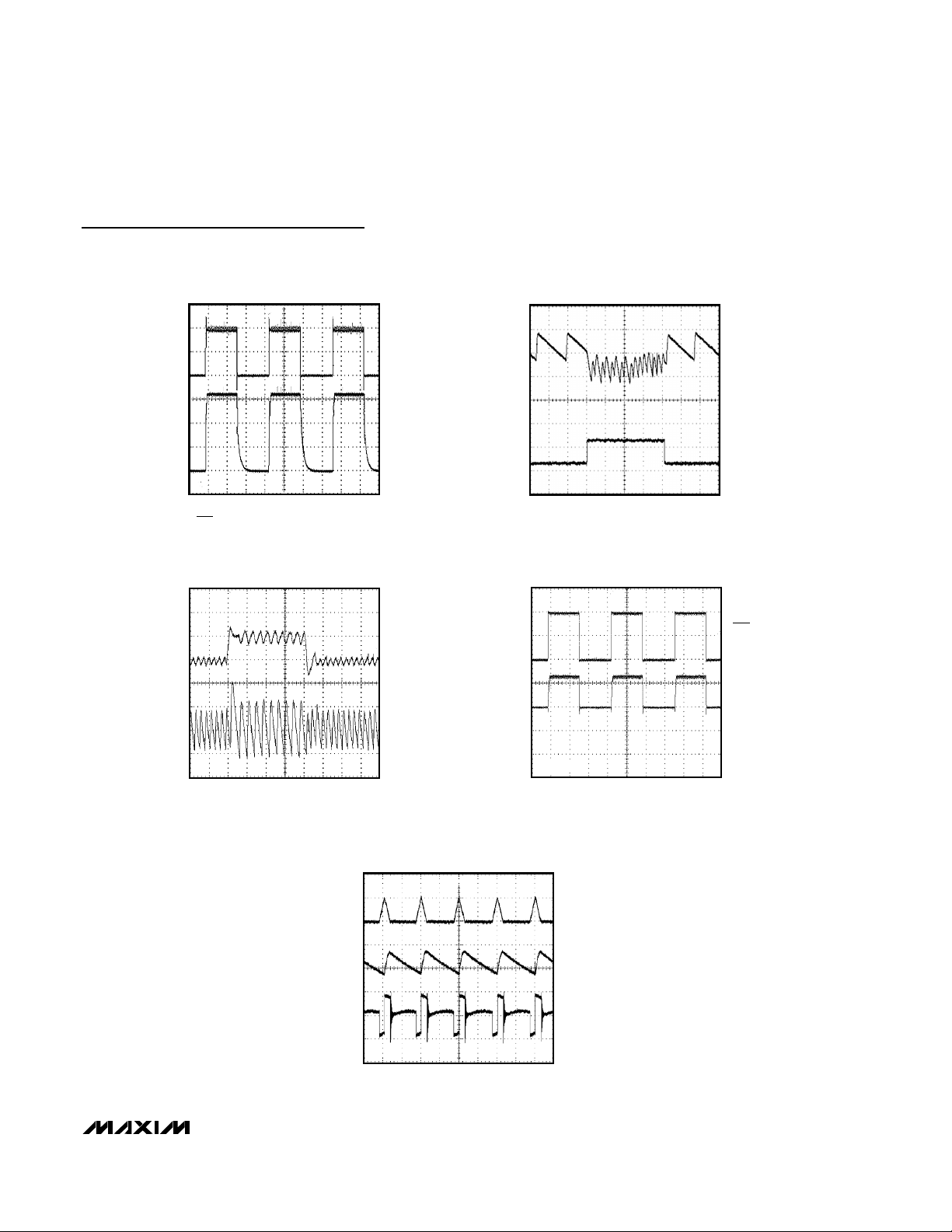
Typical Operating Characteristics
(V
OUT
= +3.3V, V
BATT
= +2V, unless otherwise noted.) (Figure 1)
95
65
0.1 10 1001 1000
EFFICIENCY vs. LOAD CURRENT
(V
OUT
= 5.0V)
MAX1832/35 toc01
I
LOAD
(mA)
EFFICIENCY (%)
70
75
80
85
90
V
BATT
= +1.5V
V
SHDN
= V
BATT
R1 = 309Ω
R2 = 100kΩ
MAX1834
V
BATT
= +2.7V
V
BATT
= +3.3V
0.1 101 100 1000
EFFICIENCY vs. LOAD CURRENT
(V
OUT
= 3.3V)
MAX1832/35 toc02
I
LOAD
(mA)
EFFICIENCY (%)
95
75
80
85
90
V
BATT
= +2.7V
V
BATT
= +1.5V
V
BATT
= +2.0V
V
SHDN
= V
BATT
MAX1835
0.1 101 10 100
EFFICIENCY vs. LOAD CURRENT
(V
OUT
= 2.5V)
MAX1832/35 toc03
I
LOAD
(mA)
EFFICIENCY (%)
85
70
75
80
V
BATT
= +2.0V
V
BATT
= +1.5V
V
SHDN
= V
BATT
R1 = 100kΩ
R2 = 100kΩ
C
IN
= 20µF
C
OUT
= 20µF
MAX1834
0
50
150
100
200
250
132456
MAXIMUM OUTPUT CURRENT
vs. BATTERY VOLTAGE
MAX1832/35 toc04
V
BATT
(V)
I
LOAD
(mA)
V
OUT
= +3.3V
V
OUT
= +5.0V
V
OUT
= +2.5V
1.2
10 10k1k100
STARTUP BATTERY VOLTAGE
vs. LOAD RESISTANCE
1.7
1.4
1.3
1.6
1.5
MAX1832/35 toc05
R
LOAD
(Ω)
V
BATT
(V)
V
SHDN
= V
BATT
V
OUT
= +5.0V
V
OUT
= +3.3V
V
OUT
= +2.5V
-0.2
0.2
0
0.6
0.4
1.0
0.8
1.2
-6 -4 -3 -2-5 -10123456
INPUT CURRENT AND OUTPUT VOLTAGE
vs. BATTERY VOLTAGE (SHUTDOWN, NO LOAD)
MAX1832/35 toc06
V
BATT
(V)
I
BATT
(µA)
I
BATT
V
SHDN
= 0
R
LOAD
= ∞
MAX1833
V
OUT
5
4
3
2
1
0
6
-1
V
OUT
(V)
-50
50
0
150
100
250
200
300
-6 -4 -3 -2-5 -10123456
INPUT CURRENT AND OUTPUT VOLTAGE
vs. BATTERY VOLTAGE (SHUTDOWN, LOADED)
MAX1832/35 toc07
V
BATT
(V)
I
BATT
(mA)
I
BATT
V
SHDN
= 0
R
LOAD
= 22Ω
MAX1833
V
OUT
5
4
3
2
1
0
6
-1
V
OUT
(V)
-20
60
0
100
80
140
120
160
-6 -4 -3 -2-5 -10123456
INPUT CURRENT AND OUTPUT VOLTAGE
vs. BATTERY VOLTAGE (ON, NO LOAD)
MAX1832/35 toc08
V
BATT
(V)
I
BATT
(µA)
I
BATT
3.5
3.0
2.5
1.5
0.5
0
4.0
-0.5
V
OUT
(V)
40
20
V
SHDN
=
V
BATT
R
LOAD
= ∞
R3 = 1MΩ
R4 = 220kΩ
C1 = 10nF
V
OUT
2.0
1.0
I
BATT
MAX1832–MAX1835
High-Efficiency Step-Up Converters with
Reverse Battery Protection in SOT23-6
4 _______________________________________________________________________________________
INPUT CURRENT AND OUTPUT VOLTAGE
vs. BATTERY VOLTAGE (ON, LOADED)
300
V
=
V
SHDN
BATT
V
= 3.3V
OUT
250
200
150
(mA)
BATT
I
100
-50
= 22Ω
R
LOAD
R3 = 1MΩ
R4 = 220kΩ
C1 = 10nF
I
BATT
50
0
-6 -4 -3 -2-5 -10123456
V
BATT
(V)
MAX1832/35 toc09
V
OUT
6
5
4
3
(V)
OUT
V
2
1
0
-1
Page 5
MAX1832–MAX1835
High-Efficiency Step-Up Converters with
Reverse Battery Protection in a SOT23-6
_______________________________________________________________________________________ 5
Typical Operating Characteristics (continued)
(V
OUT
= +3.3V, V
BATT
= +2V, unless otherwise noted.) (Figure 1)
V
V
SHDN
OUT
= V
= 3.3V
BATT
ON/OFF RESPONSE
2ms/div
= 2.0V, R
LOAD
LINE TRANSIENT
= 22Ω,
MAX1832/35 toc10
MAX1832/35 toc12
V
1V/div
V
1V/div
V
500mV/div
BATT
OUT
BATT
LOAD TRANSIENT
R
= 22Ω TO 200Ω,
LOAD
= +3.3V, V
V
OUT
BATT
SHUTDOWN RESPONSE
40µs/div
= +2.0V
MAX1832/35 toc11
MAX1832/35 toc13
V
OUT
100mV/div
I
LOAD
100mA/div
0
V
SHDN
1V/div
0
V
OUT
1V/div
V
OUT
I
= 100mA, V
OUT
= +2.0V TO +2.5V
V
BATT
OUT
40µs/div
= +3.3V,
50mV/div
SWITCHING WAVEFORMS
I
OUT
= 40mA, V
= +3.3V, V
OUT
10µs/div
BATT
MAX1832/35 toc14
= +2.0V
MAX1833
R
LOAD
= 22Ω, V
V
LX
500mA/div
V
OUT
100mV/div
V
LX
2V/div
BATT
40µs/div
= 3.3V, V
BATT
= 2.0V
0
Page 6

MAX1832–MAX1835
High-Efficiency Step-Up Converters with
Reverse Battery Protection in SOT23-6
6 _______________________________________________________________________________________
Pin Description
Figure 1a. MAX1833/MAX1835 Typical Operating Circuit
Figure 1b. MAX1832/MAX1834 Typical Operating Circuit
PIN
MAX1832
MAX1834
MAX1833
MAX1835
11
NAME FUNCTION
SHDN
2 2 BATT Battery Voltage Connection. BATT has reverse battery protection.
3 3 GND Ground
44LX
5 5 OUT
6 — FB
— 6
+1.5V TO +3.3V
BATTERY
10µF
220kΩ
1MΩ
10µH
R4
C1
R3
10nF
LX
SHDN
BATT
MAX1833
MAX1835
RST
OUT
100kΩ
RST
GND
S hutd ow n. A hi g h l og i c l evel tur ns on the d evi ce. W hen SHD N i s l ow the p ar t i s off,
and the cur r ent i nto BATT i s typ i cal l y 0.1µA. For the M AX 1832/M AX 1833, the
b atter y i s connected to OU T thr oug h an i nter nal P FE T and the exter nal i nd uctor
w hen SHD N i s l ow . SHD N can b e used for l ow - b atter y cutoff ( 1.228V thr eshol d ) .
S ee Low - Batter y C utoff. SHD N has r ever se b atter y p r otecti on.
Inductor Connection. N-channel MOSFET switch drain and synchronous
rectifier P-channel switch drain. LX has reverse battery protection.
Output Voltage. Bootstrapped supply for the device. Output sense point for
MAX1833/MAX1835.
MAX1832/MAX1834 Feedback Input. Set the output voltage through a
resistor-divider network. See Setting the Output Voltage.
MAX1833/MAX1835 Power-On Reset Open-Drain Output. RST pulls low when
the output is 10% below the regulation point. If not used, connect to GND.
+1.5V TO +5.0V
BATTERY
OUTPUT
+3.3V
10µF
POWER-ON
RESET
10µF
220kΩ
1MΩ
10µH
R4
R3
C1
10nF
LX
SHDN
BATT
MAX1832
MAX1834
GND
OUT
OUTPUT
+5.0V
R2
309kΩ
FB
R1
100kΩ
Page 7

Detailed Description
The MAX1832–MAX1835 compact, high-efficiency
step-up converters feature 4µA quiescent supply current to ensure the highest possible efficiency over a
wide load range. With a minimum +1.5V input voltage,
these devices are well suited for applications with two
alkaline cells, two nickel-metal-hydride (NiMH) cells, or
one lithium ion (Li+) cell. For the MAX1832 and
MAX1833, the battery is connected to OUT through the
inductor and an internal PFET when SHDN is low. This
allows the input battery to be used as a backup or realtime clock supply when the converter is off by eliminating the voltage drop across the PFET body diode.
The MAX1832–MAX1835 are ideal for low-power applications where ultra-small size is critical. These devices
feature built-in synchronous rectification that significantly improves efficiency and reduces size and cost
by eliminating the need for an external Schottky diode.
Furthermore, these devices are the industry’s first boost
regulators to offer complete reverse battery protection.
This proprietary design protects the battery, IC, and the
circuitry powered by the IC in the event the input batteries are connected backwards.
Control Scheme
A current-limited control scheme is a key feature of the
MAX1832–MAX1835. This scheme provides ultra-low
quiescent current and high efficiency over a wide output current range. There is no oscillator. The inductor
current is limited by the 0.5A N-channel current limit or
by the 5µs switch maximum on-time. Following each
on-cycle, the inductor current must ramp to zero before
another cycle may start. When the error comparator
senses that the output has fallen below the regulation
threshold, another cycle begins.
An internal synchronous rectifier eliminates the need for
an external Schottky diode reducing cost and board
space. While the inductor discharges, the P-channel
MOSFET turns on and shunts the MOSFET body diode.
As a result, the rectifier voltage drop is significantly
reduced, improving efficiency without adding external
components.
Reverse Battery Protection
The MAX1832–MAX1835 have a unique proprietary
design that protects the battery, IC, and circuitry powered by the IC in the event that the input batteries are
connected backwards. When the batteries are connected correctly, the reverse battery protection N-channel
MOSFET is on and the device operates normally.
When the batteries are connected backwards, the
reverse battery protection N-channel MOSFET opens,
protecting the device and load (Figures 2 and 3).
Previously, this level of protection required additional
circuitry and reduced efficiency due to added components in the battery current path.
Applications Information
Shutdown
When SHDN is low, the device is off and no current is
drawn from the battery. When SHDN is high, the device
is on. If SHDN is driven from a logic-level output, the
logic high (on) level should be referenced to V
OUT
to
avoid intermittent turn on. If SHDN is not used at all,
connect it to OUT. With SHDN connected to OUT, the
MAX1834/MAX1835 startup voltage (1.65V) is slightly
higher, due to the voltage across the PFET body diode.
The SHDN pin has reverse battery protection.
In shutdown, the MAX1832/MAX1833 connect the battery input to the output through the inductor and the
internal synchronous rectifier PFET. This allows the
input battery (rather than a separate backup battery) to
provide backup power for devices such as an idled
microcontroller, SRAM, or real-time clock, without the
usual diode forward drop. If the output has a residual
voltage during shutdown, a small amount of energy will
be transfered from the output back to the input immediately after shutdown. This energy transfer may cause a
slight momemntary “bump” in the input voltage. The
magnitude and duration of the input bump are related
to the ratio of C
IN
and C
OUT
and the ability of the input
to sink current. With battery input sources, the bump
will be negligible, but with power-supply inputs (that
typically cannot sink current), the bump may be 100s of
mV.
In shutdown, the MAX1834/MAX1835 do not turn on the
internal PFET and thus do not have an output-to-input
current path in shutdown. This allows a separate backup battery, such as a Li+ cell, to be diode-connected at
the output, without leakage current flowing to the input.
The MAX1834/MAX1835 still have the typical input-tooutput current path from the battery to the output,
through the PFET body diode, in shutdown.
Low-Battery Cutoff
The SHDN trip threshold of the MAX1832–MAX1835
can be used as a voltage detector, with a resistordivider, to power down the IC when the battery voltage
falls to a set level (Figure 1). The SHDN trip threshold is
1.228V. To use a resistor-divider to set the shutdown
voltage, select a value for R3 in the 100kΩ to 1MΩ
MAX1832–MAX1835
High-Efficiency Step-Up Converters with
Reverse Battery Protection in SOT23-6
_______________________________________________________________________________________ 7
Page 8

MAX1832–MAX1835
High-Efficiency Step-Up Converters with
Reverse Battery Protection in SOT23-6
8 _______________________________________________________________________________________
Figure 3. MAX1833/MAX1835 Simplified Functional Diagram
Figure 2. MAX1832/MAX1834 Simplified Functional Diagram
OUT
ZEROCROSSING
DETECTOR
DRIVER
P
LX
SHDN
STARTUP
CIRCUITRY
MAX1832
MAX1834
CONTROL
LOGIC
FB
ERROR
COMPARATOR
1.228V
OUT
ERROR
COMPARATOR
1.228V
STARTUP
CIRCUITRY
MAX1833
MAX1835
CONTROL
LOGIC
REVERSE BATTERY
PROTECTION MOSFET
CURRENT
LIMIT
CROSSING
DETECTOR
DRIVER
REVERSE BATTERY
PROTECTION MOSFET
N
ZERO-
N
GND
BATT
P
LX
N
BATT
N
RST
SHDN
N
RESET
1.1V
CURRENT
LIMIT
GND
Page 9

MAX1832–MAX1835
High-Efficiency Step-Up Converters with
Reverse Battery Protection in SOT23-6
_______________________________________________________________________________________ 9
range to minimize battery drain. Calcuate R4 as follows:
R4 = R3 ✕(V
OFF
/ V
SHDN
- 1)
V
OFF
is the battery voltage at which the part will shut
down and V
SHDN
= 1.228V. Note that input ripple can
sometimes cause false shutdowns. To minimize the effect
of ripple, connect a low-value capacitor (C1) from SHDN
to GND to filter out input noise. Select a C1 value such
that the R4
✕
C1 time constant is above 2ms.
Power-On Reset
The MAX1833/MAX1835 provide a power-on reset output (RST). A 100kΩ to 1MΩ pullup resistor from RST to
OUT provides a logic control signal. This open-drain
output pulls low when the output is 10% below its regulation point. If not used, connect it to GND.
Setting the Output Voltage
The output voltage of the MAX1832/MAX1834 is
adjustable from +2V to +5.5V, using external resistors
R1 and R2 (Figure 1b). Since FB leakage is 20nA
(max), select feedback resistor R1 to be 100kΩ to
1MΩ. Calculate R2 as follows:
where V
FB
= 1.228V.
Inductor Selection
The control scheme of the MAX1832–MAX1835 permits
flexibility in choosing an inductor. A 10µH inductor performs well for most applications, but values from 4.7µH
to 100µH may also be used. Small inductance values
typically offer smaller physical size. Large inductance
values minimize output ripple but reduce output power.
Output power is reduced when the inductance is large
enough to prevent the maximum current limit (525mA)
from being reached before the maximum on-time (5µs)
expires.
For maximum output current, choose L such that:
where R
IND
is the inductor series resistance, and R
NCH
is the R
DS(ON)
of the N-channel MOSFET (0.4Ω typ).
Capacitor Selection
Choose an output capacitor to achieve the desired output ripple percentage.
where r is the desired output ripple in %. A 10µF ceramic
capacitor is a good starting value. The input capacitor
reduces the peak current drawn from the battery and
can be the same value as the input capacitor. A larger
input capacitor can be used to further reduce ripple and
improve efficiency.
PC Board Layout and Grounding
Careful printed circuit layout is important for minimizing
ground bounce and noise. Keep the IC’s GND pin and
the ground leads of the input and output filter capacitors less than 0.2in (5mm) apart. In addition, keep all
connections to the FB and LX pins as short as possible.
In particular, when using external feedback resistors,
Table 1. Suggested Inductors and
Suppliers
Table 2. Suggested Surface-Mount
Capacitors and Manufacturers
V
RR
21 1=−
OUT
V
FB
I
OUT MAX
Vs
BATT MAX BATT MIN() ()
0 525
.
()
0 525
=
1
µµ
()
A
..
V
BATT MIN NCH IND
A
×
2
Vs
<<
L
−+
()
0 525
.
0 525
2
V
OUT
5
()
A
A
RR
()
MANUFACTURER INDUCTOR PHONE
Coilcraft
Sumida
Murata LQH4N100K 814-237-1431
DS1608C-103
DO1606T-103
CDRH4D18-100
CR43-100
847-639-6400
847-956-0666
VALUE
(µF)
4.7 to
47
4.7 to
10
4.7 to
22
DESCRIPTION
594/595 D-
series tantalum
TAJ, TPS-
series tantalum
X7R ceramic TDK 847-390-4373
X7R ceramic Taiyo Yuden 408-573-4150
C
05 0525
>
OUT
MANU-
FACTURER
Sprague 603-224-1961
AVX 803-946-0690
LA
××
..
rV
×
%
OUT
2
2
PHONE
Page 10

Maxim cannot assume responsibility for use of any circuitry other than circuitry entirely embodied in a Maxim product. No circuit patent licenses are
implied. Maxim reserves the right to change the circuitry and specifications without notice at any time.
Maxim Integrated Products, 120 San Gabriel Drive, Sunnyvale, CA 94086 408-737-7600 ____________________ 10
© 2000 Maxim Integrated Products Printed USA is a registered trademark of Maxim Integrated Products.
Package Information
MAX1832–MAX1835
High-Efficiency Step-Up Converters with
Reverse Battery Protection in SOT23-6
6LSOT.EPS
 Loading...