

Page 1
General Description
The MAX1820/MAX1821 low-dropout, pulse-width-modulated (PWM) DC-DC buck regulators are optimized to
provide power to the power amplifier (PA) in WCDMA
cell phones; however, they may be applied in many
other applications where high efficiency is a priority. The
supply voltage range is from 2.6V to 5.5V, and the guaranteed output current is 600mA; 1MHz PWM switching
allows for small external components, while skip mode
reduces quiescent current to 180µA with light loads.
The MAX1820 is dynamically controlled to provide varying output voltages from 0.4V to 3.4V. The circuit is
designed such that the output voltage settles in <30µs
for a full-scale change in voltage and current. The
MAX1821 is set with external resistors to provide any
fixed output voltage in the 1.25V to 5.5V range.
The MAX1820/MAX1821 include a low on-resistance
internal MOSFET switch and synchronous rectifier to
maximize efficiency and minimize external component
count; 100% duty-cycle operation allows for low dropout
of only 150mV at 600mA load, including the external
inductor resistance. The devices are offered in 10-pin
µMAX and tiny 3✕ 4 chip-scale (UCSP™) packages.
________________________Applications
WCDMA Cell Phone Power Amplifiers
PDA, Palmtop, and Notebook Computers
Microprocessor Core Supplies
Digital Cameras
PCMCIA and Network Cards
Hand-Held Instruments
Features
♦ Dynamically Adjustable Output from 0.4V to 3.4V
(MAX1820)
♦ Programmable Output from 1.25V to 5.5V
(MAX1821)
♦ SYNC to 13MHz External Clock (MAX1820X)
♦ SYNC to 19.8MHz External Clock (MAX1820Y)
♦ NO SYNC, Internal 1MHz Oscillator (MAX1820Z)
♦ Low Quiescent Current
180µA (typ) in Skip Mode
0.1µA (typ) in Shutdown Mode
♦ No External Schottky Diode Required
♦ 600mA Guaranteed Output Current
♦ 0% to 100% Duty-Cycle Operation
♦ 150mV Dropout at 600mA Load (Including R
DC
of External Inductor)
♦ µMAX or UCSP Packaging
MAX1820/MAX1821
WCDMA Cellular Phone 600mA
Buck Regulators
________________________________________________________________ Maxim Integrated Products 1
19-2011; Rev 2; 7/02
EVALUATION KIT
AVAILABLE
Ordering Information
For pricing, delivery, and ordering information, please contact Maxim/Dallas Direct! at
1-888-629-4642, or visit Maxim’s website at www.maxim-ic.com.
Pin Configurations appear at end of data sheet.
Typical Operating Circuits continued at end of data sheet.
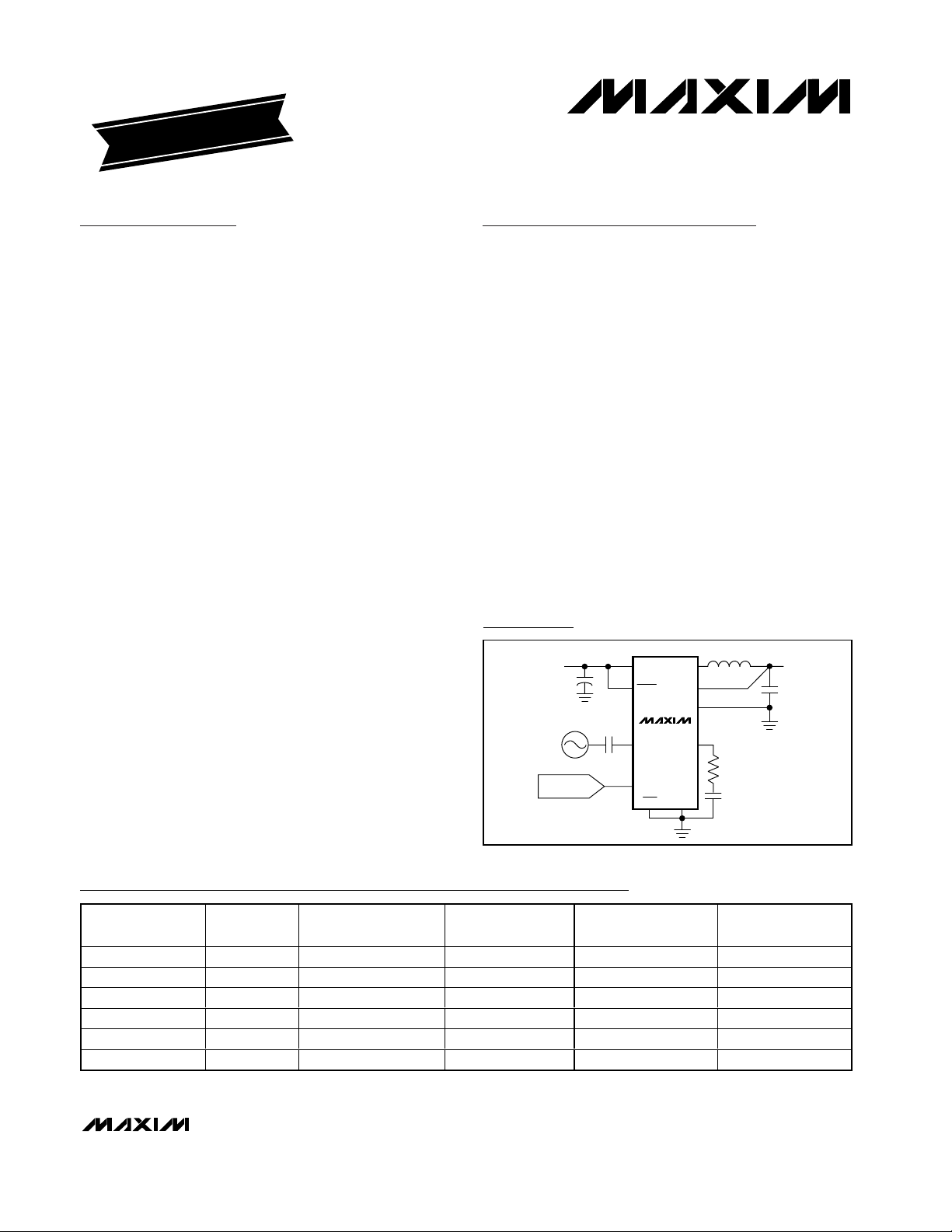
SYNC
GND
SHDN
BATT
PGND
COMP
V
OUT
CONTROL
DAC
REF
LX
OUT
13MHz
OR
19.8MHz
MAX1820
SKIP
4.7µH
4.7µF
INPUT
2.6V TO
5.5V
DYNAMIC
OUTPUT
0.4V TO 3.4V
Typical Operating Circuits
*UCSP reliability is integrally linked to the user’s assembly methods, circuit board material, and environment. Refer to the UCSP
Reliability Notice in the UCSP Reliability section of this data sheet for more information.
UCSP is a trademark of Maxim Integrated Products, Inc.
Ordering Information continued at end of data sheet.
PART
MAX1820ZEBC*
MAX1820YEBC*
MAX1820XEBC*
MAX1820ZEUB
MAX1820YEUB
MAX1820XEUB
SYNC
FREQ (MHz)
No Sync
19.8
13
No Sync
19.8
13
OUTPUT VOLTAGE TEMP RANGE PIN-PACKAGE UCSP MARK
✕
4 UCSP AAB
✕
4 UCSP AAL
✕
4 UCSP AAM
Dynamic -40°C to +85°C3
Dynamic -40°C to +85°C3
Dynamic -40°C to +85°C3
Dynamic -40°C to +85°C 10 µMAX —
Dynamic -40°C to +85°C 10 µMAX —
Dynamic -40°C to +85°C10 µMAX —
Page 2

MAX1820/MAX1821
WCDMA Cellular Phone 600mA
Buck Regulators
2 _______________________________________________________________________________________
ABSOLUTE MAXIMUM RATINGS
Stresses beyond those listed under “Absolute Maximum Ratings” may cause permanent damage to the device. These are stress ratings only, and functional
operation of the device at these or any other conditions beyond those indicated in the operational sections of the specifications is not implied. Exposure to
absolute maximum rating conditions for extended periods may affect device reliability.
BATT, OUT (FB), SHDN, SYNC, SKIP,
REF to GND .......................................................-0.3V to +6.0V
PGND to GND .......................................................-0.3V to +0.3V
LX, COMP to GND...................................-0.3V to (V
BATT
+ 0.3V)
Output Short-Circuit Duration ............................................Infinite
Continuous Power Dissipation (T
A
= +70°C)
3
✕
4 UCSP (derate 10.4mW/°C above +70°C)............832mW
10-Pin µMAX (derate 5.6mW/°C above +70°C) ...........444mW
Operating Temperature Range ...........................-40°C to +85°C
Junction Temperature......................................................+150°C
Storage Temperature Ranges
3
✕
4 UCSP ....................................................-40°C to +150°C
10-Pin µMAX ..................................................-65°C to +150°C
Solder Profile (UCSP) ......................................................(Note 1)
Lead Temperature (soldering, 10s) .................................+300°C
ELECTRICAL CHARACTERISTICS
(V
BATT
= 3.6V, SHDN = BATT, SKIP = SYNC = GND, V
REF
= 1.25V (MAX1820 only), TA= 0°C to +85°C, unless otherwise noted.
Typical values are at T
A
= +25°C.) (Note 2)
Note 1: For UCSP solder profile information, visit www.maxim-ic.com/1st_pages/UCSP.htm.
Input BATT Voltage V
Undervoltage Lockout
PARAMETER SYMBOL CONDITIONS MIN TYP MAX UNITS
Threshold
Quiescent Current I
V
UVLO
IN
Q
Quiescent Current in Dropout
Shutdown Supply Current I
SHDN
ERROR AMPLIFIER
OUT Voltage Accuracy
(MAX1820)
OUT Input Resistance
(MAX1820)
V
R
OUT
OUT
V
rising, 1% hysteresis 2.20 2.35 2.55 V
BATT
SKIP = GND (MAX1820Z/MAX1821) 180 300
SKIP = BATT, no switching 450 2000
SKIP = GND (MAX1820Y, MAX1820X, and
MAX1821X)
SKIP = BATT, 1MHz switching 3300
SKIP = GND 530 1000
SKIP = BATT, no switching 550 1000
SHDN = GND 0.1 6 µA
V
= 1.932 ±0.005V, load = 0 to 600mA,
REF
SKIP = BATT or GND
V
= 0.227 ±0.005V, load = 0 to 30mA,
REF
SKIP = BATT, V
2.6 5.5 V
240 360
3.33 3.4 3.47
BATT
≤ 4.2V
0.35 0.40 0.45
250 400 kΩ
µA
µA
V
REF Input Current (MAX1820) I
FB Voltage Accuracy
(MAX1821)
FB Input Current (MAX1821) I
Transconductance g
REF
V
FB
FB
FB = COMP 1.225 1.25 1.275 V
V
= 1.4V 0.01 50 nA
FB
m
30 50 85 µS
0.1 1 µA
COMP Clamp Low Voltage 0.2 0.45 1.0 V
COMP Clamp High Voltage 2.04 2.15 2.28 V
Page 3

MAX1820/MAX1821
WCDMA Cellular Phone 600mA
Buck Regulators
_______________________________________________________________________________________ 3
ELECTRICAL CHARACTERISTICS (continued)
(V
BATT
= 3.6V, SHDN = BATT, SKIP = SYNC = GND, V
REF
= 1.25V (MAX1820 only), TA= 0°C to +85°C, unless otherwise noted.
Typical values are at T
A
= +25°C.) (Note 2)
CONTROLLER
P-Channel On-Resistance P
N-Channel On-Resistance N
Current-Sense Transresistance R
P-Channel Current-Limit
Threshold
P-Channel Pulse-Skipping
Current Threshold
N-Channel Current-Limit
Threshold
LX Leakage Current I
Maximum Duty Cycle duty
Minimum Duty Cycle duty
SYNC AND OSCILLATOR
SYNC Divide Ratio
(MAX1820X)
SYNC Capture Range
(MAX1820X)
SYNC Leakage Current
Frequency
SYNC Divide Ratio
(MAX1820Y)
SYNC Capture Range
(MAX1820Y)
Internal Oscillator Frequency
(MAX1820Z, MAX1821)
LOGIC INPUTS (SKIP, SHDN)
Logic Input High V
Logic Input Low V
Logic Input Current -1 0.1 1 µA
PARAMETER SYMBOL CONDITIONS MIN TYP MAX UNITS
RDS
RDS
LX
I
SYNC
f
OSC
ILX = 180mA, V
ILX = 180mA, V
ILX = 180mA, V
ILX = 180mA, V
CS
Duty factor = 100% 0.75 1.2 1.55 A
SKIP = GND 0.04 0.13 0.24 A
SKIP = BATT -1.6 -0.85 -0.45
SKIP = GND 0.02 0.08 0.14
V
BATT
MAX
SKIP = GND 0
MIN
SKIP = BATT, V
S Y N C = si ne w ave, S Y N C i np ut = 200m V
S Y N C = si ne w ave, S Y N C i np ut = 800m V
SYNC = sine wave, AC-coupled,
SYNC input = 500mV
V
SYNC
V
SYNC
MAX1821X)
S Y N C = si ne w ave, S Y N C i np ut = 200m V
S Y N C = si ne w ave, S Y N C i np ut = 800m V
SYNC = sine wave, AC-coupled,
SYNC input = 500mV
SYNC = GND 0.8 1 1.2 MHz
IH
IL
= 3.6V 0.15 0.3
BATT
= 2.6V 0.2
BATT
= 3.6V 0.2 0.35
BATT
= 2.6V 0.3
BATT
0.25 0.50 0.75 V/A
= 5.5V, LX = GND or BATT -1 0.1 1 µA
100 %
= 4.2V
BATT
= 1V (MAX1820Z, MAX1821) -1 +1
= 1V (MAX1820X, MAX1820Y, and
P-P
P-P
P-P
P-P
P-P
P-P
P-P
13 13
13 13
10 13 16 MHz
-5 +5
18 18
18 18
15 19.8 21 MHz
1.6 V
10
0.4 V
Ω
Ω
A
%
Hz/Hz
µA
Hz/Hz
Page 4

MAX1820/MAX1821
WCDMA Cellular Phone 600mA
Buck Regulators
4 _______________________________________________________________________________________
ELECTRICAL CHARACTERISTICS
(V
BATT
= 3.6V, SHDN = BATT, SKIP = SYNC = GND, V
REF
= 1.25V (MAX1820 only), TA = -40°C to +85°C, unless otherwise noted.)
(Notes 2, 3)
Input BATT Voltage V
Undervoltage Lockout
Threshold
Quiescent Current I
Quiescent Current in Dropout
Shutdown Supply Current I
ERROR AMPLIFIER
OUT Voltage Accuracy
(MAX1820)
OUT Input Resistance
(MAX1820)
REF Input Current (MAX1820) I
FB Voltage Accuracy
(MAX1821)
PARAMETER SYMBOL CONDITIONS MIN MAX UNITS
IN
V
UVLO
Q
SHDN
V
OUT
R
OUT
REF
V
FB
V
BATT
SKIP = GND (MAX1820Z, MAX1821) 300
SKIP = GND (MAX1820X, MAX1820Y, and
MAX1821X)
SKIP = BATT, no switching 2000
SKIP = GND 1000
SKIP = BATT, no switching 1000
SHDN = GND 6 µA
V
REF
SKIP = BATT or GND
V
REF
SKIP = BATT, V
FB = COMP 1.225 1.275 V
rising, 1% hysteresis 2.15 2.55 V
= 1.932 ±0.005V, load = 0 to 600mA,
= 0.227 ±0.005V, load = 0 to 30mA,
≤ 4.2V
BATT
2.6 5.5 V
360
3.33 3.47
0.35 0.45
250 kΩ
1µA
µA
µA
V
FB Input Current (MAX1821) I
Transconductance g
COMP Clamp Low Voltage 0.2 1.0 V
COMP Clamp High Voltage 2.04 2.28 V
CONTROLLER
P-Channel On-Resistance P
N-Channel On-Resistance N
Current-Sense Transresistance R
P-Channel Current-Limit
Threshold
P-Channel Pulse-Skipping
Current Threshold
N-Channel Current-Limit
Threshold
FB
m
RDS
RDS
CS
V
= 1.4V 50 nA
FB
30 85 µS
ILX = 180mA, V
ILX = 180mA, V
Duty factor = 100% 0.75 1.55 A
SKIP = GND 0.04 0.24 A
SKIP = BATT -1.6 -0.45
SKIP = GND 0.01 0.14
= 3.6V 0.3 Ω
BATT
= 3.6V 0.35 Ω
BATT
0.25 0.75 V/A
A
Page 5
MAX1820/MAX1821
WCDMA Cellular Phone 600mA
Buck Regulators
_______________________________________________________________________________________ 5
Note 2: Limits are 100% production tested at TA= +25°C for UCSP parts. Limits over the entire operating temperature range are
guaranteed by design and characterization but are not production tested.
Note 3: Specifications to -40°C are guaranteed by design and not subject to production test.
ELECTRICAL CHARACTERISTICS (continued)
(V
BATT
= 3.6V, SHDN = BATT, SKIP = SYNC = GND, V
REF
= 1.25V (MAX1820 only), TA = -40°C to +85°C, unless otherwise noted.)
(Notes 2, 3)
40
50
60
70
80
90
100
0 1.00.5 1.5 2.0 2.5 3.0 3.5 4.0
EFFICIENCY vs. OUTPUT VOLTAGE
(NORMAL MODE, V
IN
= 3.6V)
MAX1820/21 toc01
OUTPUT VOLTAGE (V)
EFFICIENCY (%)
R
LOAD
= 10Ω
R
LOAD
= 15Ω
R
LOAD
= 5Ω
40
50
60
70
80
90
100
0 1.00.5 1.5 2.0 2.5 3.0 3.5 4.0
EFFICIENCY vs. OUTPUT VOLTAGE
(PWM MODE, V
IN
= 3.6V)
MAX1820/21 toc02
OUTPUT VOLTAGE (V)
EFFICIENCY (%)
R
LOAD
= 10Ω
R
LOAD
= 15Ω
R
LOAD
= 5Ω
0
20
10
40
30
60
50
70
90
80
100
2.0 3.0 3.52.5 4.0 4.5 5.0 5.5 6.0
MAX1820/21 toc03
VIN (V)
EFFICIENCY (%)
EFFICIENCY vs. INPUT VOLTAGE
NORMAL MODE, R
LOAD
= 10Ω
V
OUT
= 1.8V
V
OUT
= 3.4V
V
OUT
= 0.4V
Typical Operating Characteristics
(TA = +25°C, unless otherwise noted.)
LX Leakage Current I
Maximum Duty Cycle duty
Minimum Duty Cycle duty
PARAMETER SYMBOL CONDITIONS MIN MAX UNITS
LX
MAX
V
BATT
SKIP = GND 0
MIN
SKIP = BATT, V
SYNC AND OSCILLATOR
SYNC Divide Ratio
(MAX1820X)
SYNC Capture Range
(MAX1820X)
SYNC Divide Ratio
(MAX1820Y)
SYNC Capture Range
(MAX1820Y)
SYNC Leakage Current I
SYNC
S Y N C = si ne w ave, S Y N C i np ut = 200m V
S Y N C = si ne w ave, S Y N C i np ut = 800m V
SYNC = sine wave, AC-coupled,
SYNC input = 500mV
S Y N C = si ne w ave, S Y N C i np ut = 200m V
S Y N C = si ne w ave, S Y N C i np ut = 800m V
SYNC = sine wave, AC-coupled,
SYNC input = 500mV
V
SYNC
V
SYNC
M AX 1821X )
Internal Oscillator Frequency
(MAX1820Z, MAX1821)
f
OSC
SYNC = GND 0.8 1.2 MHz
LOGIC INPUTS (SKIP, SHDN)
Logic Input High V
Logic Input Low V
IH
IL
Logic Input Current 1µA
= 5.5V, LX = GND or BATT -1 1 µA
100 %
= 4.2V 10
BATT
P-P
P-P
P-P
P-P
P-P
P-P
13 13
13 13
10 16 MHz
18
18
15 21 MHz
= IV ( M AX 1820Z , M AX 1821) -1
= IV ( M AX 1820X , M AX 1820Y , and
18
18
+1
-5 +5
%
Hz/Hz
Hz/Hz
µA
1.6 V
0.4 V
Page 6

MAX1820/MAX1821
WCDMA Cellular Phone 600mA
Buck Regulators
6 _______________________________________________________________________________________
Typical Operating Characteristics (continued)
(TA = +25°C, unless otherwise noted.)
90
0
1 100010010
MAX1821 EFFICIENCY vs. LOAD CURRENT
(V
OUT
= 3.3V)
30
10
70
50
100
40
20
80
60
MAX1820/21 toc04
LOAD CURRENT (mA)
EFFICIENCY (%)
VIN = 5.0V
VIN = 3.6V
VIN = 5.0V
SKIP = GND (DASHED LINE)
SKIP = BATT (SOLID LINE)
VIN = 3.6V
90
0
1 100010010
MAX1821 EFFICIENCY vs. LOAD CURRENT
(V
OUT
= 2.5V)
30
10
70
50
100
40
20
80
60
MAX1820/21 toc05
LOAD CURRENT (mA)
EFFICIENCY (%)
VIN = 5.0V
VIN = 3.6V
VIN = 3.6V
VIN = 5.0V
SKIP = GND (DASHED LINE)
SKIP = BATT (SOLID LINE)
VIN = 2.7V
VIN = 2.7V
90
0
1 100010010
MAX1821 EFFICIENCY vs. LOAD CURRENT
(V
OUT
= 1.5V)
30
10
70
50
100
40
20
80
60
MAX1820/21 toc06
LOAD CURRENT (mA)
EFFICIENCY (%)
VIN = 5.0V
VIN = 3.6V
SKIP = GND (DASHED LINE)
SKIP = BATT (SOLID LINE)
VIN = 2.7V
0
40
20
80
60
120
100
140
0 200 300100 400 500 600
DROPOUT VOLTAGE vs. LOAD CURRENT
MAX1820/21 toc07
LOAD CURRENT (mA)
DROPOUT VOLTAGE (mV)
V
OUT
= 3.4V
RL = 57mΩ
0
2
1
5
4
3
8
7
6
9
2.0 3.0 3.52.5 4.0 4.5 5.0 5.5
SUPPLY CURRENT vs. SUPPLY VOLTAGE
MAX1820/21 toc08
SUPPLY VOLTAGE (V)
SUPPLY CURRENT (mA)
V
OUT
= 1.5V
SKIP = BATT
20
80
60
40
120
100
200
180
160
140
220
2.0 2.5 3.0 3.5 4.0 4.5 5.0 5.5
SUPPLY CURRENT vs. SUPPLY VOLTAGE
MAX1820/21 toc09
SUPPLY VOLTAGE (V)
SUPPLY CURRENT (µA)
V
OUT
= 1.5V
SKIP = GND
MAX1820/21 toc10
B
C
A
400ns/div
A: V
LX
, 5V/div
B: INDUCTOR CURRENT, 500mA/div
C: V
OUT
(AC-COUPLED), 5mV/div
HEAVY-LOAD SWITCHING WAVEFORMS
(V
IN
= 3.8V, V
OUT
= 3.4V,
I
LOAD
= 600mA, SKIP = BATT)
MAX1820/21 toc11
B
C
A
400ns/div
A: V
LX
, 5V/div
B: INDUCTOR CURRENT, 500mA/div
C: V
OUT
(AC-COUPLED), 5mV/div
MEDIUM-LOAD SWITCHING WAVEFORMS
(V
IN
= 3.8V, V
OUT
= 1.8V,
I
LOAD
= 300mA, SKIP = BATT)
MAX1820/21 toc12
B
C
A
400ns/div
A: V
LX
, 5V/div
B: INDUCTOR CURRENT, 100mA/div
C: V
OUT
(AC-COUPLED), 5mV/div
LIGHT-LOAD PWM SWITCHING WAVEFORMS
(V
IN
= 3.8V, V
OUT
= 0.45V,
I
LOAD
= 30mA, SKIP = BATT)
Page 7

MAX1820/MAX1821
WCDMA Cellular Phone 600mA
Buck Regulators
_______________________________________________________________________________________ 7
Typical Operating Characteristics (continued)
(TA = +25°C, unless otherwise noted.)
LIGHT-LOAD SKIP-SWITCHING WAVEFORMS
= 4.2V, V
(V
IN
LOAD = 30mA, SKIP = GND)
A
B
C
A: V
, 5V/div
LX
B: INDUCTOR CURRENT, 500mA/div
(AC-COUPLED), 20mV/div
C: V
OUT
LOAD TRANSIENT (I
= 1.5V, V
V
OUT
= 1.5V,
OUT
MAX1820/21 toc13
2µs/div
= 20mA TO 420mA,
LOAD
= 3.6V, SKIP = BATT)
IN
MAX1820/21 toc15
EXITING AND ENTERING SHUTDOWN
= 3.6V, V
(V
V
SHDN
5V/div
V
OUT
2V/div
I
BATT
0.5A/div
IN
OUT
2ms/div
LOAD TRANSIENT (I
= 1.5V, VIN = 3.6V, SKIP = GND)
V
OUT
= 3.4V, R
LOAD
LOAD
MAX1820/21 toc14
= 20mA TO 420mA,
MAX1820/21 toc16
= 15Ω)
I
OUT
200mA/div
V
OUT
AC-COUPLED
100mV/div
V
REF
1V/div
V
OUT
1V/div
40µs/div
MAX1820
REF TRANSIENT (V
= 10Ω, VIN = 3.6V, SKIP = BATT)
R
LOAD
= 0.23V TO 1.932V,
REF
20µs/div
C
= 10µF
OUT
MAX1820/21 toc17
I
OUT
200mA/div
V
OUT
AC-COUPLED
100mV/div
200mV/div
V
OUT
AC-COUPLED
20mV/div
40µs/div
LINE TRANSIENT (VIN = 3.6V TO 4.0V,
= 1.5V, I
V
OUT
V
IN
LOAD
40µs/div
= 300mA)
C
OUT
MAX1820/21 toc18
C
OUT
= 10µF
= 10µF
Page 8

MAX1820/MAX1821
WCDMA Cellular Phone 600mA
Buck Regulators
8 _______________________________________________________________________________________
Pin Description
Typical Operating Characteristics (continued)
(TA = +25°C, unless otherwise noted.)
OUTPUT SWITCHING HARMONICS
vs. FREQUENCY
(V
IN
= 3.8V, V
OUT
= 3.4V, I
LOAD
= 600mA)
OUTPUT SWITCHING HARMONICS
= 3.8V, V
(V
IN
vs. FREQUENCY
= 1.8V, I
OUT
LOAD
= 300mA)
1.6
)
1.2
RMS
0.8
HARMONICS (mV
0.4
0
0.1 1 10
FREQUENCY (MHz)
OUTPUT SWITCHING HARMONICS
vs. FREQUENCY
= 4.2V, V
(V
IN
1.6
)
1.2
RMS
0.8
HARMONICS (mV
0.4
0
= 0.4V, I
OUT
LOAD
= 30mA)
MAX1820/21 toc19
MAX1820/21 toc21
1.6
)
1.2
RMS
0.8
HARMONICS (mV
0.4
0
0.1 1 10
FREQUENCY (MHz)
OUTPUT NOISE (VIN = 3.6V,
NOISE (µV/√Hz)
= 1.8V, I
V
OUT
4.0
3.0
2.0
1.0
0
= 300mA)
OUT
MAX1820/21 toc20
MAX1820/21 toc22
MAX1820
UCSP
0.1 1 10
FREQUENCY (MHz)
PIN
MAX1820
µMAX
MAX1821
UCSP
MAX1821
µMAX
0.1 1 10
FREQUENCY (MHz)
NAME FUNCTION
250
100
PWM/Skip-Mode Input. Drive with logic 0 to use PWM at medium
A1 1 A1 1 SKIP
and heavy loads and pulse skipping at light loads. Drive with
logic 1 to force PWM at all loads.
Compensation. Typically, connect an 82kΩ (for MAX1821) or
A2 2 A2 2 COMP
43kΩ (for MAX1820) series resistor and 330pF capacitor from
this pin to GND to stabilize the regulator.
A3 3 ——OUT Output Voltage Sense Input. Connect OUT directly to the output.
Page 9

MAX1820/MAX1821
WCDMA Cellular Phone 600mA
Buck Regulators
_______________________________________________________________________________________ 9
_______________Detailed Description
The MAX1820/MAX1821 PWM step-down DC-DC converters are optimized for low-voltage, battery-powered
applications where high efficiency and small size are
priorities. The MAX1821 is a general-purpose device
that uses external feedback resistors to set the output
voltage from 1.25V to V
BATT
, and the MAX1820 is
specifically intended to power a linear PA in WCDMA
handsets. An analog control signal dynamically adjusts
the MAX1820’s output voltage from 0.4V to 3.4V with a
settling time <30µs.
The MAX1820/MAX1821 operate at a high 1MHz
switching frequency that reduces external component
size. Each device includes an internal synchronous rectifier that provides for high efficiency and eliminates the
need for an external Schottky diode. The normal operating mode uses constant-frequency PWM switching at
medium and heavy loads, and automatically pulse
skips at light loads to reduce supply current and extend
battery life. An additional forced PWM mode (with
optional external synchronization) switches at a constant frequency, regardless of load, to provide a wellcontrolled spectrum in noise-sensitive applications.
Battery life is maximized by low-dropout operation at
100% duty-cycle and a 0.1µA (typ) logic-controlled
shutdown mode.
PWM Control
The MAX1820/MAX1821 use a slope-compensated,
current-mode PWM controller capable of achieving
100% duty cycle. The current-mode control design is
capable of minimum duty cycles of less than 10%,
ensuring a constant switching frequency with outputs
as low as 0.4V when powered from a single lithium-ion
(Li+) cell. Current-mode feedback provides stable
switching and cycle-by-cycle current limiting for superior load and line response and protection of the internal
MOSFET and synchronous rectifier. The output voltage
is regulated by switching at a constant frequency and
then modulating the power transferred to the load dur-
Pin Description (continued)
PIN
MAX1820
UCSP
——A3 3 FB
A4 4 ——REF
——A4 4 REF
B4 5 B4 5 GND Ground
C4 6 C4 6 PGND Power Ground
C3 7 C3 7 LX
C2 8 C2 8 BATT
C1 9 C1 9 SHDN Active-Low, Shutdown Control Input
B1 10 B1 10 SYNC
MAX1820
µMAX
MAX1821
UCSP
MAX1821
µMAX
NAME FUNCTION
Output Feedback Sense Input. To set the output voltage,
connect FB to the center of an external resistive divider between
the output and GND. FB voltage regulates to 1.25V.
External Reference Input. Connect REF to the output of a D/A
converter for dynamic adjustment of the output voltage. REF-toOUT gain is 1.76.
Internal Reference Bypass. Connect a 0.047µF capacitor from
REF to GND.
Inductor Connection. LX connects to the drains of the internal
power MOSFETs. LX is high impedance in shutdown mode.
Supply Voltage Input. Connect BATT to a 2.6V to 5.5V source.
Bypass BATT to PGND with a low-ESR 10µF capacitor.
Clock Synchronization Input. Drive SYNC with a 13MHz
(MAX1820X, MAX1821X) or 19.8MHz (MAX1820Y) AC-coupled
sine-wave input to synchronize power switching at 1MHz.
MAX1820Z and MAX1821 do not have SYNC capability.
Connect SYNC to GND to use the internally generated,
free-running 1MHz clock. MAX1820Z and MAX1821 SYNC pin
must be connected to GND.
Page 10
MAX1820/MAX1821
WCDMA Cellular Phone 600mA
Buck Regulators
10 ______________________________________________________________________________________
ing each cycle, using the PWM comparator. The power
transferred to the load is adjusted by changes in the
inductor peak current limit during the first half of each
cycle, based on the output error voltage.
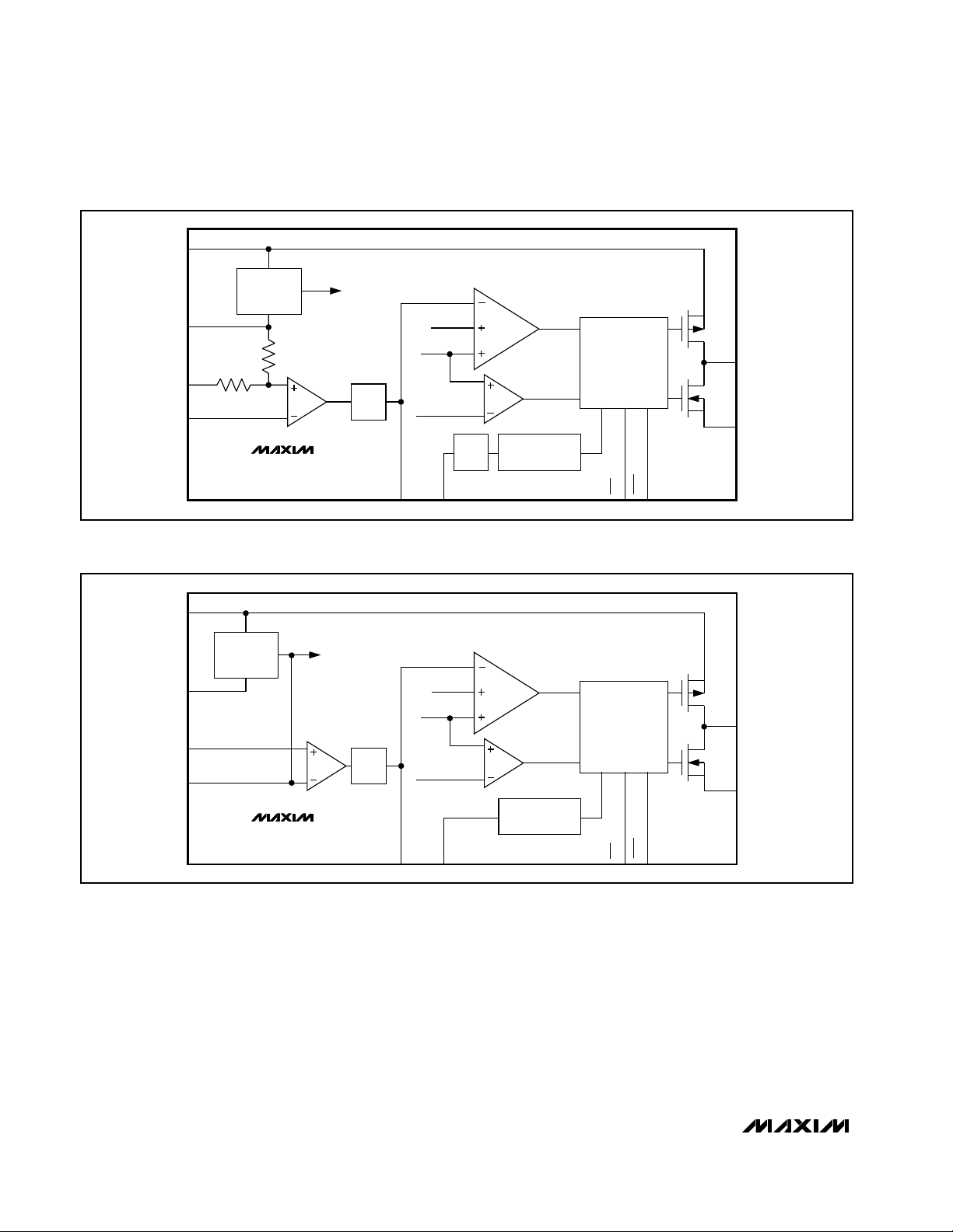
A new cycle begins at each falling edge of the internal
oscillator. The controller turns on the P-channel MOSFET to increase the inductor current, and the slope
compensation block initiates a new reference current
ramp that is summed with the internal P-channel MOSFET current (Figures 1 and 2).
The second half of the cycle begins when the reference
ramp is greater than the error voltage. The P-channel
MOSFET is turned off, the synchronous rectifier is
turned on, and inductor current continues to flow to the
output capacitor. The output capacitor stores charge
when the current is high and releases it when the
inductor current is low, smoothing the voltage across
Figure 1. MAX1820 Simplified Functional Diagram (No SYNC for MAX1820Z)
Figure 2. MAX1821 Simplified Functional Diagram (No SYNC for MAX1821)
BATT
TO
MAX1820
1.25V
IC BIAS
TRANSIMPEDANCE
ERROR AMP
CLAMP
ERROR SIGNAL
SLOPE COMP
CURRENT SENSE
0.45V TO 2.15V
SKIP THRESHOLD
÷13 OR
÷18
PWM
COMPARATOR
SKIP
COMPARATOR
1MHz
OSCILLATOR
GND
OUT
REF
VOLTAGE
REFERENCE
PWM CONTROL
AND
SKIP LOGIC
LX
PGND
SYNC
COMP
BATT
1.25V
TO
IC BIAS
TRANSIMPEDANCE
ERROR AMP
CLAMP
ERROR SIGNAL
SLOPE COMP
CURRENT SENSE
0.45V TO 2.15V
SKIP THRESHOLD
GND
OUT
REF
VOLTAGE
REFERENCE
MAX1821
SYNC
COMP
PWM
COMPARATOR
SKIP
COMPARATOR
1MHz
OSCILLATOR
SKIP
PWM CONTROL
AND
SKIP LOGIC
SKIP
SHDN
LX
PGND
SHDN
Page 11

MAX1820/MAX1821
WCDMA Cellular Phone 600mA
Buck Regulators
______________________________________________________________________________________ 11
the load. The duty cycle of a buck step-down converter
is ideally a ratio of the output voltage to input voltage in
steady-state condition.
The MAX1820/MAX1821 have internal switch current
limits of 1.2A (typ). If ILXexceeds this maximum, the
high-side FET turns off and the synchronous rectifier
turns on. This lowers the duty cycle and causes the output voltage to droop as long as the load current
remains excessive. There is also a synchronous rectifier
current limit of -0.85A when the device is operating in
forced PWM mode (see the Forced PWM Operation section). If the negative current limit is exceeded, the synchronus rectifier is turned off, and the inductor current
continues to flow through its body diode until the beginning of the next cycle or the inductor current drops to
zero. This means there is a limit on how much current
the device is allowed to shuttle in response to output
power reduction.
Normal Mode Operation
Connecting SKIP to GND enables MAX1820/MAX1821
normal operation (Figure 3). This allows automatic PWM
control at medium and heavy loads and skip mode at
light loads to improve efficiency and reduce quiescent
current to 180µA. Operating in normal mode also allows
the MAX1820/MAX1821 to pulse skip when the peak
inductor current drops below 130mA, corresponding to
a load current of approximately 65mA.
During skip operation, the MAX1820/MAX1821 switch
only as needed to service the load, reducing the
switching frequency and associated losses in the internal switch, the synchronous rectifier, and the external
inductor.
There are three steady-state operating conditions for
the MAX1820/MAX1821 in normal mode. The device
performs in continuous conduction for heavy loads in a
manner identical to forced PWM mode. The inductor
current becomes discontinuous at medium loads,
requiring the synchronous rectifier to be turned off
before the end of a cycle as the inductor current reaches zero. The device enters into skip mode when the
converter output voltage exceeds its regulation limit
before the inductor current reaches its skip threshold level.
During skip mode, a switching cycle initiates when the
output voltage has dropped out of regulation. The Pchannel MOSFET switch turns on and conducts current
to the output-filter capacitor and load until the inductor
current reaches the skip peak current limit. Then the
main switch turns off, and the magnetic field in the
inductor collapses, while current flows through the synchronous rectifier to the output filter capacitor and the
load. The synchronous rectifier is turned off when the
inductor current reaches zero. The MAX1820/ MAX1821
wait until the skip comparator senses a low output voltage again.
Forced PWM Operation
Connect SKIP to BATT for forced PWM operation.
Forced PWM operation is desirable in sensitive RF and
data-acquisition applications to ensure that switching
harmonics do not interfere with sensitive IF and datasampling frequencies. A minimum load is not required
during forced PWM operation since the synchronous
rectifier passes reverse-inductor current as needed to
allow constant-frequency operation with no load.
Figure 3. Standard Operating Circuit
= 2.6V TO 5.5V
V
IN
10µF 0.1µF
0.047µF
* CAN BE OMITTED IF CERAMIC OUTPUT CAPACITOR IS USED.
BATT
SHDN
SYNC
REF
SKIP GND
MAX1821
PGND
COMP
4.7µH
LX
4.7µF
FB
R
C
82kΩ
C1
330pF
C2*
1pF
V
= 1.5V
OUT
R1
6kΩ
R2
30kΩ
Page 12

MAX1820/MAX1821
WCDMA Cellular Phone 600mA
Buck Regulators
12 ______________________________________________________________________________________
Forced PWM operation uses higher supply current with
no load (3.3mA typ) compared to skip mode.
100% Duty-Cycle Operation
The on-time can exceed one internal oscillator cycle,
which permits operation up to 100% duty cycle. As the
input voltage drops, the duty cycle increases until the
P-channel MOSFET is held on continuously. Dropout
voltage in 100% duty cycle is the output current multiplied by the on-resistance of the internal switch and
inductor, approximately 150mV (I
OUT
= 600mA). Near
dropout, the on-time may exceed one PWM clock
cycle; therefore, small-amplitude subharmonic ripple
may occur.
COMP Clamp
The MAX1820/MAX1821 compensation network has a
0.45V to 2.15V error regulation range. The clamp prevents COMP from rising too high or falling too low to
optimize transient response.
Dropout
Dropout occurs when the input voltage is less than the
desired output voltage plus the IR drops in the circuit
components. The duty cycle is 100% during this condition, and the main switch remains on, continuously
delivering current to the output up to the current limit.
IR drops in the circuit are primarily caused by the onresistance of the main switch and the resistance in the
inductor.
During dropout, the high-side P-channel MOSFET turns
on, and the controller enters a low-current consumption
mode. Every 6µs (6 cycles), the MAX1820/MAX1821
check to see if the device is still in dropout. The device
remains in this mode until the MAX1820/MAX1821 are
no longer in dropout.
Undervoltage Lockout (UVLO)
The MAX1820/MAX1821 do not operate with battery
voltages below the UVLO threshold of 2.35V (typ). The
BATT input remains high impedance until the supply
voltage exceeds the UVLO threshold. This guarantees
the integrity of the output voltage regulation and prevents excessive current during startup and as the battery supply voltage drops during usage.
Synchronous Rectification
An N-channel synchronous rectifier eliminates the need
for an external Schottky diode and improves efficiency.
The synchronous rectifier turns on during the second
half of each cycle (off-time). During this time, the voltage across the inductor is reversed, and the inductor
current falls. In normal mode, the synchronous rectifier
is turned off when either the output falls out of regulation (and another on-time begins) or when the inductor
current approaches zero. In forced PWM mode, the
synchronous rectifier remains active until the beginning
of a new cycle.
SYNC Input and Frequency Control
The MAX1820Z and MAX1821 internal oscillator is set
to a fixed 1MHz switching frequency. The MAX1820Z
and MAX1821 do not have synchronizing capability
and the SYNC pin must be connected to GND. The
MAX1820Y, MAX1820X, and MAX1821X are capable of
synchronizing to external signals. For external synchronization, drive the SYNC pin with a 13MHz (MAX1820X
and MAX1821X) or 19.8MHz (MAX1820Y) AC-coupled
sine wave. SYNC has a perfect 13:1 (MAX1820X and
MAX1821X) or 18:1 (MAX1820Y) clock divider for 1MHz
(MAX1820X and MAX1821X) or 1.1MHz (MAX1820Y)
switching from common system clocks. The input frequency range for SYNC is 10MHz to 16MHz
(MAX1820X, MAX1821X) or 15MHz to 21MHz
(MAX1820Y). Connect SYNC to GND to use the internal
free-running oscillator at 1MHz.
Shutdown Mode
Drive SHDN to GND to place the MAX1820/MAX1821 in
shutdown mode. In shutdown, the reference, control
circuitry, internal switching MOSFET, and the synchronous rectifier turn off, reducing the supply current to
0.1µA, and the output goes high impedance. Connect
SHDN to BATT for normal operation.
Current-Sense Comparators
The MAX1820/MAX1821 use several internal currentsense comparators. In PWM operation, the PWM comparator terminates the cycle-by-cycle on-time (Figures
1 and 2) and provides improved load and line
response. This allows tighter specification of the inductor-saturation current limit to reduce inductor cost. A
second current-sense comparator used across the Pchannel switch controls entry into skip mode. A third
current-sense comparator monitors current through the
internal N-channel MOSFET to prevent excessive
reverse currents and determine when to turn off the
synchronous rectifier. A fourth comparator used at the
P-channel MOSFET detects overcurrent. This protects
the system, external components, and internal
MOSFETs under overload conditions.
Page 13
MAX1820/MAX1821
WCDMA Cellular Phone 600mA
Buck Regulators
______________________________________________________________________________________ 13
Applications Information
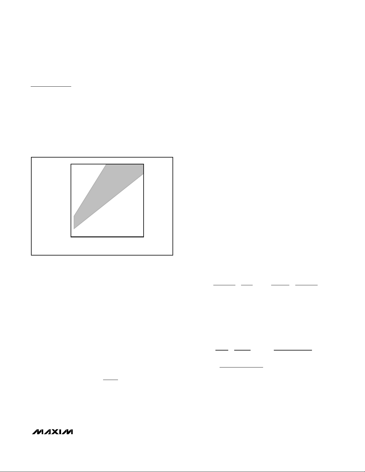
Setting the Output Voltage (MAX1820)
The MAX1820 is optimized for highest system efficiency
when applying power to a linear PA in WCDMA handsets. When transmitting at less than full power, the supply voltage to the PA is reduced (from 3.4V to as low as
0.4V) to greatly reduce battery current. Figure 4 shows
the typical WCDMA PA load profile. The use of a DCDC converter such as the MAX1820 dramatically
reduces battery drain in these applications.
The MAX1820’s output voltage is dynamically
adjustable from 0.4V to V
BATT
by the use of the REF
input. The gain from V
REF
to V
OUT
is internally set to
1.76. V
OUT
can be adjusted during operation by driving
REF with an external DAC. The MAX1820 output
responds to full-scale change in voltage and current in
<30µs.
Setting the Output Voltage (MAX1821)
The MAX1821 is intended for general-purpose stepdown applications where high efficiency is a priority.
Select an output voltage between 1.25V and V
BATT
by
connecting FB to a resistive divider between the output
and GND (Figure 3). Select feedback resistor R2 in the
5kΩ to 30kΩ range. R1 is then given by:
where V
FB
= 1.25V.
Compensation and Stability
The MAX1820/MAX1821 are externally compensated
by placing a resistor and a capacitor (RCand C1) in
series, from COMP to GND (Figure 3). The capacitor
integrates the current from the transimpedance amplifier, averaging output capacitor ripple. This sets the
device speed for transient responses and allows the
use of small ceramic output capacitors because the
phase-shifted capacitor ripple does not disturb the current regulation loop. The resistor sets the proportional
gain of the output error voltage by a factor g
m
✕
RC.
Increasing this resistor also increases the sensitivity of
the control loop to the output capacitor ripple.
This resistor and capacitor set a compensation zero
that defines the system’s transient response. The load
pole is a dynamic pole, shifting the pole frequency with
changes in load. As the load decreases, the pole frequency shifts to the left. System stability requires that
the compensation zero must be placed properly to
ensure adequate phase margin (at least 30° at unity
gain). The following is a design procedure for the compensation network:
1) Select an appropriate converter bandwidth (fC) to
stabilize the system while maximizing transient
response. This bandwidth should not exceed 1/5 of
the switching frequency. Use 100kHz as a reasonable starting point.
2) Calculate the compensation capacitor, C1, based
on this bandwidth:
Resistors R1 and R2 are internal to the MAX1820; use
R1 = 151kΩ and R2 = 199kΩ as nominal values for calculations. These resistors are external to the MAX1821
(see the Setting the Output Voltage section). Using
V
OMAX
= 3.4V, I
OMAX
= 0.6A, gm= 50µs, RCS= 0.75Ω,
C1 is evaluated as:
TION 3
Selecting the nearest standard value of 330pF corresponds to a 103kHz bandwidth, which is still acceptable per the above criteria.
Figure 4. Typical WCDMA PA Load Profile
3.4
3.0
1.0
WCDMA PA SUPPLY VOLTAGE (V)
0.4
30 600
WCDMA PA SUPPLY CURRENT (mA)
R1
=
300
R2 1
V
OUT
V
FB
-
C1
V
O(MAX)
=
I
O(MAX) CS
1
×
g
R
m
R1+R212
R2
××
π f
C
C1
3.4V
=
0.6A10
×
23
..75
Ω
1
××
14 100
50 s
kHz
×
µ
151k +199k
= 341pF
1
99
Ω
k
ΩΩ
Page 14

MAX1820/MAX1821
WCDMA Cellular Phone 600mA
Buck Regulators
14 ______________________________________________________________________________________
3) Calculate the equivalent load impedance, RL, by:
4) Calculate the compensation resistance (R
C
) value to
cancel out the dominant pole created by the output
load and the output capacitance:
Solving for R
C
gives:
5) Calculate the high-frequency compensation pole to
cancel the zero created by the output capacitor’s
equivalent series resistance (ESR):
Solving for C2 gives:
In this case, C2 can be omitted due to the use of
ceramic capacitors. Larger output capacitors and higher ESR may require the use of capacitor C2.
Inductor Selection
A 4µH to 6µH inductor with a saturation current of at
least 800mA is recommended for most applications.
For best efficiency, the inductor’s DC resistance should
be <200mΩ, and saturation current should be >1A. See
Table 1 for recommended inductors and manufacturers.
For most designs, a reasonable inductor value (L
IDEAL
)
can be derived from the following equation:
where LIR is the inductor current ripple as a percentage.
LIR should be kept between 20% and 40% of the maximum load current for best performance and stability.
The maximum inductor current is:
The inductor current becomes discontinuous if I
OUT
decreases to LIR/2 from the output current value used
to determine L
IDEAL
.
Input Capacitor Selection
The input capacitor reduces the current peaks drawn
from the battery or input power source and reduces
switching noise in the IC. The impedance of the input
capacitor at the switching frequency should be less
than that of the input source so high-frequency switching currents do not pass through the input source.
The input capacitor must meet the ripple-current
requirement (I
RMS
) imposed by the switching currents.
Nontantalum chemistries (ceramic, POSCAP, or OSCON) are preferred due to their resistance to power-up
surge currents:
For optimal circuit reliability, choose a capacitor that
has less than 10°C temperature rise at the peak ripple
current.
Table 1. Suggested Inductors
MANUFACTURER PART NUMBER
Coilcraft DO1606 4.7 120 1.2 5.3 ✕ 5.3 ✕ 2.0
Coilcraft LPT1606-472 4.7 240 (max) 1.2 6.5 ✕ 5.3 ✕ 2.0
Sumida CDRH4D18-4R7 4.7 125 0.84 5 ✕ 5 ✕ 2
Sumida CR43 4.7 108.7 1.15 4.5 ✕ 4.0 ✕ 3.5
Sumida CDRH5D18-4R1 4.1 57 1.95 5.5 ✕ 5.5 ✕ 2.0
×× ×
2
R
=
C
CF
R
×
L OUT
C1
V
OUT(MAX)
R
≈
L
I
OUT(MAX)
1
L OUT C
=
×× ×ππRC RC1
2
3.4V
=
0.6A
4.7
330
µ
pF
1
= 80.8k
INDUCTANCE
(µH)
Ω
ESR (mΩ)
SATURATION
CURRENT (A)
L
IDEAL
=
V(V -V)
OUT BATT OUT
×× ×ƒLIR I
V
BATT OUT(MAX) OSC
LIR
II
L(MAX) OUT(MAX)
=+
1
2
×× ×
2
1
ESR OUT
=
1
×× ×ππRC RC32
2
`
RC
C
×
ESR OUT
Rk
3
4.7 Fµ .
=
80 8
×
.
001
Ω
Ω
.
pF2
055=
=
I
RMS LOAD
V(V -V)
=
I
OUT BATT OUT
V
BATT
DIMENSIONS
(mm)
Page 15

MAX1820/MAX1821
WCDMA Cellular Phone 600mA
Buck Regulators
______________________________________________________________________________________ 15
Output Capacitor Selection
The output capacitor is required to keep the output voltage ripple small and to ensure regulation control loop
stability. The output capacitor must have low impedance at the switching frequency. Ceramic capacitors
are recommended. The output ripple is approximately:
V
RIPPLE
≈ LIR ✕I
OUT(MAX)
See the Compensation Design section for a discussion
of the influence of output capacitance and ESR on regulation control-loop stability.
The capacitor voltage rating must exceed the maximum
applied capacitor voltage. Consult the manufacturer’s
specifications for proper capacitor derating. Avoid Y5V
and Z5U dielectric types due to their huge voltage and
temperature coefficients of capacitance and ESR.
PC Board Layout and Routing
High switching frequencies and large peak currents
make PC board layout a very important part of design.
Good design minimizes excessive EMI on the feedback
paths and voltage gradients in the ground plane, both
of which can result in instability or regulation errors.
Connect the inductor, input filter capacitor, and output
filter capacitor as close together as possible, and keep
their traces short, direct, and wide. Connect their
ground pins at a single common node in a star-ground
configuration. The external voltage-feedback network
should be very close to the FB pin, within 0.2in (5mm).
Keep noisy traces (from the LX pin, for example) away
from the voltage-feedback network; also, keep them
separate, using grounded copper. Connect GND and
PGND at a single point, as close as possible to the
MAX1820/MAX1821. The MAX1820/MAX1821 evaluation kit manual illustrates an example PC board layout
and routing scheme.
UCSP Package Consideration
For general UCSP package information and PC layout
considerations, refer to the Maxim Application Note
(Wafer-Level Ultra-Chip-Board-Scale Package).
______________________UCSP Reliability
The chip-scale package (UCSP) represents a unique
packaging form factor that may not perform equally to a
packaged product through traditional mechanical reliability tests. UCSP reliability is integrally linked to the
user’s assembly methods, circuit board material, and
usage environment. The user should closely review
these areas when considering use of a UCSP package.
Performance through Operating Life Test and Moisture
Resistance remains uncompromised as it is primarily
determined by the wafer-fabrication process.
Mechanical stress performance is a greater consideration for a UCSP package. UCSPs are attached through
direct solder contact to the user’s PC board, foregoing
the inherent stress relief of a packaged-product lead
frame. Solder joint contact integrity must be considered. Information on Maxim’s qualification plan, test
data, and recommendations are detailed in the UCSP
application note, which can be found on Maxim’s website,
www.maxim-ic.com.
____________________Chip Information
TRANSISTOR COUNT: 2722
Table 2. Capacitor Selection
Table 3. Component Manufacturers
ESR
×+
1
2
׃ ×
()
OSC OUT
C
CAPACITOR
C
BATT
C
OUT
(MAX1820)
C
OUT
(MAX1821)
MANUFACTURER
Coilcraft 847-639-6400 www.coilcraft.com
Kemet 408-986-0424 www.kemet.com
Panasonic 847-468-5624 w w w .p anasoni c.com
Sumida 847-956-0666 www.sumida.com
Taiyo Yuden 408-573-4150 www.t-yuden.com
CAPACITOR
VALUE (µF)
4.7 to 10 <150 Ceramic
2.2 to 4.7 <50 Ceramic
4.7 to 10 <150 Ceramic
USA PHONE
NUMBER
ESR
(mΩ)
CAPACITOR
TYPE
WEBSITE
Page 16

MAX1820/MAX1821
WCDMA Cellular Phone 600mA
Buck Regulators
16 ______________________________________________________________________________________
Typical Operating Circuits (continued)
1
2
3
4
5
10
9
8
7
6
SYNC
BATT
LXREF
( ) ARE FOR MAX1821 ONLY.
OUT (FB)
COMP
SKIP
MAX1820
MAX1821
µMAX
TOP VIEW
PGNDGND
SHDN
COMP OUT (FB)
SYNC
BATT LX
UCSP
TOP VIEW AFTER ASSEMBLED ON PC BOARD (BUMPS AT THE BOTTOM)
( ) ARE FOR MAX1821 ONLY.
A1 A3A2
B1
C1 C2 C3
A
B
C
1
2
3
GND
PGND
A4
B4
C4
4
REFSKIP
SHDN
Pin Configurations
Ordering Information (continued)
*UCSP reliability is integrally linked to the user’s assembly methods, circuit board material, and environment. Refer to the UCSP
Reliability Notice in the UCSP Reliability section for more information.
✕
4 UCSP AAC
✕
4 UCSP AAV
PART
MAX1821EBC*
MAX1821EUB
MAX1821XEBC*
MAX1821XEUB
SYNC
FREQ (MHz)
No Sync
No Sync
13
13
OUTPUT VOLTAGE TEMP RANGE PIN-PACKAGE UCSP MARK
Programmable -40°C to +85°C3
Programmable -40°C to +85°C 10 µMAX —
Programmable -40°C to +85°C3
Programmable -40°C to +85°C10 µMAX —
INPUT
2.6V TO
5.5V
BATT
SHDN
SYNC
REF
SKIP
LX
PGND
FB
MAX1821
COMP
GND
OUTPUT
1.25V TO 5.5V
Page 17

MAX1820/MAX1821
WCDMA Cellular Phone 600mA
Buck Regulators
______________________________________________________________________________________ 17
Package Information
(The package drawing(s) in this data sheet may not reflect the most current specifications. For the latest package outline information,
go to www.maxim-ic.com/packages.)
12L, USPC.EPS
Page 18

MAX1820/MAX1821
WCDMA Cellular Phone 600mA
Buck Regulators
Maxim cannot assume responsibility for use of any circuitry other than circuitry entirely embodied in a Maxim product. No circuit patent licenses are
implied. Maxim reserves the right to change the circuitry and specifications without notice at any time.
18 ____________________Maxim Integrated Products, 120 San Gabriel Drive, Sunnyvale, CA 94086 408-737-7600
© 2002 Maxim Integrated Products Printed USA is a registered trademark of Maxim Integrated Products.
Package Information (continued)
(The package drawing(s) in this data sheet may not reflect the most current specifications. For the latest package outline information,
go to www.maxim-ic.com/packages.)
10LUMAX EPS
e
10
ÿ 0.50±0.1
0.6±0.1
1
0.6±0.1
TOP VIEW
4X S
H
BOTTOM VIEW
10
DIM
A1
A2 0.030 0.037 0.75 0.95
D1
D2
E1
E2
H
L
L1
1
b
e
S
α
INCHES
MAX
MIN
-A
0.043
0.006
0.002
0.116
0.120
0.114
0.118
0.116
0.120
0.114
0.118
0.187
0.0157
0.007
0.0035
c
0.199
0.0275
0.037 REF
0.0106
0.0197 BSC
0.0078
0.0196 REF
6∞
0∞ 0∞ 6∞
MILLIMETERS
MAX
MIN
-
1.10
0.15
0.05
3.05
2.95
2.89
3.00
2.95
3.05
2.89
3.00
4.75
5.05
0.40
0.70
0.940 REF
0.177
0.270
0.500 BSC
0.090
0.200
0.498 REF
D2
A2
b
D1
A
A1
GAGE PLANE
α
FRONT VIEW
E2
E1
SIDE VIEW
c
L
L1
PROPRIETARY INFORMATION
TITLE:
PACKAGE OUTLINE, 10L uMAX/uSOP
REV.DOCUMENT CONTROL NO.APPROVAL
21-0061
1
I
1
 Loading...