

Page 1

General Description
The MAX1817 is a compact, high-efficiency, dual-output step-up converter for portable devices that provides both the main logic supply and the LCD bias. The
device operates from an input voltage of +1.5V to
+5.5V, allowing the use of 2- or 3-cell alkaline batteries,
or 1-cell lithium-ion (Li+) batteries.
The MAX1817’s main regulator supplies 125mA at
either a preset 3.3V or an adjustable 2.5V to 5.5V output voltage with up to 88% efficiency. A 0.1µA shutdown state also minimizes battery drain. The
MAX1817’s secondary step-up converter provides the
LCD bias voltage and is adjustable up to +28V.
Other features include a fast switching frequency to
reduce the size of external components and a low quiescent current to maximize battery life. Both outputs can
be independently shut down for improved flexibility.
The MAX1817 is supplied in a compact 10-pin µMAX
package. The MAX1817 evaluation kit (MAX1817EVKIT)
is available to speed up design.
________________________Applications
Organizers/Translators
PDAs
MP3 Players
GPS Receivers
Features
♦ Dual Step-Up Converter in a Tiny 10-Pin µMAX
Package
♦ Main Output
Up to 125mA Load Current
Fixed 3.3V or Adjustable 2.5V to 5.5V
Up to 88% Efficiency
Internal Switch
♦ LCD Output
Up to 28V for LCD Bias
Internal Switch
♦ Input Voltage Range +1.5V to +5.5V
♦ Minimal External Components Required
♦ 0.1µA Logic-Controlled Shutdown
♦ Low 15µA Quiescent Supply Current
MAX1817
Compact, High-Efficiency, Dual-Output
Step-Up DC-DC Converter
________________________________________________________________ Maxim Integrated Products 1
Pin Configuration
MAX1817
LX
ONLCD
ON
FB
OUT
FBLCDLCD ON/OFF
+1.5V
TO +5.5V
MAIN ON/OFF MAIN
LCD
AGND GND
LXLCD
Typical Operating Circuit
19-1794 Rev 0; 10/00
Ordering Information
For price, delivery, and to place orders, please contact Maxim Distribution at 1-888-629-4642,
or visit Maxim’s website at www.maxim-ic.com.
PART
MAX1817EUB -40°C to +85°C 10 µMAX
TEMP. RANGE
PIN-PACKAGE
TOP VIEW
ONLCD
1
FB
2
ON
MAX1817
3
4
5
MAX
µ
10
OUT
9
LX
8
GND
7
LXLCDFBLCD
N.C.AGND
6
Page 2

MAX1817
Compact, High-Efficiency, Dual-Output
Step-Up DC-DC Converter
2 _______________________________________________________________________________________
ABSOLUTE MAXIMUM RATINGS
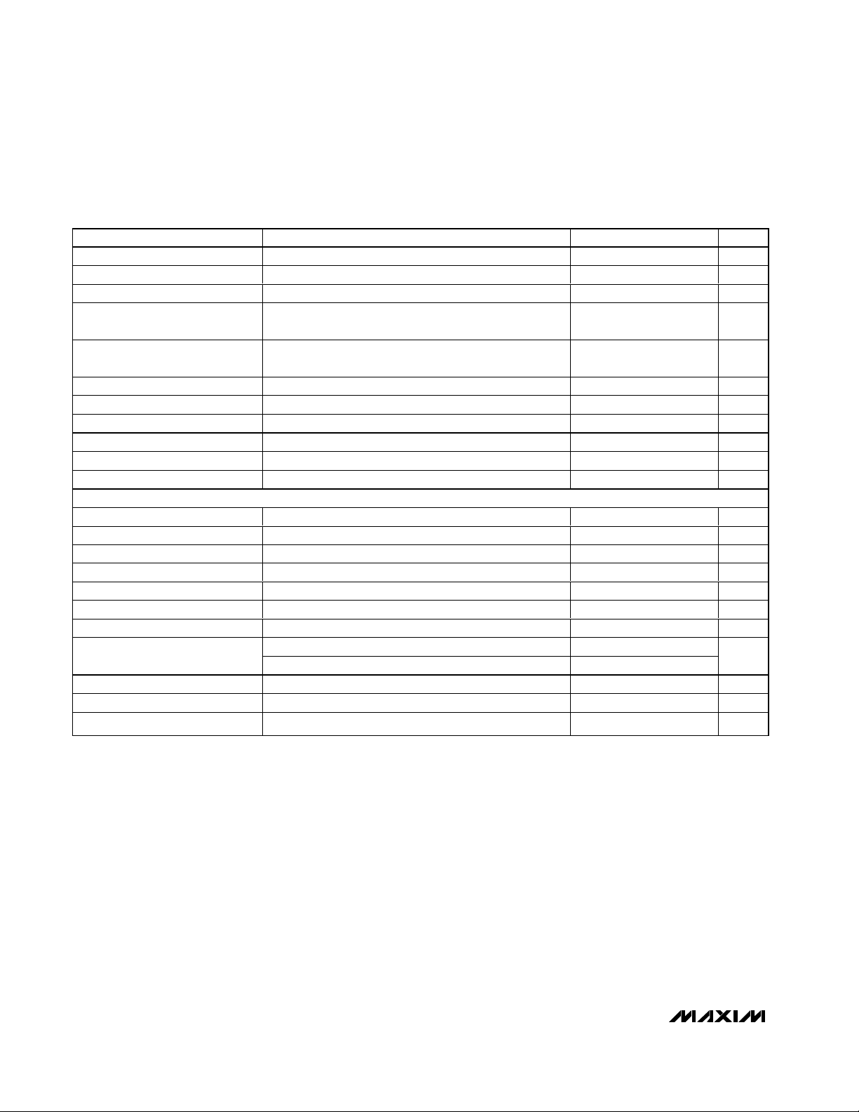
ELECTRICAL CHARACTERISTICS
(VON= V
ONLCD =VOUT
= +3.3V, FB = GND, TA= 0°C to +85°C, unless otherwise noted. Typical values are at TA= +25°C.)
Stresses beyond those listed under “Absolute Maximum Ratings” may cause permanent damage to the device. These are stress ratings only, and functional
operation of the device at these or any other conditions beyond those indicated in the operational sections of the specifications is not implied. Exposure to
absolute maximum rating conditions for extended periods may affect device reliability.
OUT to GND .............................................................-0.3V to +6V
ON, ONLCD, FB, FBLCD, LX to GND ......-0.3V to (V
OUT
+ 0.3V)
LXLCD to GND .......................................................-0.3V to +30V
AGND to GND .......................................................-0.3V to +0.3V
Continuous Power Dissipation (T
A
= +70°C)
10-Pin µMAX (derate 5.6mW/°C above +70°C) ...........444mW
LXLCD, LX Maximum Current ........................................0.5A
RMS
Operating Temperature Range ...........................-40°C to +85°C
Junction Temperature......................................................+150°C
Storage Temperature Range .............................-65°C to +150°C
Lead Temperature (soldering, 10s) .................................+300°C
Dual Mode is a trademark of Maxim Integrated Products.
PARAMETER CONDITIONS MIN TYP MAX UNITS
GENERAL
Input Voltage Range 1.5 5.5 V
Startup Voltage
Quiescent Current from OUT
(Main Only)
Quiescent Current from OUT VFB = V
Shutdown Quiescent Current VON = V
MAIN OUTPUT
OUT Undervoltage Lockout
Fixed-Mode Output Voltage VFB ≤ 45mV 3.14 3.3 3.47 V
Adjustable-Mode FB Regulation
Voltage
FB Input Bias Current VFB = 1.35V 50 nA
FB Dual Mode
Output Voltage Adjustment
Range
Maximum LX On-Time VFB = 0.5V 2.4 5 7.5 µs
Zero Crossing Comparator
Threshold (V
Zero Crossing Comparator
Backup Timer
Line Regulation
Load Regulation
LX On-Resistance V
LX Current Limit 0.5 0.75 1.05 A
TM
LX
R
= 35Ω 1.5
LOAD
= ∞, VFB = 1.35V 1.2 1.55
R
LOAD
VFB = V
V
ONLCD
V
rising, VFB = 1.35V 2.2 2.4
OUT
falling, V
V
OUT
Threshold 45 75 105 mV
- V
)
OUT
= +0.5V 22 45 70 µs
V
FB
I
= 100mA,
OUT
= +2V to +3V
V
IN
V
= +2.5V,
IN
= 10mA to 100mA
I
LOAD
= 3.3V, ILX = 100mA 0.35 0.65 Ω
OUT
= 1.35V,
FBLCD
= 0
= 1.35V 15 30 µA
FBLCD
= 0 0.1 1 µA
ONLCD
= 1.35V 1.95 2.15
FB
510µA
1.20 1.25 1.30 V
2.5 5.5 V
02040mV
1.6 %
1.6 %
V
V
Page 3

MAX1817
Compact, High-Efficiency, Dual-Output
Step-Up DC-DC Converter
_______________________________________________________________________________________ 3
ELECTRICAL CHARACTERISTICS (continued)
(VON= V
ONLCD
= V
OUT
= +3.3V, FB = GND, TA= 0°C to +85°C, unless otherwise noted. Typical values are at TA= +25°C.)
ELECTRICAL CHARACTERISTICS
(VON= V
ONLCD
= V
OUT
= +3.3V, FB = GND, TA= -40°C to +85°C, unless otherwise noted.) (Note 1)
LX Leakage Current VON = GND, VLX = 5.5V 0.1 1 µA
ON Input Low Voltage 1.8V < V
ON Input High Voltage 1.8V < V
ON Input Bias Current 1µA
LCD OUTPUT
LXLCD Voltage 28 V
LXLCD On-Resistance V
LXLCD Current Limit 0.28 0.5 0.7 A
LXLCD Leakage Current V
FBLCD Regulation Voltage 1.20 1.25 1.30 V
FBLCD Input Bias Current V
LCD Line Regulation I
LCD Load Regulation I
Maximum LXLCD On-Time 4 9 14 µs
Minimum LXLCD Off-Time
ONLCD Input Low Voltage 2.5V < V
ONLCD Input High Voltage 2.5V < V
ONLCD Input Bias Current 1µA
PARAMETER CONDITIONS MIN TYP MAX UNITS
< 5.5V, VFB = 0.5V 400 mV
OUT
< 5.5V, VFB = 0.5V 1.6 V
OUT
= 3.3V, I
OUT
= 28V, V
LXLCD
= 1.35V 50 nA
FBLCD
= 5mA, VIN = +2V to +3V 0.1 %
LOAD
= 1mA to 5mA, VIN = +2.5V 0.5 %
LOAD
V
≥ 1.2V 0.5 1 1.5
FBLCD
V
≤ 0.7V 2.4 5 7.5
FBLCD
OUT
OUT
= 100mA 1.1 2.0 Ω
LXLCD
= 0 0.1 1 µA
ONLCD
< 5.5V 400 mV
< 5.5V 1.6 V
µs
GENERAL
Input Voltage Range 1.5 5.5 V
Startup Voltage R
Quiescent Current from OUT
(Main Only)
Quiescent Current from OUT VFB = V
Shutdown Quiescent Current VON = V
MAIN OUTPUT
OUT Undervoltage Lockout
Fixed-Mode Output Voltage VFB ≤ 45mV 3.14 3.47 V
Adjustable-Mode FB Regulation
Voltage
FB Input Bias Current VFB = 1.35V 50 nA
PARAMETER CONDITIONS MIN MAX UNITS
= ∞, VFB = 1.35V 1.7 V
LOAD
V
= V
FB
V
rising, VFB = 1.35V 2.4
OUT
falling, VFB = 1.35V 1.95
V
OUT
= 1.35V, V
FBLCD
= 1.35V 30 µA
FBLCD
= 0 1 µA
ONLCD
= 0 10 µA
ONLCD
1.20 1.30 V
V
Page 4
MAX1817
Compact, High-Efficiency, Dual-Output
Step-Up DC-DC Converter
4 _______________________________________________________________________________________
ELECTRICAL CHARACTERISTICS (continued)
(VON= V
ONLCD
= V
OUT
= +3.3V, FB = GND, TA= -40°C to +85°C, unless otherwise noted.) (Note 1)
Note 1: Specifications to -40°C are guaranteed by design and not production tested.
FB Dual Mode Threshold 45 105 mV
Outp ut V ol tag e Ad j ustm ent Rang e 2.5 5.5 V
Maximum LX On-Time VFB = 0.5V 2.4 7.5 µs
Zero Crossing Comparator
Threshold (V
Zero Crossing Comparator
Backup Timer
LX On-Resistance V
LX Current Limit 0.42 1.05 A
LX Leakage Current VON = GND, VLX = 5.5V 1 µA
ON Input Low Voltage 1.8V < V
ON Input High Voltage 1.8V < V
ON Input Bias Current 1µA
LCD OUTPUT
LXLCD Voltage 28 V
LXLCD On-Resistance V
LXLCD Current Limit 0.25 0.7 A
LXLCD Leakage Current V
FBLCD Regulation Voltage 1.20 1.30 V
FBLCD Input Bias Current V
Maximum LXLCD On-Time 4 14 µs
Minimum LXLCD Off-Time
ONLCD Input Low Voltage 2.5V < V
ONLCD Input High Voltage 2.5V < V
ONLCD Input Bias Current 1µA
PARAMETER CONDITIONS MIN MAX UNITS
LX
- V
)
OUT
V
= 0.5V 22 70 µs
FB
= 3.3V, ILX = 100mA 0.65 Ω
OUT
< 5.5V, VFB = 0.5V 400 mV
OUT
< 5.5V, VFB = 0.5V 1.6 V
OUT
= 3.3V, I
OUT
= 28V, V
LXLCD
= 1.35V 70 nA
FBLCD
V
≥ 1.2V 0.5 1.5
FBLCD
V
≤ 0.7V 2.2 7.5
FBLCD
OUT
OUT
= 100mA 2 Ω
LXLCD
= 0 1 µA
ONLCD
< 5.5V 400 mV
< 5.5V 1.6 V
040mV
µs
Page 5

MAX1817
Compact, High-Efficiency, Dual-Output
Step-Up DC-DC Converter
_______________________________________________________________________________________ 5
Typical Operating Characteristics
(Circuit of Figure 3, TA = +25°C, unless otherwise noted.)
MAIN OUTPUT EFFICIENCY
vs. LOAD CURRENT
MAX1817-01
75
70
65
60
55
50
45
EFFICIENCY (%)
40
35
30
25
0.01 0.1 1 10 100
95
A: VIN = 3.3V,
90
= 5V
V
OUT
85
80
EFFICIENCY (%)
75
70
0.1 10
B: VIN = 2.4V,
= 5V
V
OUT
C: VIN = 2.4V,
= 3.3V
V
OUT
E: VIN = 1.8V,
V
OUT
CIRCUIT OF FIGURE 2
1
LOAD CURRENT (mA)
D: VIN = 1.8V,
V
OUT
= 3.3V
100 1000
= 5V
NO-LOAD SUPPLY CURRENT
vs. INPUT VOLTAGE (LCD OFF)
18
16
14
12
10
8
6
SUPPLY CURRENT (µA)
4
2
0
1.0 2.01.5 2.5 3.0 3.5 4.0
INPUT VOLTAGE (V)
MAIN CONVERTER
SWITCHING WAVEFORM
MAX1817-06
LCD OUTPUT EFFICIENCY
vs. LOAD CURRENT
A: VIN = +2.4V, V
= +2.4V, V
B: V
IN
C: V
= +2.4V, V
IN
= +1.8V, V
D: V
IN
= +1.8V, V
E: V
IN
= +1.8V, V
F: V
IN
LOAD CURRENT (mA)
MAX1817 toc04
C
E
F
= 12V
LCD
= 18V
LCD
= 24V
LCD
= 12V
LCD
= 18V
LCD
= 24V
LCD
V
= 3.3V,
OUT
NO LOAD
STARTUP VOLTAGE vs. LOAD CURRENT
160
A
B
MAX1817-02
D
RESISTIVE LOAD
140
LCD OFF
120
100
80
60
LOAD CURRENT (mA)
40
20
0
1.0 1.21.1 1.3 1.4 1.5 1.6 1.7
STARTUP VOLTAGE (V)
NO-LOAD SUPPLY CURRENT
vs. INPUT VOLTAGE
450
400
350
300
250
200
150
SUPPLY CURRENT (µA)
100
50
0
021 3456
INPUT VOLTAGE (V)
V
OUT
= 18V, NO LOAD
V
LCD
R1 = 1MΩ, R2 = 75k
LCD CONVERTER
SWITCHING WAVEFORM
= 3.3V
MAX1817-07
MAX1817 toc03
MAX1817-05
Ω
A
B
C
0
0
A: ILX, 500mA/div
, 50mV/div, AC-COUPLED
B: V
OUT
, 5V/div
C: V
LX
V
= 2.4V, V
IN
OUT
= 3.3V, I
10µs/div
LOAD,OUT
= 50mA, V
ONLCD
= 0
A
0
B
C
0
A: I
, 500mA/div
LXLCD
, 100mV/div, AC-COUPLED
B: V
LCD
C: V
LXLCD
= 2.4V, V
V
IN
= 18V, I
V
LCD
, 10V/div
OUT
LOAD,LCD
4µs/div
= 3.3V, I
= 5mA
LOAD,OUT
= 0,
Page 6

MAX1817
Compact, High-Efficiency, Dual-Output
Step-Up DC-DC Converter
6 _______________________________________________________________________________________
Typical Operating Characteristics (continued)
(Circuit of Figure 3, TA= +25°C, unless otherwise specified)
400µs/div
MAIN LOAD TRANSIENT RESPONSE
MAX1817-08
A: V
OUT
, 100mV/div, AC-COUPLED
B: I
LOAD, OUT
, 50mA/div
V
IN
= 2.4V, V
OUT
= 3.3V
A
B
0
200µs/div
LCD LOAD TRANSIENT RESPONSE
MAX1817-09
A: V
LCD
, 50mV/div, AC-COUPLED
B: I
LOAD, OUT
, 10mA/div
V
IN
= 2.4V, V
OUT
= 3.3V (NO LOAD), V
LCD
= 18V
A
B
0
400µs/div
MAIN LINE TRANSIENT RESPONSE
MAX1817-10
A: V
OUT,
100mV/div, AC-COUPLED
B: V
IN,
1V/div
V
OUT
= 3.3V, I
LOAD,MAIN
= 20mA, V
ONLCD
= 0
A
B
2.4V
1.8V
200µs/div
LCD LINE TRANSIENT RESPONSE
MAX1817-11
A: V
LCD
, 100mV/div, AC-COUPLED
B: V
IN,
1V/div
V
OUT
= 3.3V (NO LOAD), V
LCD
= 18V, I
LOAD,LCD
= 2mA
A
B
2.4V
1.8V
100µs/div
MAIN OUTPUT TURN-ON/TURN-OFF
RESPONSE
MAX1817-12
A: V
OUT
, 2V/div
B: I
IN,
500mA/div
C: V
ON
, 5V/div
V
IN
= 2.4V, R
LOAD,MAIN
= 165Ω, V
ONLCD
= 0
A
B
0
0
0
C
400µs/div
LCD OUTPUT TURN-ON/TURN-OFF
RESPONSE
MAX1817-13
A: V
LCD
, 10V/div
B: I
IN,
200mA/div
C: V
ONLCD
, 5V/div
V
= 2.4V, V
= 3.3V (NO LOAD), R
= 9kΩ
A
B
0
0
0
C
Page 7

________________Detailed Description
The MAX1817 dual step-up converter is designed to
supply the main power and LCD bias for low-power,
hand-held devices. The MAX1817’s main step-up converter includes a 0.35Ω N-channel power MOSFET
switch and provides a fixed 3.3V or adjustable 2.5V to
5.5V output at up to 125mA from an input as low as
1.5V. The MAX1817’s LCD bias step-up converter
includes a high-voltage 1.1Ω power MOSFET switch to
support as much as 5mA at 28V (Figure 1). During
startup, the MAX1817 extends the LCD MOSFET switch
minimum off-time, limiting surge current. Both converters require an inductor and external rectifier.
The MAX1817 runs in bootstrap mode, powering the IC
from the main step-up converter’s output. Independent
logic-controlled shutdown for the main and LCD stepup converters reduces quiescent current to 0.1µA.
Main Step-Up Converter
The MAX1817 main step-up converter runs from a
+1.5V to +5.5V input voltage and produces a fixed 3.3V
or adjustable 2.5V to 5.5V output voltage as well as
biasing the internal control circuitry. The MAX1817
switches only as often as is required to supply sufficient
power to the load. This allows the converter to operate
at lower frequencies at light loads, improving efficiency.
The control scheme maintains regulation when the error
amplifier senses the output voltage is below the feedback threshold, turning on the internal N-channel MOSFET and initiating an on-time. The on-time is terminated
when the 0.75A current limit is reached or when the
maximum on-time is reached. The N-channel MOSFET
remains off until the inductor current drops to 0, forcing
discontinuous inductor current. At the end of a cycle,
the error comparator waits for the voltage at FB to drop
below the regulation threshold, at which time another
cycle is initiated.
The main step-up converter uses a startup oscillator to
allow it to start from an input voltage as low as +1.2V.
This is necessary since the control circuitry is powered
from the step-up converter output (OUT). When the
voltage at OUT is below the OUT undervoltage lockout,
a fixed 50% duty cycle drives the internal N-channel
MOSFET, forcing the main output voltage to rise. Once
MAX1817
Compact, High-Efficiency, Dual-Output
Step-Up DC-DC Converter
_______________________________________________________________________________________ 7
Pin Description
PIN NAME FUNCTION
Main Output Feedback Input. Connect FB to GND for fixed 3.3V main output. For other output
1FB
2ON
3 ONLCD
4 FBLCD
5 AGND Analog Ground. Connect AGND to GND as close to the IC as possible.
6 N.C. No Connection. Not internally connected.
7 LXLCD
8 GND Power Ground. Connect GND to AGND as close to the IC as possible.
9LX
10 OUT
voltages, use a resistive voltage-divider to set the output voltage. The feedback regulation voltage
is 1.25V at FB.
Main Step-Up Converter On/Off Control. Connect ON to OUT for automatic startup. Connect ON to
GND to put the IC into shutdown mode.
LCD Output On/Off Control. Connect ONLCD to OUT to enable the LCD output. Connect ONLCD
to GND to disable the LCD output. The main output must be ≥2.4V to enable the LCD output.
LCD Output Feedback Input. Use a resistive voltage-divider from the LCD output to FBLCD to set
the voltage. The feedback regulation voltage is 1.25V at FBLCD.
LCD Output Switching Node. Drain of the internal N-channel MOSFET that drives the LCD output.
Connect an external inductor and rectifier to LXLCD.
Main Output Switching Node. Drain of the internal N-channel MOSFET that drives the main output.
Connect an external inductor and rectifier to LX.
Main Step-Up Converter Output. OUT is used to measure the output voltage in fixed mode (FB =
GND) and is the internal bias supply input to the IC. When shut down (ON = ONLCD = GND), OUT
is high impedance, drawing 1µA (max).
Page 8

MAX1817
the output voltage rises above the undervoltage threshold, the control circuitry is enabled, allowing proper
regulation of the output voltage.
LCD Step-Up Converter
The MAX1817’s LCD step-up converter generates an
LCD bias voltage up to 28V by use of a 500mA, 1.1Ω
internal N-channel switching MOSFET (Figure 1). The
LCD step-up converter control circuitry is powered from
the main step-up converter output (OUT), so the voltage
at OUT must be above the OUT undervoltage lockout
voltage for the LCD step-up converter to operate.
During startup, the MAX1817 extends the minimum offtime to 5µs for V
FBLCD
voltages <0.9V, limiting initial
surge current. The LCD step-up converter features an
independent shutdown control, ONLCD.
The LCD step-up converter features a minimum-offtime, current-limited control scheme. A pair of oneshots that set a minimum off-time and a maximum ontime governs the duty cycle. The switching frequency
can be up to 500kHz and depends upon the load, and
input and output voltages.
Compact, High-Efficiency, Dual-Output
Step-Up DC-DC Converter
8 _______________________________________________________________________________________
Figure 1. MAX1817 Simplified Functional Diagram
V
IN
FB
ON
ON
ON
OFF
ONLCD
OFF
75mV
SHUTDOWN
LOGIC
MAIN
SHUTDOWN
LOGIC
LCD
MAX1817
DUAL-MODE FEEDBACK
UNDERVOLTAGE
LOCKOUT
1.25V
1.25V
AGND
AGND
ERROR
COMPARATOR
MAIN
AGND
STARTUP
BIAS
LCD
ERROR
COMPARATOR
LCD
GND
ZEROCROSSING
DETECTOR
CONTROL
LOGIC
MAIN
CURRENT
LIMIT
MAIN
CONTROL
LOGIC
LCD
CURRENT
LIMIT
LCD
GND
GND
OUT
LXLCD
FBLCD
LX
MAIN
LCD
Page 9

Low-Voltage Startup
The MAX1817’s internal circuitry is powered from OUT.
The main step-up converter has a low-voltage startup
circuit to control main DC-DC converter operation until
V
OUT
exceeds the 2.2V (typ) undervoltage lockout
threshold. The minimum startup voltage is a function of
load current (see Typical Operating Characteristics).
The MAX1817 main converter typically starts up into a
35Ω load with input voltages down to +1.5V, allowing
startup with two alkaline cells even in deep discharge.
Shutdown: ON and ONLCD
The MAX1817 features independent shutdown control
of the main and LCD step-up converters. With both
converters shut down, supply current is reduced to
0.1µA. A logic low at ON shuts down the main step-up
converter, and LX enters a high-impedance state.
However, the main output remains connected to the
input through the inductor and output rectifier, holding
V
OUT
to one diode drop below the input voltage when
the main converter is shut down. If the input voltage is
sufficiently high to drive V
OUT
above the undervoltage
lockout voltage, the LCD step-up converter operates.
A logic low at ONLCD shuts down the LCD step-up
converter, and LXLCD enters a high-impedance state.
The LCD output remains connected to the input
through the inductor and output rectifier, holding it to
one diode drop below the input.
___________________Design Procedure
Setting the Main Output Voltage
The main step-up converter feedback input (FB) features Dual Mode operation. With FB grounded, the
main output voltage is preset to 3.3V. It can also be
adjusted from 2.5V to 5.5V with external resistors R3
and R4 as shown in Figure 2. To set the output voltage
externally, select resistor R4 from 10kΩ to 100kΩ.
Calculate R3 using:
R3 = R4 [(V
OUT
/ VFB) – 1]
where V
FB
= 1.25V, and V
OUT
can range from 2.5V to
5.5V.
Setting the LCD Output Voltage
Set the LCD output voltage with two external resistors
R1 and R2 as shown in Figure 3. Since the input leakage current at FBLCD has a maximum of 50nA, large
resistors can be used without significant accuracy loss.
Begin by selecting R2 in the 10kΩ to 100kΩ range, and
calculate R1 using the following equation:
R1 = R2 [(V
LCD
/ V
FBLCD
) – 1]
where V
FBLCD
= 1.25V, and V
LCD
can range from V
IN
to 28V.
MAX1817
Compact, High-Efficiency, Dual-Output
Step-Up DC-DC Converter
_______________________________________________________________________________________ 9
Figure 2. Setting Main Output Voltage Using External Resistors Figure 3. Typical Application Circuit
OFF
OFF
LCD
MAIN
ON
ON
C1
10µF
L2
10µH
LX
ONLCD
MAX1817
ON
AGND GND
L1
10µH
LXLCD
FBLCD
OUT
V
IN
D1
D2
4.7pF
C4
R3
300k
FB
R4
100k
C3
22µF
R1
1M
R2 75k
MAIN 5V
C2
1µF
LCD
18V
OFF
OFF
MAIN
V
IN
LCD
C1
10µF
ON
ONLCD
ON
ON
AGND GND
L2
10µH
LX
MAX1817
L1
10µH
D2
LXLCD
FBLCD
OUT
FB
D1
LCD 18V
C2
4.7pF
C4
C3
22µF
R1
1M
R2 75k
MAIN 3.3V
1µF
Page 10

MAX1817
Using a Charge Pump to Make Negative
LCD Output Voltage
The MAX1817 can generate a negative LCD output by
adding a diode-capacitor charge-pump circuit (D3, D4,
and C6) to the LXLCD pin as shown in Figure 4. FBLCD
is driven through a resistive voltage-divider from the
positive output, which is not loaded, allowing a very
small capacitor value at C2. For best stability and lowest ripple, the time constant of the R1 + R2 series combination and C2 should be near that of C5 and the
effective load resistance. Output load regulation of the
negative output degrades compared to the standard
positive output circuit and may rise at very light loads. If
this is not acceptable, reduce the resistance of R1 and
R2, while maintaining their ratio, to effectively preload
the output with a few hundred µA. This is why the R1
and R2 values shown in Figure 4 are lower than typical
values for a positive-output design. When loaded, the
magnitude of the negative output voltage is slightly
lower (closer to ground by approximately a diode forward voltage) than the voltage on C2.
Applications Information
Inductor Selection
The MAX1817’s high switching frequency allows the
use of small surface-mount inductors. The 10µH values
shown in Figure 3 are recommended for most applications, although values between 4.7µH and 47µH are
suitable. Smaller inductance values typically offer a
smaller physical size for a given series resistance,
allowing the smallest overall circuit dimensions. Larger
inductance values exhibit higher output current capability, but larger physical dimensions.
Circuits using larger inductance values may start up at
lower input voltages and exhibit less ripple, but they
may provide reduced output power. This occurs when
the inductance is sufficiently large to prevent the maximum current limit from being reached before the maximum on-time expires. The inductor’s saturation current
rating should be greater than the peak switching current. However, it is generally acceptable to bias most
inductors into saturation by as much as 20%, although
this may slightly reduce efficiency.
For best efficiency, select inductors with resistance no
greater than the internal N-channel FET resistance in
each step-up converter.
For maximum output current, choose L such that:
L < [(V
IN
✕
tON) / I
PEAK
]
where tONis the maximum switch on-time (5µs for main
step-up converter) or 9µs for LCD step-up converter)
and I
PEAK
is the switch peak current limit (0.75A for the
main step-up converter, or 0.5A for the LCD step-up
converter). With this inductor value, the maximum output
current the main converter is able to deliver is given by:
I
OUT(MAX)
= 0.5 ✕I
PEAK
/ (1 + tON/ t
OFF
)
where tON/ t
OFF
= (V
OUT
+ VD- VIN) / (VIN- VON), V
IN
and V
OUT
are the input and output voltages, VDis the
Schottky diode drop (0.3V typ), and VON= I
PEAK
✕
RON, where RONis the switch on-resistance.
For V
IN
= 1.5V and V
OUT
= 3.3V, with a minimum I
PEAK
value of 0.5A, and V
ON(MAX)
given by (0.5) ✕ (0.65) =
0.325V, the available output current that the converter
can provide is at least 90mA.
For larger inductor values, I
PEAK
is determined by:
I
PEAK
= [(V
IN
✕
tON) / L]
External Rectifiers
The high maximum switching frequency of the
MAX1817 requires a high-speed rectifier. Schottky
diodes such as the Motorola MBR0530 or the Nihon
EP05Q03L are recommended. To maintain high efficiency, the average current rating of the Schottky diode
should be greater than the peak switching current. A
junction diode such as the Central Semiconductor
CMPD4448 can be used for the LCD output with little
Compact, High-Efficiency, Dual-Output
Step-Up DC-DC Converter
10 ______________________________________________________________________________________
Figure 4. Negative Voltage for LCD Bias
C6
R3
L1,10µH
V
IN
C1
10µF
LX
L2
10µH
LXLCD
MAX1817
ONLCD
FBLCD
ON
AGND GND
OUT
FB
D2
0.1µF
1
D1**
C3
22µF
MAIN
C4
10pF
16.5k
R1
240k
*D3, D4 = CENTRAL SEMICONDUCTOR
CMPD7000 DUAL
**D1 = CENTRAL SEMICONDUCTOR
CMSD4448 (1N4148)
D4*
D3*
-19V
V
C5
1µF
LCD
C2
0.1µF
R2
Page 11

loss in efficiency. Choose a reverse breakdown voltage
greater than the output voltage.
Input Bypass Capacitor
The input supplies high currents to the inductors and
requires local bulk bypassing close to the inductors. A
low equivalent series resistance (ESR) input capacitor
connected in parallel with the battery will reduce peak
battery currents and input-reflected noise. Battery
bypassing is especially helpful at low input voltages
and with high-impedance batteries (such as alkaline
types). Benefits include improved efficiency and lower
useful end-of-life voltage for the battery. A single 10µF
low-ESR surface-mount capacitor is sufficient for most
applications.
Output Bypass Capacitors
For most applications, use a small surface-mount 22µF
or greater ceramic capacitor on the main converter output, and a 1µF or greater ceramic capacitor on the LCD
output. For small ceramic capacitors, the output ripple
voltage is dominated by the capacitance value. If tantalum or electrolytic capacitors are used, the ESR of the
capacitors dominates the output ripple voltage.
Decreasing the ESR reduces the output ripple voltage
and the peak-to-peak transient voltage.
LCD Compensation
The MAX1817’s LCD step-up converter feedback
requires a small 4.7pF feed-forward capacitor for the
typical application circuit. Circuits with adjustable V
OUT
(main converter) from 2.5V to 5.5V may require a larger
value LCD feed-forward capacitor to prevent multipulsing of the LCD converter. Larger feed-forward capacitors slightly degrade load regulation, so choose the
smallest value capacitor that provides stability.
Layout Considerations
The MAX1817’s high-frequency operation makes PC
board layout important for optimal performance. Use
separate analog and power ground planes. Connect
the two planes together at a single point as close as
possible to the IC. Use surface-mount components
where possible. If leaded components are used, minimize lead lengths to reduce stray capacitance and
keep the components close to the IC to minimize trace
resistance. Where an external voltage-divider is used to
set output voltage, the traces from FB or FBLCD to the
feedback resistors should be extremely short (less than
0.2in or 5mm) to minimize coupling from LX and
LXLCD. Refer to the MAX1817 evaluation kit for a full
PC board example.
____________________Chip Information
TRANSISTOR COUNT: 2785
PROCESS: BiCMOS
MAX1817
Compact, High-Efficiency, Dual-Output
Step-Up DC-DC Converter
______________________________________________________________________________________ 11
Page 12

MAX1817
Compact, High-Efficiency, Dual-Output
Step-Up DC-DC Converter
Maxim cannot assume responsibility for use of any circuitry other than circuitry entirely embodied in a Maxim product. No circuit patent licenses are
implied. Maxim reserves the right to change the circuitry and specifications without notice at any time.
12 ____________________Maxim Integrated Products, 120 San Gabriel Drive, Sunnyvale, CA 94086 408-737-7600
© 2000 Maxim Integrated Products Printed USA is a registered trademark of Maxim Integrated Products.
Package Information
10LUMAX.EPS
 Loading...