

Page 1
General Description
The MAX1804 feedback integrator is designed to
improve voltage regulation in power-supply systems.
The device corrects line- and load-regulation problems,
and can be used to compensate for voltage drops in
power-management distribution lines.
The regulation set point is determined by an external
reference voltage applied at the ADJ pin. The difference between that reference and MAX1804 feedback is
integrated, and a correction current is applied to the
voltage regulator’s feedback.
The MAX1804’s four inputs allow voltage monitoring in
several local and remote locations to correct for distribution losses caused by long traces, connectors, and
switches. This eliminates the wasteful practice of permanently adjusting the regulator’s output voltage high
enough to correct for worst-case voltage drops. This is
especially helpful in systems where the load current
varies widely and portions of the load are often shut down
or disconnected (for example, in notebook computers).
If a load switch is opened and the output voltage
sensed at one input falls, the MAX1804 automatically
disables that input and adjusts the regulator’s output
voltage to the lowest of remaining active inputs. If all
inputs are disabled, the OUT pin is in a high-impedance state and makes no output voltage correction.
When SHDN is low, the MAX1804 draws less than 1µA
and its inputs and output are high impedance. The
MAX1804 is available in a 10-pin µMAX package, about
half the size of an 8-pin SOIC.
Features
♦ High Precision (±1% max Error)
♦ Low Power (25µA Supply Current)
♦ Automatic Input Disable
♦ Shutdown (1µA max Supply Current)
♦ Inputs and Outputs High Impedance in Shutdown
or When V+ = 0
♦ +2.7V to +5.5V Supply Range
♦ 2.8V to 5.5V Regulation Adjust Range
♦ Parallelable for More than Four Inputs
♦ 10-Pin µMAX Package
MAX1804
External Four-Input Feedback Integrator for
Power Supplies
________________________________________________________________ Maxim Integrated Products 1
19-1737; Rev 0; 7/00
For free samples and the latest literature, visit www.maxim-ic.com or phone 1-800-998-8800.
For small orders, phone 1-800-835-8769.
Ordering Information
Applications
Pin Configuration appears at end of data sheet.
Remote Feedback Regulators
High-Accuracy Regulators
Desktop/Notebook Computers
Servers and Workstations
Subnotebooks and PDAs
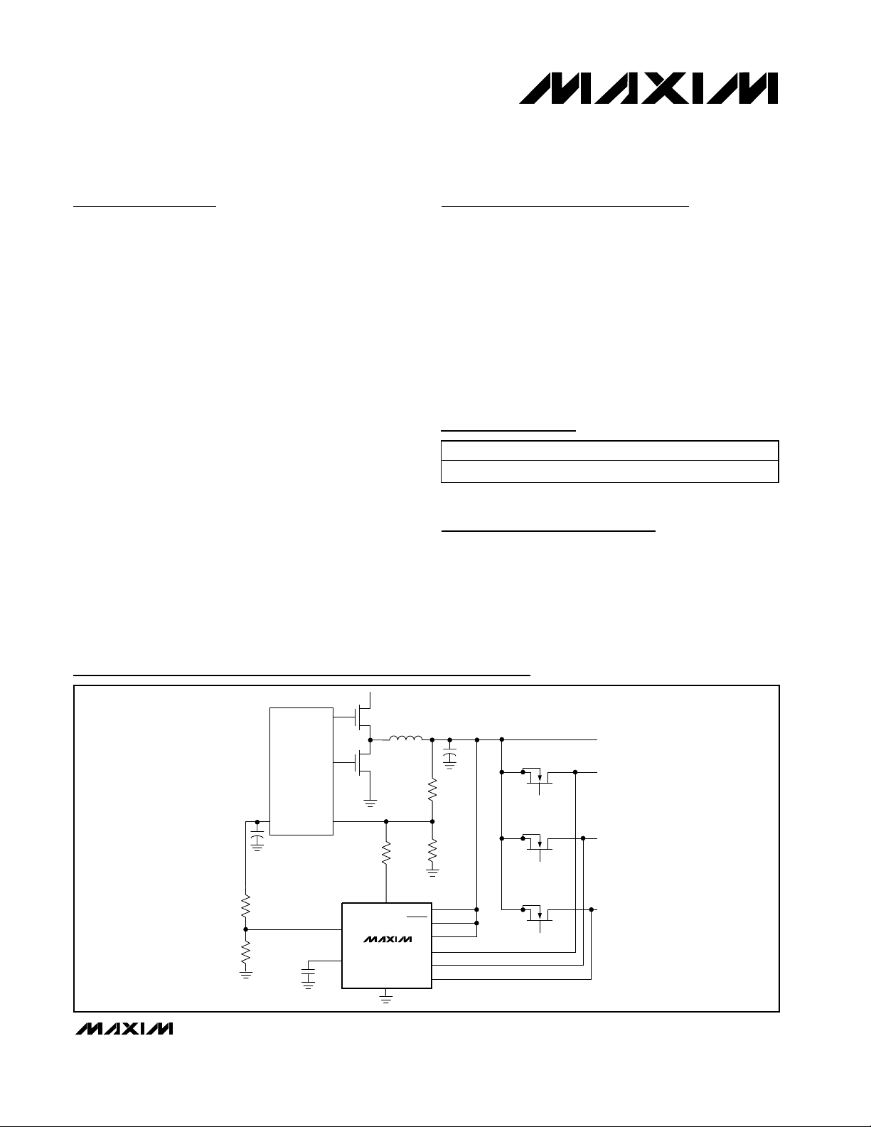
Typical Operating Circuit
PART TEMP. RANGE PIN-PACKAGE
MAX1804EUB -40°C to +85°C 10 µMAX
V
IN
DH
SYSTEM
SUPPLY
DL
R
TOP
FBREF
SHDN
IN1
IN2
IN3
IN4
R
BOTTOM
V+
R
OUT
OUT
ADJ
MAX1804
COMP
GND
V
A
OUT
V
B
OUT
V
C
OUT
D
V
OUT
Page 2
MAX1804
External Four-Input Feedback Integrator for
Power Supplies
2 _______________________________________________________________________________________
ABSOLUTE MAXIMUM RATINGS
ELECTRICAL CHARACTERISTICS
(TA= 0°C to +85°C, VV+ = 3.3V, V
ADJ
= 1.2V, V
OUT
= 2V, CV+ = 0.1µF, C
COMP
= 470pF. Typical values are at TA= +25°C, unless
otherwise noted.)
Stresses beyond those listed under “Absolute Maximum Ratings” may cause permanent damage to the device. These are stress ratings only, and functional
operation of the device at these or any other conditions beyond those indicated in the operational sections of the specifications is not implied. Exposure to
absolute maximum rating conditions for extended periods may affect device reliability.
V+, IN1, IN2, IN3, IN4, OUT, ADJ, SHDN to GND...…-0.3V, +6V
COMP to GND ....................................................-0.3V, V+ +0.3V
Continuous Power Dissipation (T
A
= +70°C)
10-Pin µMAX (derate 8.3mW/°C above +70°C) ..........667mW
Operating Temperature Extended Range ...........-40°C to +85°C
Junction Temperature ..................…………………………+150°C
Storage Temperature Range.……...……………-65°C to +165°C
Lead Temperature (soldering, 10s) .................................+300°C
PARAMETER CONDITIONS
U N IT S
Supply Voltage Range (V+) 2.7 5.5 V
Shutdown Supply Current (V+) SHDN = GND
1 µA
Quiescent Supply Current (V+) SHDN = V+ 25 35 µA
UVLO Threshold, Rising 2.5 2.6 V
UVLO Threshold, Falling 2.3 2.4 V
INTEGRATOR INPUTS IN1–IN4
IN_ Voltage Range 0 5.5 V
IN_ Offset VV+ = 2.7V to 5.5V -15 15
mV
V
ADJ
= 0.7V to 1.4V
V/V
V
IN_
= 4.75V to 4.85V, V
COMP
= 1.3V 12 30
48
µS
V
IN_
= 4.8V 1.5 2.7 µA
SHDN = GND 0.2 µA
VV+ = 0, V
SHDN
= 0 0.2 µA
IN_ Disable Threshold
V
ADJ
= 0.7V to 1.4V, V
ADJ
x 4, falling edge 87 90 93
%
V
ADJ
= 0.7V to 1.4V, rising edge 50
mV
ADJ INPUT
0.7 1.4 V
-20 20 nA
SHDN = GND 0.2 µA
VV+ = 0, V
SHDN
= 0 0.2 µA
COMP OUTPUT
V
COMP
= 1.3V, V
IN_
= 4.6V 1.6 2.0 2.4 µA
V
COMP
= 1.3V, V
IN_
= 5.0V 1.6 2.0 2.4 µA
Sink 1µA, V
IN_
= 5.0V 0.2 V
Source 1µA, V
IN_
= 4.6V 2.4 V
OUT OUTPUT
I
OUT
= 10 µA, V
IN_
= 4.6V 0.2 V
V
SHDN
= 0 0.1
VV+ = 0 0.1
V
IN_
= 5.0V 0.1
µA
V
COMP
= 1V to 2V 4 10 22 µS
IN_ Scale Factor
IN_ Transconductance
IN_ Bias Current
IN_ Shutdown Current
IN_ Leakage Current
IN_ Disable Threshold Hysteresis
ADJ Voltage Range
ADJ Bias Current
ADJ Shutdown Current
ADJ Leakage Current
COMP Source Current
COMP Sink Current
COMP Output Voltage Low
COMP Output Voltage High
OUT Output Voltage Low
OUT Output Leakage Current
OUT Transconductance
MIN TYP MAX
0.01
3.988 4.000 4.016
Page 3
MAX1804
External Four-Input Feedback Integrator for
Power Supplies
_______________________________________________________________________________________ 3
ELECTRICAL CHARACTERISTICS (continued)
(TA= 0°C to +85°C, VV+ = 3.3V, V
ADJ
= 1.2V, V
OUT
= 2V, CV+ = 0.1µF, C
COMP
= 470pF. Typical values are at TA= 25°C, unless oth-
erwise noted.)
PARAMETER CONDITIONS
MIN
TYP
MAX
U N IT S
SHDN INPUT
Logic Input Voltage High VV+ = 2.7V to 5.5V 2.0 V
Logic Input Voltage Low VV+ = 2.7V to 5.5V 0.6 V
Logic Input Current -1 1 µA
ELECTRICAL CHARACTERISTICS
(TA= -40°C to +85°C, VV+ = 3.3V, V
ADJ
= 1.2V, V
OUT
= 2V, CV+ = 0.1µF, C
COMP
= 470pF.) (Note 1)
PARAMETER CONDITIONS
U N IT S
Supply Voltage Range (V+) 2.7 5.5 V
Shutdown Supply Current (V+) SHDN = GND 1 µA
Quiescent Supply Current (V+) SHDN = V+ 35 µA
UVLO Threshold, Rising 2.6 V
UVLO Threshold, Falling 2.3 V
INTEGRATOR INPUTS IN1–IN4
IN_ Voltage Range 0 5.5 V
IN_ Offset VV+ = 2.7V to 5.5V -20 20
mV
V
ADJ
= 0.7V to 1.4V
V/V
V
IN_
= 4.75V to 4.85V, V
COMP
= 1.3V 12
60
µS
V
IN_
= 4.8V 2.7 µA
SHDN = GND 0.2 µA
VV+ = 0, V
SHDN
= 0 0.2 µA
IN_ Disable Threshold
V
ADJ
= 0.7V to 1.4V, V
ADJ
x 4, falling edge 87 93
%
ADJ INPUT
0.7 1.4 V
-30 30 nA
SHDN = GND 0.2 µA
V V+ = 0, V
SHDN
= 0 0.2 µA
COMP OUTPUT
V
COMP
= 1.3V, V
IN_
= 4.6V 1.6 2.4 µA
V
COMP
= 1.3V, V
IN_
= 5.0V 1.6 2.4 µA
Sink 1µA, V
IN_
= 5.0V 0.2 V
Source 1µA, V
IN_
= 0.6V 2.4 V
I
OUT
= 10µA, V
IN_
= 4.6V 0.2 V
V
SHDN
= 0 0.1
VV+ = 0 0.1
VIN = 5.0V 0.1
µA
OUT Transconductance V
COMP
= 1V to 2V 3 23 µS
IN_ Scale Factor
IN_ Transconductance
IN_ Bias Current
IN_ Shutdown Current
IN_ Leakage Current
ADJ Voltage Range
ADJ Bias Current
ADJ Shutdown Current
ADJ Leakage Current
COMP Source Current
COMP Sink Current
COMP Output Voltage Low
COMP Output Voltage High
OUT Output Voltage Low
OUT Output Leakage Current
MIN TYP MAX
3.98 4.02
Page 4
ELECTRICAL CHARACTERISTICS (continued)
(TA= -40°C to +85°C, VV+ = 3.3V, V
ADJ
= 1.2V, V
OUT
= 2V, CV+ = 0.1µF, C
COMP
= 470pF.) (Note 1)
MAX1804
External Four-Input Feedback Integrator for
Power Supplies
4 _______________________________________________________________________________________
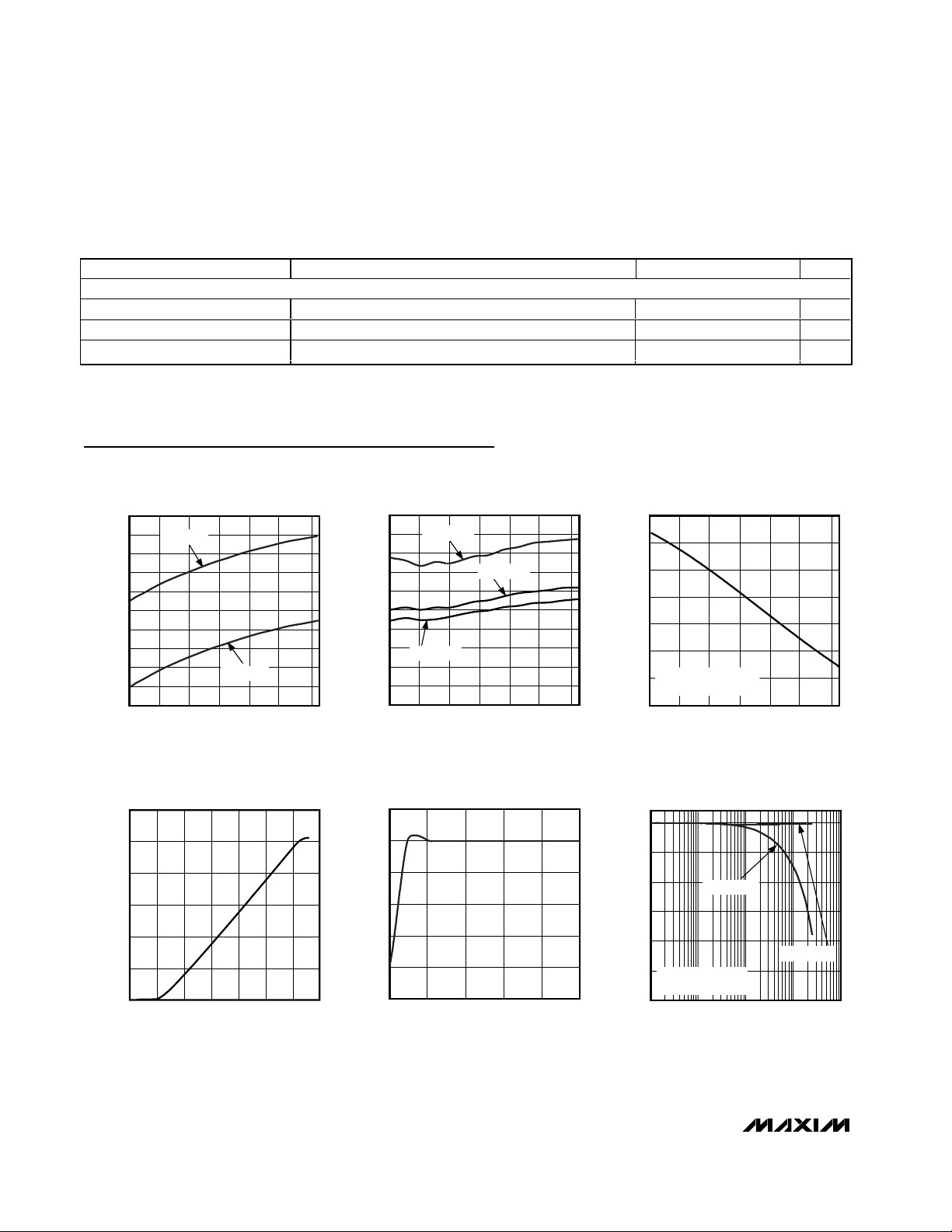
Typical Operating Characteristics
(VV+ = V
SHDN
= 3.3V, V
ADJ
= 1.2V, V
OUT
= 2V, C
COMP
= 470pF, TA= +25°C, unless otherwise noted.)
Note 1: Specifications to -40°C are guaranteed by design and not production tested.
PARAMETER CONDITIONS MIN TYP MAX U N IT S
SHDN INPUT
Logic Input Voltage High VV+ = 2.7V to 5.5V 2.0 V
Logic Input Voltage Low VV+ = 2.7V to 5.5V 0.6 V
Logic Input Current -1 1 µA
29.0
28.5
28.0
27.5
27.0
26.5
26.0
25.5
QUIESCENT CURRENT (µA)
25.0
24.5
24.0
-40 0-20 20 40 60 80
QUIESCENT CURRENT vs.
TEMPERATURE
VV+ = 5V
VV+ = 3.3V
TEMPERATURE (°C)
IN_REGULATION SET-POINT ERROR
vs. TEMPERATURE
0.050
V
0.045
MAX1804 toc01
0.040
0.035
0.030
0.025
0.020
0.015
0.010
IN_REGULATION SET-POINT ERROR (%)
0.005
0
-40
NOTE: Circuit of Figure 1.
= 0.7V
ADJ
V
= 1.4V
ADJ
V
= 1.2V
ADJ
0-20 20 40 60 80
TEMPERATURE (°C)
MAX1804 toc02
IN_ (TO COMP) TRANSCONDUCTANCE
34
32
30
28
26
24
IN_TRANSCONDUCTANCE (µS)
22
20
-40 0-20 20 40 60 80
vs. TEMPERATURE
V
∆
= 4.85V TO 4.75V
IN_
= 1.3V
V
COMP
TEMPERATURE (°C)
MAX1804 toc03
OUT CURRENT vs. COMP VOLTAGE
30
25
20
15
OUT CURRENT (µA)
10
5
0
0 1.5 2.00.5 1.0 2.5 3.0 3.5
COMP VOLTAGE (V)
MAX1804toc04
IN_SCALE FACTOR vs. ADJ VOLTAGE
4.05
4.00
3.95
3.90
IN_SCALE FACTOR
3.85
3.80
3.75
0.4
NOTE: Circuit of Figure 1.
ADJ VOLTAGE (V)
1.0 1.20.6 0.8 1.4
0
MAX1804toc05
-50
-100
-150
-200
CHANGE IN OUTPUT VOLTAGE (mV)
-250
-300
0.001
vs. OUTPUT CURRENT
MAX1804 OFF
V
= 5V (NOMINAL)
OUT
= 470pF
C
COMP
OUTPUT CURRENT (A)
NOTE: Application Circuit of Figure 2.
CHANGE IN OUTPUT VOLTAGE
MAX1804toc06
MAX1804 ON
1100.01 0.1
Page 5

MAX1804
External Four-Input Feedback Integrator for
Power Supplies
_______________________________________________________________________________________ 5
Typical Operating Characteristics (continued)
(VV+ = V
SHDN
= 3.3V, V
ADJ
= 1.2V, V
OUT
= 2V, C
COMP
= 470pF, TA= +25°C, unless otherwise noted.)
CH1
CH5
CH4
CH3
CH2
LOAD TRANSIENT RESPONSE
(APPLICATION CIRCUIT OF FIGURE2)
100µs/div
CH1 = I
; 1.00A/div
LOAD
; 500mV/div; AC-COUPLED (C
CH5 = V
IN1
; 500mV/div; AC-COUPLED (C
CH4 = V
IN1
; 500mV/div; AC-COUPLED (C
CH3 = V
IN1
; 500mV/div; AC-COUPLED (MAX1804 DISABLED)
CH2 = V
IN1
(MAX1653) = 8V
V
IN
STARTUP/SHUTDOWN WAVEFORM
COMP
COMP
COMP
= 1000pF)
= 470pF)
= 220pF)
MAX1804toc07
CH1
CH2
CHR4
CHR3
CHR2
CHR1
CH1 = I
CH2 = V
CHR4 = V
CHR3 = V
CHR2 = V
CHR1 = V
(MAX603) = 8V
V
IN
NOTE: Circuit of Figure 3.
AUTOMATIC INPUT DISABLE WAVEFORM
LOAD TRANSIENT RESPONSE
400µs/div
; 500mA/div
LOAD
; 500mV/div; AC-COUPLED (C
IN1
; 500mV/div; AC-COUPLED (C
IN1
; 500mV/div; AC-COUPLED (C
IN1
; 500mV/div; AC-COUPLED (C
IN1
; 500mV/div; AC-COUPLED (MAX1804 DISABLED)
IN1
MAX1804toc08
COMP
COMP
COMP
COMP
= 0.047µF)
= 1000pF)
= 2200pF)
= 4700pF)
0.5
0.01
CH1
CH2
CH1 = SHDN, 2V/div
; 200mV/div; DC OFFSET = 4.7V
CH2 = V
IN2
0.5A
I
LOAD =
(MAX1653) = 8V
V
IN
NOTE: Circuit of Figure 2.
200µs/div
MAX1804toc09
CHR1
CH1
CH2
CHR1 = V
CH1 = V
CH2 = V
V
NOTE: Circuit of Figure 2.
IN2 ENABLE
IN2 DISABLE IN2 DISABLE
200µs/div
; 5V/div
G(PFET)
; 200mV/div; DC OFFSET = 4.8V
IN1
; 2V/div
IN2
(MAX1653) = 8V
IN
MAX1804toc10
Page 6

MAX1804
External Four-Input Feedback Integrator for
Power Supplies
6 _______________________________________________________________________________________
Detailed Description
The MAX1804 is a precision external feedback integrator used for tight point-of-load regulation in power-management systems. The dynamic regulation of the output
is still controlled by the power-supply regulator. The
MAX1804 is used only to fine tune the output voltage,
removing load- and line-regulation errors and voltage
drops across switches and connectors that occur in the
power-supply distribution line.
The MAX1804 includes four remote-sense inputs and
an output that connects to a voltage regulator’s feedback divider. It can be used with any regulator or controller with a high-impedance feedback input. Its OUT
pin sinks current to increase the regulator’s set point so
that the four IN_ inputs are at or above MAX1804’s regulation set point, which is four times the voltage applied
to the ADJ pin. The MAX1804 monitors the input signals
and compares the lowest to the voltage set point. The
error between the input signal and the set point is integrated. The MAX1804 output stage generates a current
based on the integrator output to adjust the regulator’s
output voltage to meet the set point.
Pin Description
NAME PIN FUNCTION
IN1 1
Sense Input 1. Connect to one of up to four inputs to be monitored. If IN_ is the lowest active input,
IN_ will be regulated at 4 x V
ADJ
. If IN_ is less than 90% of the regulation set point (4 x V
ADJ
), it is
automatically disabled.
IN2 2 Sense Input 2
IN3 3 Sense Input 3
IN4 4 Sense Input 4
ADJ 5
Regulation Adjustment Input. The voltage at this input adjusts the regulation set point of
IN1–IN4.There is a 4x scale factor between V
ADJ
and the regulation set point.
GND 6 Ground
COMP 7
Integrator Capacitor Connection. Connect a capacitor (>100pF) to GND to set the integrator time
constant. See Integrator Gain-Bandwidth Product and Regulator Stability section.
OUT 8
O p en- D r ai n O utp ut. C an si nk at l east 10µ A i f any of the i np uts r em ai n b el ow the r eg ul ati on set p oi nt.
C onnect OU T to the feed b ack p oi nt of the r eg ul ator - d i vi d er r esi stor s. If OU T i s connected thr oug h a
r esi stor , i ts val ue r el ati ve to the r eg ul ator ’ s feed b ack- d i vi d er va l ues sets the m axi m um p osi ti ve
ad j ustm ent r ang e. S ee S etti ng the M axi m um Reg ul ator O utp ut Ad j ustm ent Incr ease secti on.
SHDN 9
Shutdown Control Input. When SHDN is low, the device is off and the supply current is reduced to
about 10nA. All inputs are in high-impedance state. When SHDN is high, the device is on.
V+ 10 Power-Supply Input. Bypass with 0.1µF capacitor to GND.
Figure 1. Test Circuit for MAX1804 IN_ Regulation Set Point
0.1µF
1M
1%
3.3V
3.3V
1k
1%
+10V
-10V
1k
1%
75k
1%
25k
1%
470pF
ADJ
COMP
EXTERNAL
REF
IN2
IN3
IN4
IN1
V+
OUT
MAX1804
MAX400
SHDN
Page 7

MAX1804
External Four-Input Feedback Integrator for
Power Supplies
_______________________________________________________________________________________ 7
The MAX1804 only sinks current at OUT (Figure 4). The
maximum sink current and maximum regulator voltage
increase are limited by the minimum guaranteed OUT
current of 10µA. The maximum regulator output voltage
increase can be further limited by including a resistor
between OUT and the feedback point of the regulator.
If any of the IN_ inputs fall to 90% of the regulation set
point, they are automatically disabled and OUT continues to regulate according to the lowest remaining
active input. See Automatic Input Disable.
Adjusting the Regulation Set Point
The MAX1804 monitors the voltage at the IN1–IN4
sense inputs and regulates the lowest active input to
four times the reference voltage at ADJ. The IN1–IN4
regulation set point is calculated as:
V
IN_
= 4 ✕V
ADJ
The total error in the MAX1804 regulation set point is:
total percentage error = [(IN_scale factor x V
ADJ
+
IN_offset) / (4 x V
ADJ
)] x 100%
The maximum IN_ voltage is 5.5V. Use the MAX1804 for
higher output voltages by using an external divider to
divide down the desired output voltage at the IN1–IN4
pins. Since the IN_ input bias current is fairly high (1.5µA
typ), choose the resistive divider accordingly.
Automatic Input Disable
The MAX1804 has an input buffer stage that monitors
the sense inputs (IN1–IN4) and connects the lowest to
its internal integrator (Figure 4). Each input is compared to 90% of the set point. If the input falls below
this value, the input buffer is disabled and the output
voltage is adjusted according to the lowest of the
remaining active inputs (see Automatic Input Disable in
Typical Operating Characteristics). If all four sense
4.5V TO 28V
VIN
VOUT
SHDN
SYNC
REF
3
10 16
1
2
3
14
11
15
13
12
8
9
7
DH
BST
VL
LX
DL
PGND
CSH
CSL
FB
6
6
4
3
1
5
827
2
5
3
4
1
V+
SHDN
N1B
IRF7303
D1
CMPSH-3
C4
0.1µF
N1A
IRF7303
D2
MBR0530
SKIP
SYNC
REF
GND
1M
SS
JU3
2
JU4
EXT
REF
COMP
ADJ
IN2
IN3
IN4
IN1
OUTV+
VL
C6
0.01µF
0.01µF
C5
0.33µF
100k
100k
JU2
JU1
3
VL
VL
2
3
1
C2
0.1µF
C1
22µF
35V
C7
220µF
10V
R
TOP
91k
1%
5V± 5%
PFET
I
LOAD
R
BOTTOM
100k
1%
562k
C3
4.7µF
16V
L1
15µH
R1
0.033Ω
1%
2
U1
MAX1653
MAX1804
SHDN
Figure 2. Application Circuit with Step-Down Regulator
Page 8

MAX1804
External Four-Input Feedback Integrator for
Power Supplies
8 _______________________________________________________________________________________
inputs are disabled, OUT is high impedance. Connect
any unused input to GND.
Setting the Maximum Regulator Output
Voltage Increase
The ratio between the maximum guaranteed OUT current of 10µA and the current in the regulator’s feedback
resistive divider determines the maximum increase. The
maximum increase in the regulator output voltage
depends on the regulator’s upper feedback resistor
(R
TOP
) and the sink current into OUT:
∆V
OUT
(MAX) = I
OUT
(MAX) x R
TOP
The maximum adjust current I
OUT
(MAX) can be further
limited with a resistor (R
OUT
) between OUT and the
feedback point of the regulator (see Typical Operating
Circuit):
I
OUT
(MAX) = VFB/ R
OUT
where VFBis the voltage at the regulator’s feedback
point.
Therefore:
∆V
OUT
(MAX) = VFBx R
TOP
/ R
OUT
and:
R
OUT
= VFBx R
TOP
/ ∆V
OUT
(MAX)
Place the regulator’s feedback resistors and R
OUT
close to the regulator’s feedback pin to reduce noise
pickup at the regulator’s feedback point, which can
cause unstable switching in the regulator (Figure 5).
Shutdown Mode
SHDN is a logic input that, when held low, places the
MAX1804 in its low-power shutdown mode, reducing
the supply current to 10nA (typ). The IN1–IN4, OUT,
and ADJ are high impedance when the MAX1804 is in
shutdown or when V+ is removed. Connect SHDN to
V+ for normal operation.
Undervoltage Lockout
The MAX1804 has an undervoltage lockout (UVLO) feature that deactivates the device when the supply voltage at V+ goes below 2.4V; IN1–IN4, OUT, and ADJ go
to high impedance and do not affect the regulator operation. Hysteresis holds the device in lockout until the
supply voltage at V+ rises above 2.6V.
Integrator Gain-Bandwidth Product
and Regulator Stability
The MAX1804 gain-bandwidth (GBW) product is set by
the external capacitor on COMP:
GBW = [4 x (IN_ transconductance)] / (2π✕C
COMP
)
The bandwidth is typically 40kHz with a 470pF capacitor on COMP.
For system stability, the integrator GBW product is typically set below the regulator circuit’s crossover frequency, if known. Switching regulators typically have
crossover frequencies well below their switching frequencies. Setting the MAX1804’s GBW product too high can
cause regulator loop instability, typically evidenced by
ringing after transients. Setting the GBW product unnecessarily low will slow the MAX1804’s loop response to
transients, although the regulator’s loop transient
response will remain unaffected (see Load Transient
Response in Typical Operating Characteristics).
Often the regulator’s crossover frequency varies with
load and is not easily found. If the regulator’s crossover
frequency is unknown, the MAX1804’s gain-bandwidth
product can be chosen empirically. Start with a fairly
low capacitor value (470pF is a good starting point)
and increase the value until the circuit is stable with all
loads. Then increase the value further to ensure design
margin. If transient response is unimportant, choose a
large COMP capacitor value (such as 2200pF), thereby
maximizing stability.
Figure 3. MAX1804 Used with Linear Regulator
COMP
ADJ
IN2
IN3
IN4
IN1
GND
V+ SET
10µF
2200pF
R
TOP
300k
R
TOP
600k
I
LOAD
0 TO
500mA
FDV 304P
5V TO
11V
1.25V
REFERENCE
MAX1804
SHDN
10µF
R
BOTTOM
100k
GND SET
OUT
IN
MAX603
OFF
Page 9

MAX1804
External Four-Input Feedback Integrator for
Power Supplies
_______________________________________________________________________________________ 9
Figure 4. MAX1804 Functional Block Diagram
V
BATT
V+
SYSTEM
DC/DC
FB3 FB5
GND
390k
UVLO
V+
EN
EN
SHDN
SHUTDOWN
LOGIC
OUT
EN
0.1µF
47k
51k
+5V SYSTEM SUPPLY
ONA
ONB
ONC
OND
MAX1804
IN1
3R
1R
SHDN
IN2
3R
1R
470pF
COMP
GND
g
m
EN
= 120µS
SHDN
EN
EN
9R1R
IN3
3R
1R
SHDN
IN4
3R
1R
SHDN
ADJ
Page 10

MAX1804
External Four-Input Feedback Integrator for
Power Supplies
10 ______________________________________________________________________________________
Applications Information
Layout Information
Proper layout is essential due to high current levels and
switching waveforms that generate noise. Place the
regulator’s feedback resistors and R
OUT
(from the regulator feedback point to OUT of MAX1804) close to the
regulator’s feedback point to prevent noise pickup
(Figure 5). Minimize leakage of the COMP capacitor and
traces around COMP because they cause IN_ set-point
errors according to the IN_ transconductance. A leakage
of I
COMP
at COMP will result in an error given by:
IN_ error voltage = I
COMP
/ (IN_ transconductance)
For a typical value of IN_ transconductance of 30µS, a
leakage of 0.1µA will result in an IN_ error voltage of
3mV in the set point.
Design Example (Step-Down
Converter Application)
Figure 2 is an example of an application circuit using
the MAX1804 for point-of-load regulation when using a
step-down controller (MAX1653). Use the following
design procedure to optimize the basic schematic.
Begin the design by establishing the following:
• Input voltage to the MAX1653 controller (7V to 20V)
• Typical output voltage and accuracy of MAX1653
(5V ±5%)
This gives a target of:
V
OUT
, min
= 5V - 5% = 4.75V
To minimize power dissipation, set regulator output
V
OUT, R
= 4.8V with MAX1653 feedback resistors.
Choose feedback resistors (R
TOP
and R
BOTTOM
) for
about 25µA current in the resistive divider for noise
immunity.
Therefore:
(R
TOP
+ R
BOTTOM
) = 4.8V / 25µA = 192kΩ
For the MAX1653, the voltage at its feedback point
V
FB
= 2.5V.
Choose R
TOP
= 91kΩ and therefore, R
BOTTOM
=
100kΩ.
If the desired adjustment range is +400mV, max OUT
current (MAX1804) is given by:
I
OUT
(MAX) = 0.4V / 91kΩ = 4.4µA
R
OUT
= VFB/ I
OUT
(MAX) = 2.5V / 4.4µA = 562kΩ
To guarantee that the output will not go below the target of 4.75V, including all error sources, set the
MAX1804 nominal regulation point to 4.85V.
Since:
IN_scale factor = 4 x V
ADJ
, V
ADJ
= 1.2125V
Divide the reference voltage down and bypass as
required if using the MAX1653 reference voltage as
shown in Figure 2. Assuming 0.1% resistor accuracy
and using the MAX1653 reference, the error budget
can be calculated as:
Reference Accuracy -1.6%
ADJ Divider Accuracy -0.2%
Scale Factor Error -0.4%
IN_ Offset Voltage (-15mV) -0.3%
Total -2.5%
This gives a worst-case output voltage of 4.73V, which is
below the target of 4.75V. The most-significant error
source is the MAX1653 reference. Therefore, use a better
reference, if available, in the system or increase the VADJ
to increase the worst-case output voltage to 4.75V.
The MAX1653 works well with the MAX1804’s GBW
product set at 40kHz, so use a 470pF capacitor on
COMP.
Chip Information
TRANSISTOR COUNT: 636
Figure 5. Proper Layout of Feedback Resistors for Regulator
R
BOTTOM
R
OUT
R
TOP
TO
MAX1804
FB
G
ND
MAX1653
SHORT COMPACT PLACEMENT
OF FEEDBACK RESISTORS
REDUCES NOISE PICKUP
Page 11

Maxim cannot assume responsibility for use of any circuitry other than circuitry entirely embodied in a Maxim product. No circuit patent licenses are
implied. Maxim reserves the right to change the circuitry and specifications without notice at any time.
11 ____________________Maxim Integrated Products, 120 San Gabriel Drive, Sunnyvale, CA 94086 408-737-7600
© 2000 Maxim Integrated Products Printed USA is a registered trademark of Maxim Integrated Products.
Package Information
Note: MAX1804 does not feature exposed pads
External Four-Input Feedback Integrator for
Power Supplies
MAX1804
 Loading...