

Page 1
General Description
The MAX1802 provides a complete power-supply solution for digital still cameras and video cameras by integrating two high-efficiency step-down DC-DC converters
and three auxiliary step-up controllers. This complete
solution is targeted for applications that use either three
to four alkaline cells or two lithium-ion (Li+) cells.
The main step-down DC-DC controller accepts inputs
from 2.5V to 11V and regulates a resistor-adjustable output from 2.7V to 5.5V. It uses a synchronous rectifier to
regulate the output with up to 94% efficiency. An
adjustable operating frequency (up to 1MHz) facilitates
designs for optimum size, cost, and efficiency.
The core step-down DC-DC converter accepts inputs
from 2.7V to 5.5V and regulates a resistor-adjustable
output from 1.25V to 5.5V. It delivers 500mA with up to
94% efficiency.
The three auxiliary step-up controllers can be used to
power the digital camera’s CCD, LCD, and backlight.
The MAX1802 also features expandability by supplying
power, an oscillator signal, and a reference to the
MAX1801, a low-cost slave DC-DC controller that supports step-up, single-ended primary inductance converter (SEPIC), and fly-back configurations.
The MAX1802 is available in a space-saving 32-pin
TQFP package (5mm x 5mm body), and the MAX1801
is available in an 8-pin SOT-23 package. An evaluation
kit (MAX1802EVKIT) featuring both devices is available
to expedite designs.
________________________Applications
Digital Still Cameras
Digital Video Cameras
Hand-Held Devices
Internet Access Tablets
PDAs
DVD Players
Features
♦ 2.5V to 11V Input Voltage Range
♦ Main DC-DC Controller
94% Efficiency
+2.7V to +5.5V Adjustable Output Voltage
Up to 100% Duty Cycle
Independent Shutdown
♦ Core DC-DC Converter
94% Efficiency
Up to 500mA Load Efficiency
Output Voltage Adjustable Down to 1.25V
Independent Shutdown
♦ Three Auxiliary DC-DC Controllers
Adjustable Maximum Duty Cycle
Independent Shutdown
♦ Power, Oscillator, and Reference Outputs to Drive
External Slave Controllers (MAX1801)
♦ Up to 1MHz Switching Frequency
♦ 3µA Supply Current in Shutdown Mode
♦ Internal Soft-Start
♦ Overload Protection for All DC-DC Converters
♦ Compact 32-Pin TQFP Package
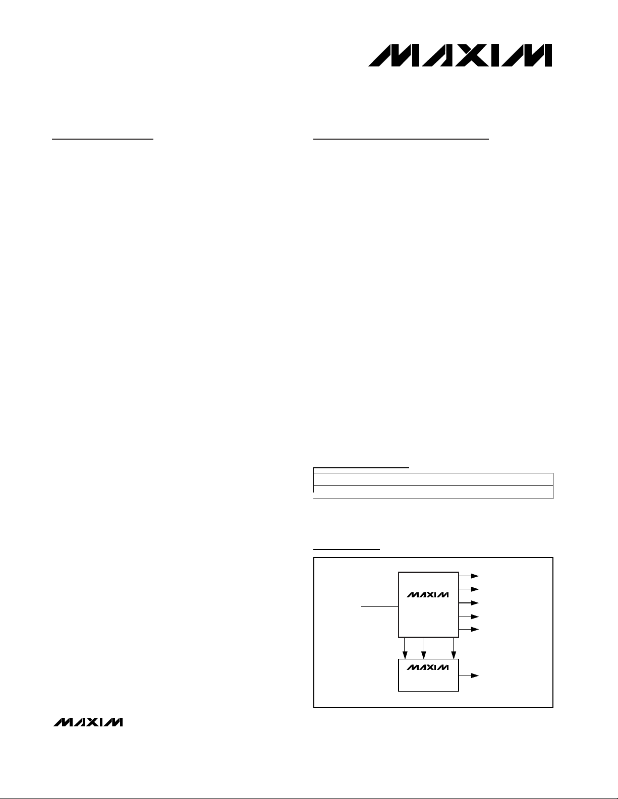
MAX1802
Digital Camera Step-Down
Power Supply
________________________________________________________________ Maxim Integrated Products 1
Typical Operating Circuit
19-1850; Rev 0; 10/00
For price, delivery, and to place orders, please contact Maxim Distribution at 1-888-629-4642,
or visit Maxim’s website at www.maxim-ic.com.
Ordering Information
Note: Refer to the separate data sheet for MAX1801EKA in an 8pin SOT.
Pin Configuration appears at end of data sheet.
32 TQFP
PIN-PACKAGETEMP. RANGE
-40°C to +85°CMAX1802EHJ
PART
MAIN
INPUT
2.5V TO 11V
OSC POWER REF
MAX1802
MASTER
CORE
CCD
CCFL
TFT
MAX1801
SLAVE
MOTOR
Page 2
MAX1802
Digital Camera Step-Down
Power Supply
2 _______________________________________________________________________________________
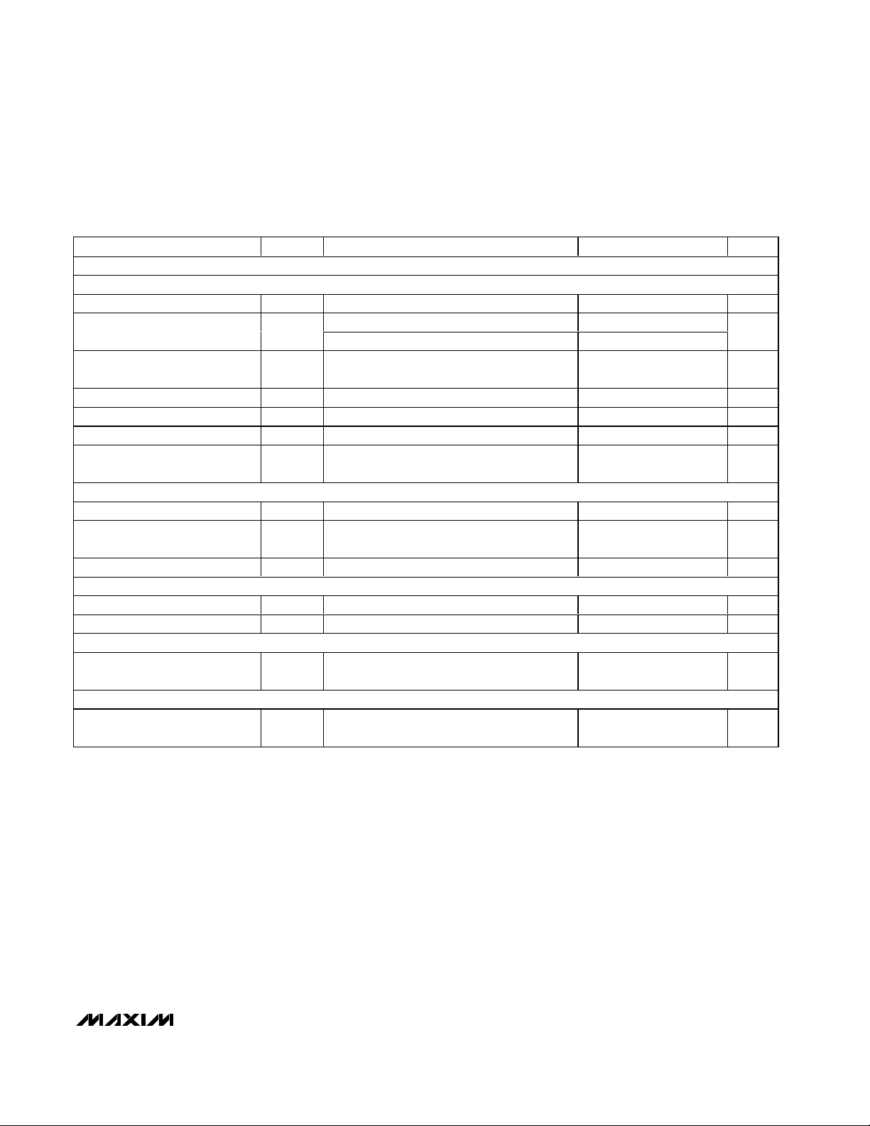
ABSOLUTE MAXIMUM RATINGS
ELECTRICAL CHARACTERISTICS
(Circuit of Figure 1, V
VDDM
= 6V, V
VDDC
= 3V, PGNDM = PGND = GND, DCON1 = REF, V
ONM
= 3V, V
ONC
= V
ON1
= V
DCON2
=
V
DCON3
= 0, TA= 0°C to +85°C, unless otherwise noted. Typical values are at TA= +25°C.)
Stresses beyond those listed under “Absolute Maximum Ratings” may cause permanent damage to the device. These are stress ratings only, and functional
operation of the device at these or any other conditions beyond those indicated in the operational sections of the specifications is not implied. Exposure to
absolute maximum rating conditions for extended periods may affect device reliability.
VDDM, VH, ONM to GND .......................................-0.3V to +12V
PGNDM, PGND to GND ........................................-0.3V to +0.3V
VH to VDDM .............................................................-6V to +0.3V
VL to VDDM ............................................................-12V to +0.3V
VL, ONC, ON1, FB_, DCON_ to GND ......................-0.3V to +6V
VDDC, REF, OSC, COMP_ to GND ..............-0.3V to (VL + 0.3V)
DHM, DLM to PGNDM............................-0.3V to (VDDM + 0.3V)
LXM to PGNDM ......................................-0.6V to (VDDM + 0.6V)
DL1, DL2, DL3, LXC to PGND ................-0.3V to (VDDC + 0.3V)
Continuous Power Dissipation (TA= +70°C)
32-Pin TQFP (derate 11.1mW/°C above +70°C)........889mW
Operating Temperature Range ...........................-40°C to +85°C
Junction Temperature......................................................+150°C
Storage Temperature Range. ............................-65°C to +150°C
Lead Temperature (soldering, 10s) .................................+300°C
PARAMETER SYMBOL CONDITIONS MIN TYP MAX UNITS
GENERAL
Input Voltage Range V
IN
2.5 11 V
SUPPLY CURRENT
Shutdown Supply Current
(from VDDM and VDDC)
Main DC-DC Converter
Supply Current (from VDDM)
Main DC-DC Converter
Supply Current (from VDDC)
Main plus Core Supply Current
(from VDDC)
Main plus Auxiliary 1
Supply Current (from VDDC)
Main plus Auxiliary 2
Supply Current (from VDDC)
Main plus Auxiliary 3
Supply Current (from VDDC)
Total Supply Current
(from VDDC)
V
V
V
V
V
V
= 0 3 20 µA
ONM
V
= 1.5V, V
FBM
V
= 1.5V, V
FBM
= 1.5V, V
FBM
= V
FBM
FBC
= V
FBM
FB1
= V
FBM
FB2
= V
FBM
FB3
V
= V
FBM
ONC
= V
FBC
ON1
V
VL REGULATOR
VL Output Voltage 6V < V
VL Supply Rejection 3.5V < V
VL Undervoltage Lockout
Threshold
VL Switchover Voltage to
VDDC
VL rising, 40mV hysteresis 2.25 2.40 2.50 V
VL rising, 100mV hysteresis 2.3 2.4 2.5 V
< 11V, 0.1mA < I
VDDM
VDDM
VL to VDDC Switch Resistance 7 Ω
= 0 370 600
VDDC
= 3V 35 55
VDDC
= 3V 270 450 µA
VDDC
= 1.5V, V
= 1.5V, V
= 1.5V, V
= 1.5V, V
= V
FB1
= V
DCON2
< 11V, V
= 3V 410 700 µA
ONC
= 3V 470 750 µA
ON1
= 3V 470 750 µA
DCON2
= 3V 470 750 µA
DCON3
= V
= V
FB2
= V
VDDC
= 1.5V,
FB3
= 3V
DCON3
< 10mA 2.83 3.00 3.12 V
LOAD
= 0 3 %
960 1700 µA
µA
Page 3
MAX1802
Digital Camera Step-Down
Power Supply
_______________________________________________________________________________________ 3
ELECTRICAL CHARACTERISTICS (continued)
(Circuit of Figure 1, V
VDDM
= 6V, V
VDDC
= 3V, PGNDM = PGND = GND, DCON1 = REF, V
ONM
= 3V, V
ONC
= V
ON1
= V
DCON2
=
V
DCON3
= 0, TA= 0°C to +85°C, unless otherwise noted. Typical values are at TA= +25°C.)
)
Idle Mode is a trademark of Maxim Integrated Products.
PARAMETER SYMBOL CONDITIONS MIN TYP MAX UNITS
REFERENCE
Reference Output Voltage V
REF Load Regulation 10µA <
REF Line Rejection 2.7V < V
REF Undervoltage Lockout
Threshold
OSCILLATOR
OSC Discharge Trip Level OSC rising 1.225 1.250 1.275 V
OSC Input Bias Current V
OSC Discharge Resistance V
OSC Discharge Pulse Width 100 ns
LOGIC INPUTS (ONM, ONC, ON1)
Input Low Level V
Input High Level V
Input Leakage Current
MAIN DC-DC CONVERTER
Main Output Voltage Adjust
Range
Main Idle Mode™ Threshold
Main Current-Sense Amplifier
Voltage Gain
Main N Channel Turn-Off
Threshold
Main Slope Compensation
Gain
MAIN ERROR AMPLIFIER
FBM Regulation Voltage Unity gain configuration, FBM = COMPM 1.233 1.248 1.263 V
FBM to COMPM
Transconductance
FBM Input Leakage Current V
COMPM Minimum Output
Voltage
COMPM Maximum Output
Voltage
I
REF
= 20µA 1.235 1.248 1.260 V
REF
< 200µA 5 9 mV
I
REF
< 5.5V 1 5 mV
OUT
REF rising, 20mV hysteresis 0.9 1 1.1 V
= 1.1V 0.2 100 nA
OSC
= 1.5V 30 100 Ω
OSC
0.4 V
ONM 1.8
ONC, ON1 1.6
ONM: V
ONC, ON1: V
= 0 or 11V;
IN
IN
= 0 or 5V
0.01 1 µA
2.7 5.5 V
V
= 0.625V, measured between VDDM
OSC
and LXM
8 20 32 mV
Measured between VDDM and LXM 8.4 9.3 10.2 V/V
V
A
VCSM
IL
IH
OUT
Measured between LXM and PGNDM -26 -17 -8 mV
A
VSWM
G
EA
V
V
COMPM (MAX
0.16 0.20 0.24 V/V
Unity gain configuration, FBM = COMPM,
-5µA < I
FBM
FBM
V
FBM
< 5µA
LOAD
= 1.35V 5 100 nA
= 1.35V, COMPM open 0.3 V
= 1.15V, COMPM open 2.00 2.14 2.27 V
70 100 160 µS
V
Page 4
MAX1802
Digital Camera Step-Down
Power Supply
4 _______________________________________________________________________________________
)
ELECTRICAL CHARACTERISTICS (continued)
(Circuit of Figure 1, V
VDDM
= 6V, V
VDDC
= 3V, PGNDM = PGND = GND, DCON1 = REF, V
ONM
= 3V, V
ONC
= V
ON1
= V
DCON2
=
V
DCON3
= 0, TA= 0°C to +85°C, unless otherwise noted. Typical values are at TA= +25°C.)
PARAMETER SYMBOL CONDITIONS MIN TYP MAX UNITS
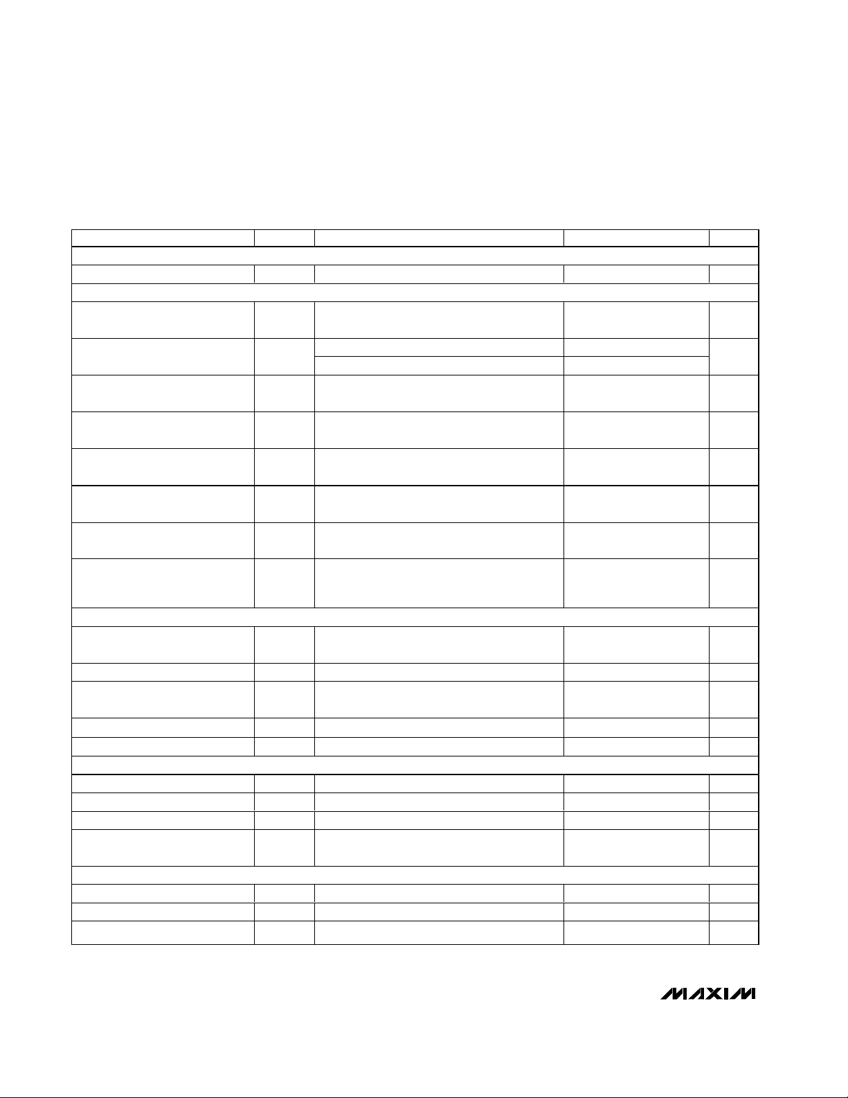
MAIN SOFT-START
Soft-Start Interval OSC falling edge 1024
MAIN DRIVERS (DHM, DLM)
Output Low Voltage I
Output High Voltage I
= 10mA 0.11 V
SINK
= 10mA
SOURCE
V
VDDM
0.11
-
OSC
cycles
V
Driver Resistance I
Drive Current
CORE DC-DC CONVERTER (V
Core Output Voltage Adjust
Range
= 3V)
ONC
V
OUT
Core Idle Mode Threshold V
Core Current-Sense Amplifier
Transresistance
Core Slope Compensation Gain A
CORE ERROR AMPLIFIER (V
ONC
R
CSC
VSWC
= 3V)
= 10mA, I
DHM
Sourcing or sinking,
or VVL = V
V
DHM
= 10mA 4 11 Ω
DLM
VDDM
/ 2
400 mA
1.25 5.5 V
= 0.625V 70 190 320 mA
OSC
0.7 1.0 1.3 V/A
0.16 0.20 0.24 V/V
FBC Regulation Voltage Unity gain configuration, FBC = COMPC 1.233 1.248 1.263 V
FBC to COMPC
Transconductance
FBC Input Leakage Current V
COMPC Minimum Output
Voltage
COMPC Maximum Output
Voltage
CORE SOFT-START (V
Soft-Start Interval 1024
CORE POWER SWITCHES (V
LXC Leakage Current V
Switch On-Resistance
P-Channel Current Limit V
N-Channel Turn-Off Current 18 100 180 mA
ONC
= 3V)
ONC
G
EA
V
COMPM (MAX
= 3V)
R
DSN
R
DSP
Unity gain configuration, FBC = COMPC,
-5µA < I
FBC
V
FBC
V
FBC
LXC
N-channel, I
P-channel, I
OSC
< 5µA
LOAD
= 1.35V 5 100 nA
= 1.35V, COMPC open 0.3 V
= 1.15V, COMPC open 2.00 2.14 2.27 V
= 0, 5.5V 0.01 20 µA
= 0.75A 150 350
LXC
= 0.75A 180 400
LXC
= 0.625V 0.75 A
70 100 160 µS
OSC
cycles
mΩ
Page 5
MAX1802
Digital Camera Step-Down
Power Supply
_______________________________________________________________________________________ 5
ELECTRICAL CHARACTERISTICS (continued)
(Circuit of Figure 1, V
VDDM
= 6V, V
VDDC
= 3V, PGNDM = PGND = GND, DCON1 = REF, V
ONM
= 3V, V
ONC
= V
ON1
= V
DCON2
=
V
DCON3
= 0, TA= 0°C to +85°C, unless otherwise noted. Typical values are at TA= +25°C.)
PARAMETER SYMBOL CONDITIONS MIN TYP MAX UNITS
AUXILIARY DC-DC CONTROLLERS 1, 2, 3 (V
ON1
= V
_ = 3V)
CON
INTERNAL CLOCK
OSC Clock Low Trip Level OSC falling edge 0.2 0.25 0.3 V
V
_ = 0.625V 0.575 0.625 0.675
DCON
OSC Clock High Trip Level
Maximum Duty Cycle
Adjustment Range
Maximum Duty Cycle V
Default Maximum Duty Cycle V
DCON_ Input Leakage Current V
DCON_ Input Sleep-Mode
Threshold
V
V
_ = 1.25V to V
DCON
_ = 0.625V 43 %
DCON
_ = 1.25V to V
DCON
_ = 0V to 3V 0.01 1 µA
DCON
_ rising, 50mV hysteresis 0.35 0.4 0.45 V
DCON
VL
VL
1.00 1.05 1.10
40 90
76 %
V
%
AUXILIARY ERROR AMPLIFIER
FB_ Regulation Voltage Unity gain configuration, FB_ = COMP_ 1.233 1.248 1.263 V
FB_ to COMP_
Transconductance
G
FB_ Input Leakage Current V
Unity gain configuration, FB_ = COMP_,
EA
-5µA < ILOAD < 5µA
_ = 1.35V 5 100 nA
FB
70 100 160 µs
AUXILIARY DRIVERS (DL1, DL2, DL3)
DL_ Driver Resistance Output high or low 4 11 Ω
DL_ Drive Current Sourcing or sinking, V
DL
_ = V
/ 2 400 mA
VDDC
AUXILIARY SOFT-START
Soft-Start Interval 1024
AUXILIARY SHORT-CIRCUIT PROTECTION
Fault Interval 1024
OSC
cycles
OSC
cycles
Page 6
MAX1802
Digital Camera Step-Down
Power Supply
6 _______________________________________________________________________________________
ELECTRICAL CHARACTERISTICS
(Circuit of Figure 1, V
VDDM
= 6V, V
VDDC
= 3V, PGNDM = PGND = GND, DCON1 = REF, V
ONM
= 3V, V
ONC
= V
ON1
= V
DCON2
=
V
DCON3
= 0, TA = -40°C to +85°C, unless otherwise noted.) (Note 1)
PARAMETER
GENERAL
Input Voltage Range V
SUPPLY CURRENT
Shutdown Supply Current
(from VDDM and VDDC)
Main DC-DC Converter
Supply Current (from VDDM)
Main DC-DC Converter
Supply Current (from VDDC)
Main plus Core Supply Current
(from VDDC)
Main plus Auxiliary 1 Supply
Current (from VDDC)
Main plus Auxiliary 2 Supply
Current (from VDDC)
Main plus Auxiliary 3 Supply
Current (from VDDC)
Total Supply Current
(from VDDC)
VL REGULATOR
VL Output Voltage
VL Supply Rejection 3.5V < V
VL Undervoltage Lockout
Threshold
VL Switchover Voltage to VDDC V
VL to VDDC Switch Resistance 7 Ω
REFERENCE
Reference Output Voltage V
REF Load Regulation 10µA < I
REF Line Rejection 2.7V < V
REF Undervoltage Lockout
Threshold
OSCILLATOR
OSC Discharge Trip Level OSC rising 1.225 1.275 V
OSC Input Bias Current V
OSC Discharge Resistance V
SYMBOL
IN
V
V
V
V
V
V
V
REF
2.5 11 V
= 0 20 µA
ONM
V
= 1.5V, V
FBM
V
= 1.5V, V
FBM
= 1.5V, V
FBM
= V
FBM
= V
FBM
= V
FBM
= V
FBM
V
= V
FBM
= V
V
ONC
V
DCON3
6V < V
VDDM
0.1mA < I
rising, 40mV hysteresis 2.25 2.50 V
L
rising, 100mV hysteresis 2.3 2.5 V
L
I
= 20µA 1.230 1.262 V
REF
CONDITIONS
= 0 600
VDDC
= 3V 55
VDDC
= 3V 450 µA
VDDC
= 1.5V, V
FBC
= 1.5V, V
FB1
= 1.5V, V
FB2
= 1.5V, V
FB3
= V
FBC
FB1
= V
ON1
= 3V
LOAD
VDDM
REF
OUT
DCON1
< 11V,
< 10mA
< 11V, V
< 200µA 9 mV
< 5.5V 5 mV
= 3V 700 µA
ONC
= V
ON1
DCON1
= 3V 750 µA
DCON2
= 3V 750 µA
DCON3
= V
= V
FB2
= V
DCON2
= 0 3 %
VDDC
= 3V 750 µA
= 1.5V,
FB3
=
MIN
TYP MAX UNITS
1700 µA
2.83 3.12 V
REF rising, 20mV hysteresis 0.9 1.1 V
= 1.1V 100 nA
OSC
= 1.5V 100 Ω
OSC
µA
Page 7

MAX1802
Digital Camera Step-Down
Power Supply
_______________________________________________________________________________________ 7
ELECTRICAL CHARACTERISTICS (continued)
(Circuit of Figure 1, V
VDDM
= 6V, V
VDDC
= 3V, PGNDM = PGND = GND, DCON1 = REF, V
ONM
= 3V, V
ONC
= V
ON1
= V
DCON2
=
V
DCON3
= 0, TA = -40°C to +85°C, unless otherwise noted.) (Note 1)
)
PARAMETER
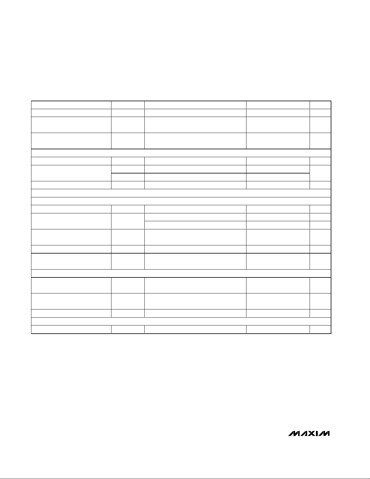
LOGIC INPUTS (ONM, ONC, ON1)
Input Low Level V
Input High Level V
Input Leakage Current
MAIN DC-DC CONVERTER
Main Output Voltage Adjust Range V
Main Idle Mode Threshold
Main Current-Sense Amplifier
Voltage Gain
Main Zero-Crossing Threshold Measured between LXM and PGNDM -20 -8 mV
Main Slope Compensation Gain A
MAIN ERROR AMPLIFIER
FBM Regulation Voltage Unity gain configuration, FBM = COMPM 1.230 1.265 V
FBM to COMPM
Transconductance
FBM Input Leakage Current V
COMPM Minimum Output
Voltage
COMPM Maximum Output
Voltage
MAIN DRIVERS (DHM, DLM)
Output Low Voltage I
Output High Voltage I
Driver Resistance I
CORE DC-DC CONVERTER (V
Core Output Voltage Adjust
Range
Core Idle Mode Threshold V
Core Current-Sense Amplifier
Transresistance
Core Slope Compensation Gain A
CORE ERROR AMPLIFIER (V
FBC Regulation Voltage Unity gain configuration, FBC = COMPC 1.230 1.265 V
FBC to COMPC
Transconductance
SYMBOL
IL
IH
0.4 V
ONM 1.8
ONC, ON1 1.6
ONM: V
ONC, ON1: V
CONDITIONS
= 0 or 11V;
IN
IN
= 0 or 5V
MIN TYP MAX UNITS
1 µA
V
OUT
A
VCSM
VSWM
G
EA
V
V
COMPM(MAX
= 3V)
ONC
V
OUT
R
CSC
VSWC
= 3V)
ONC
G
EA
2.7 5.5 V
V
= 0.625V, measured between
OSC
VDDM and LXM
2 35 mV
Measured between VDDM and LXM 8.4 10.2 V/V
0.16 0.24 V/V
U ni ty g ai n confi g ur ati on, FBM = C OM P M ,
- 5µA < I
FBM
FBM
V
FBM
SINK
SOURCE
DHM
< 5µA
LOA D
= 1.35V 100 nA
= 1.35V, COMPM open 0.3 V
= 1.15V, COMPM open 2.00 2.27 V
= 10mA 0.11 V
= 10mA
= 10mA, I
= 10mA 11 Ω
DLM
70 160 µS
V
-
VDDM
0.11
V
1.25 5.5 V
= 0.625V 40 360 mA
OSC
0.7 1.3 V/A
0.16 0.24 V/V
U ni ty g ai n confi g ur ati on, FBC = C OM P C ,
- 5µA < I
LOA D
< 5µA
70 160 µS
Page 8
MAX1802
Digital Camera Step-Down
Power Supply
8 _______________________________________________________________________________________
)
ELECTRICAL CHARACTERISTICS (continued)
(Circuit of Figure 1, V
VDDM
= 6V, V
VDDC
= 3V, PGNDM = PGND = GND, DCON1 = REF, V
ONM
= 3V, V
ONC
= V
ON1
= V
DCON2
=
V
DCON3
= 0, TA = -40°C to +85°C, unless otherwise noted.) (Note 1)
Note 1: Specifications to -40°C are guaranteed by design and not production tested.
PARAMETER SYMBOL CONDITIONS MIN TYP MAX UNITS
FBC Input Leakage Current V
COMPC Minimum Output
Voltage
COMPC Maximum Output
Voltage
CORE POWER SWITCHES (V
LXC Leakage Current V
Switch On-Resistance
N-Channel Turn-Off Current 5 190 mA
AUXILIARY DC-DC CONTROLLERS 1, 2, 3 (V
INTERNAL CLOCK
OSC Clock Low Trip Level OSC falling edge 0.2 0.3 V
OSC Clock High Trip Level
Maximum Duty Cycle
Adjustment Range
DCON_ Input Leakage Current V
DCON_ Input Sleep-Mode
Threshold
AUXILIARY ERROR AMPLIFIER
ONC
= 1.35V 100 nA
FBC
V
V
COMPC(MAX
= 3V)
R
DSN
R
DSP
ON1
V
= 1.35V, COMPC open 0.3 V
FBC
V
= 1.15V, COMPC open 2.00 2.27 V
FBC
= 0, 5.5V 20 µA
LXC
N-channel, I
P-channel, I
= V
DCON
V
_ = 0.625V 0.575 0.675 V
DCON
V
_ = 1.25V to V
DCON
_ = 0V to 3V 1 µA
DCON
_ rising, 50mV hysteresis 0.35 0.45 V
DCON
= 0.75A 350
LXC
= 0.75A 400
LXC
_= 3V)
VL
1.00 1.10
40 90
mΩ
%
FB_ Regulation Voltage Unity gain configuration, FB_ = COMP_ 1.230 1.265 V
FB_ to COMP_
Transconductance
G
EA
FB_ Input Leakage Current V
Unity gain configuration, FB_ = COMP_,
LOAD
< 5µA
-5µA < I
_ = 1.35V 100 nA
FB
70 160 µs
AUXILIARY DRIVERS (DL1, DL2, DL3)
DL_ Driver Resistance Output high or low 11 Ω
Page 9

MAX1802
Digital Camera Step-Down
Power Supply
_______________________________________________________________________________________ 9
Typical Operating Characteristics
(Circuit of Figure 1, V
VDDM
= 6V, V
VDDC
= 3.3V, V
ONM
= 3V, V
ONC
= V
ON1
= V
DCON2
= V
DCON3
= 0, TA = +25°C, unless otherwise
noted.)
100
0
1 10 100 1000 10,000
EFFICIENCY vs. LOAD CURRENT
(MAIN CONVERTER)
20
MAX1802 toc01
LOAD CURRENT (mA)
EFFICIENCY (%)
40
60
80
70
50
30
10
90
V
OUT
= 3.3V
VIN = +5V
VIN = +7.2V
VIN = +11V
100
0
1 10 100 1000 10,000
EFFICIENCY vs. LOAD CURRENT
(MAIN CONVERTER)
20
MAX1802 toc02
LOAD CURRENT (mA)
EFFICIENCY (%)
40
60
80
70
50
30
10
90
V
OUT
= +5V
VIN = +7.2V
VIN = +11V
100
0
1 10 100 1000
EFFICIENCY vs. LOAD CURRENT
(CORE CONVERTER)
20
MAX1802 toc04
LOAD CURRENT (mA)
EFFICIENCY (%)
40
60
80
70
50
30
10
90
VIN = +5V
VIN = +3.3V
V
OUT
= +2.5V
0
20
60
40
80
100
0.4 0.6 0.70.5 0.8 0.9 1.0 1.1 1.2
MAXIMUM DUTY CYCLE vs. V
DCON
_
MAX1802 toc05
V
DCON
_ (V)
MAXIMUM DUTY CYCLE (%)
0
20
60
40
80
100
0 400200 600 800 1000
DEFAULT MAXIMUM DUTY CYCLE
vs. FREQUENCY
MAX1802 toc06
FREQUENCY (kHz)
DEFAULT MAXIMUM DUTY CYCLE (%)
C
OSC
= 470pF
1000
0
1 10 100 1000
OSCILLATOR FREQUENCY
vs. R
OSC
200
MAX1802 toc07
R
OSC
(kΩ)
OSCILLATOR FREQUENCY (kHz)
400
600
800
C
OSC
= 470pF
C
OSC
= 220pF
C
OSC
= 100pF
C
OSC
= 47pF
0
2
6
4
8
10
042681012
MAX1802 toc08
INPUT VOLTAGE (V)
SHUTDOWN CURRENT (µA)
SHUTDOWN CURRENT
vs. INPUT VOLTAGE
EFFICIENCY vs. LOAD CURRENT
(CORE CONVERTER)
100
90
80
70
60
50
40
EFFICIENCY (%)
30
20
10
0
1 10 100 1000
VIN = +5V
VIN = +2.5V
VIN = +3.3V
LOAD CURRENT (mA)
MAX1802 toc03
V
= +1.8V
OUT
Page 10

1.247
1.249
1.248
1.251
1.250
1.252
1.253
0 10050 150 200 250
MAX1802 toc10
REFERENCE CURRENT (µA)
REFERENCE VOLTAGE (V)
REFERENCE VOLTAGE
vs. REFERENCE CURRENT
0
20
10
40
30
50
60
110010 1000 10,000
MAX1802 toc11
FREQUENCY (kHz)
SMALL-SIGNAL RESPONSE (dB)
FB_ TO COMP_ SMALL-SIGNAL
OPEN-LOOP FREQUENCY RESPONSE
MAX1802
Digital Camera Step-Down
Power Supply
10 ______________________________________________________________________________________
Typical Operating Characteristics (continued)
(Circuit of Figure 1, V
VDDM
= 6V, V
VDDC
= 3.3V, V
ONM
= 3V, V
ONC
= V
ON1
= V
DCON2
= V
DCON3
= 0, TA = +25°C, unless otherwise
noted.)
1ms/div
MAIN OUTPUT STARTUP RESPONSE
MAX1802 toc12
0V
0V
0A
V
ONM
5V/div
V
MAIN
2V/div
I
OUT
200mA/div
1ms/div
CORE OUTPUT STARTUP RESPONSE
MAX1802 toc13
0V
0V
0A
V
ONC
5V/div
V
CORE
2V/div
I
OUT
100mA/div
1ms/div
AUXILIARY CONTROLLER
STARTUP RESPONSE
MAX1802 toc14
VON_
5V/div
V
OUT
2V/div
I
OUT
200mA/div
0V
0V
0A
1.240
1.245
1.250
1.255
1.260
MAX1802 toc09
TEMPERATURE (°C)
REFERENCE VOLTAGE (V)
-40 20 40-20 0 60 80
REFERENCE VOLTAGE
vs. TEMPERATURE
Page 11

MAX1802
Digital Camera Step-Down
Power Supply
______________________________________________________________________________________ 11
Typical Operating Characteristics (continued)
(Circuit of Figure 1, V
VDDM
= 6V, V
VDDC
= 3.3V, V
ONM
= 3V, V
ONC
= V
ON1
= V
DCON2
= V
DCON3
= 0, TA = +25°C, unless otherwise
noted.)
1ms/div
STARTUP SEQUENCE
MAX1802 toc15
0V
0V
0A
V
ONM
5V/div
V
MAIN
2V/div
V
CORE
2V/div
400µs/div
MAIN OUTPUT
LOAD-TRANSIENT RESPONSE
MAX1802 toc16
V
OUT
AC-COUPLED
100mV/div
I
LOAD
200mA/div
0A
C
OUT
= 100µF
500µs/div
CORE OUTPUT
LOAD-TRANSIENT RESPONSE
MAX1802 toc17
V
OUT
AC-COUPLED
200mV/div
I
LOAD
100mA/div
0A
V
OUT
= 2.5V
400µs/div
AUXILIARY OUTPUT
LOAD-TRANSIENT RESPONSE
MAX1802 toc18
V
OUT
AC-COUPLED
100mV/div
I
LOAD
200mA/div
0A
2.5ms/div
MAIN TRANSIENT RESPONSE
SUBJECT TO CORE TRANSIENT
MAX1802 toc19
V
OUT
(MAIN)
AC-COUPLED
20mV/div
I
LOAD
(CORE)
100mA/div
0A
V
OUT
= 2.5V
Page 12

MAX1802
Digital Camera Step-Down
Power Supply
12 ______________________________________________________________________________________
Pin Description
PIN NAME FUNCTION
1 FBM
2 COMPM
3 ONM
4 VH
5 VDDM
6 DHM
7
8 DLM
9 PGNDM
10 OSC
LXM
Main DC-DC Converter Feedback Input. Connect a feedback resistive voltage-divider from the output
to FBM to set the main output voltage. Regulation voltage is V
Compensation for Main Controller. Output of main transconductance error amplifier. Connect a series
resistor and capacitor to GND to compensate the main control loop (see Compensation Design).
Main Converter Enable Input. High level turns on the main converter and VL regulator. Connect ONM
to VDDM to automatically start the converter. When the main converter is off, all other outputs are
disabled.
Internal Bias Voltage. VH provides bias to the main controller. Bypass VH to VDDM with a 0.1µF or
greater ceramic capacitor.
Battery Input. VDDM supplies power to the IC and also serves as a high-side current-sense input
for the main DC-DC controller. Connect VDDM as close as possible to the source of the external
P-channel switching MOSFET for the main controller.
External P-Channel MOSFET Gate-Drive Output for Main Controller. DHM swings between VDDM and
PGNDM with 400mA (typ) drive current. Connect DHM to the gate of the external P-channel switching
MOSFET for the main controller.
Main DC-DC Controller Current-Sense Input. Connect LXM to the drains of the external P- and Nchannel switching MOSFETs for the main converter. LXM serves as the current-sense input for both
P- and N-channel switching MOSFETs. Connect LXM as close as possible to the drain of the external
P-channel switching MOSFET for the main controller.
External N-Channel MOSFET Gate-Drive Output for Main Controller. DLM swings between VDDM
and PGNDM with 400mA (typ) drive current. Connect DLM to the gate of the external N-channel
switching MOSFET for the main controller.
P ow er G r ound for M ai n D C - D C C ontr ol l er . P G N D M al so ser ves as a l ow - si d e cur r ent- sense i np ut for
the m ai n D C - D C contr ol l er . C onnect P GN D M as cl ose as p ossi b l e to the sour ce of the exter nal
N - channel sw i tchi ng M OS FE T for the m ai n contr ol l er .
Oscillator Control. Connect a timing capacitor from OSC to GND and a timing resistor from OSC to VL
to set the switching frequency between 100kHz and 1MHz (see Setting the Switching Frequency).
REF
(1.25V).
Maximum Duty Cycle Control Input for Auxiliary Controller 1. Connect DCON1 to VL to set the default
11 DCON1
maximum duty cycle. Connect a resistive voltage-divider from REF to DCON1 to set the maximum
duty cycle between 40% and 90%. Pull DCON1 below 300mV to turn the controller off.
External MOSFET Gate Drive Output for Auxiliary Controller 1. DL1 swings between VDDC and PGND
12 DL1
13
ON1
with 400mA (typ) drive current. Connect DL1 to the gate of the external switching N-channel MOSFET
for auxiliary controller 1.
Enable Input for Auxiliary Controller 1. Connect ON1 to VL to automatically start auxiliary controller 1.
Compensation for Auxiliary Controller 1. Output of auxiliary controller 1 transconductance error
14 COMP1
15 FB1
16 FB2
amplifier. Connect a series resistor and capacitor from COMP1 to GND to compensate the auxiliary
controller 1 control loop (see Compensation Design).
Feedback Input for Auxiliary Controller 1. Connect a feedback resistive voltage-divider from the
output of auxiliary controller 1 to FB1 to set the output voltage. Regulation voltage is V
Feedback Input for Auxiliary Controller 2. Connect a feedback resistive voltage-divider from the
output of auxiliary controller 2 to FB2 to set the output voltage. Regulation voltage is V
REF
REF
(1.25V).
(1.25V).
Page 13

MAX1802
Digital Camera Step-Down
Power Supply
______________________________________________________________________________________ 13
Pin Description (continued)
PIN NAME FUNCTION
Compensation for Auxiliary Controller 2. Output of auxiliary controller 2 transconductance error
17 COMP2
amplifier. Connect a series resistor and capacitor from COMP2 to GND to compensate the auxiliary
controller 2 control loop (see Compensation Design).
Maximum Duty Cycle Control Input for Auxiliary Controller 2. Connect DCON2 to VL to set the default
18 DCON2
maximum duty cycle. Connect a resistive voltage-divider from REF to DCON2 to set the maximum
duty cycle between 40% and 90%. Pull DCON2 below 300mV to turn the controller off.
External MOSFET Gate Drive Output for Auxiliary Controller 2. DL2 swings between VDDC and PGND
19 DL2
with 400mA (typ) drive current. Connect DL2 to the gate of the external switching N-channel MOSFET
for auxiliary controller 2.
External MOSFET Gate Drive Output for Auxiliary Controller 3. DL3 swings between VDDC and PGND
20 DL3
with 400mA (typ) drive current. Connect DL3 to the gate of the external switching N-channel MOSFET
for auxiliary controller 3.
Compensation for Auxiliary Controller 3. Output of auxiliary controller 3 transconductance error
21 COMP3
22 FB3
amplifier. Connect a series resistor and capacitor from COMP3 to GND to compensate the auxiliary
controller 3 control loop (see Compensation Design).
Feedback Input for Auxiliary Controller 3. Connect a feedback resistive voltage-divider from the
output of auxiliary controller 3 to FB3 to set the output voltage. Regulation voltage is V
Maximum Duty Cycle Control Input for Auxiliary Controller 3. Connect DCON3 to VL to set the default
23 DCON3
maximum duty cycle. Connect a resistive voltage-divider from REF to DCON3 to set the maximum
duty cycle between 40% and 90%. Pull DCON3 below 300mV to turn the controller off.
REF
(1.25V).
24 ONC
25 PGND
26 LXC
27 VDDC
28 VL
29 COMPC
30 FBC
31
32
REF
GND
Core Converter Enable Input. High level turns on the core converter. Connect ONC to VL to
automatically start the core converter.
Power Ground. Sources of internal N-channel MOSFET power switches. Connect PGND to GND as
close to the IC as possible.
Core Power Switching Node. Drains of the internal P- and N-channel MOSFET switches for the core
converter.
Core DC-DC Converter Power Input. VDDC is connected to the source of the internal P-channel
MOSFET power switch for the core converter. VDDC is limited to 5.5V. For battery voltages greater
than 5.5V, connect VDDC to the main output. Bypass VDDC to PGND with a 1µF or greater ceramic
capacitor.
Internal Low-Voltage Bypass. The internal circuitry is powered from VL. An internal linear regulator
powers VL from VDDM when VDDC is less than 2.4V. When VDDC is greater than 2.4V, an internal
switch connects VL to VDDC. Bypass VL to GND with a 1.0µF or greater ceramic capacitor.
Compensation for Core Converter. Output of core transconductance error amplifier. Connect a series
resistor and capacitor to GND to compensate the core control loop (see Compensation Design).
Core DC-DC Converter Feedback Input. Connect a feedback resistive voltage-divider from the core
output to FBC to set the output voltage. Regulation voltage is V
REF
(1.25V).
1.25V Reference Output. Bypass REF to GND with a 0.1µF or greater ceramic capacitor.
Analog Ground
Page 14

MAX1802
Digital Camera Step-Down
Power Supply
14 ______________________________________________________________________________________
Detailed Description
The MAX1802 typical application circuit is shown in
Figure 1. It features two step-down DC-DC converters
(main and core), three auxiliary step-up DC-DC controllers, and control capability for multiple external
MAX1801 slave DC-DC controllers. Together, these
provide a complete high-efficiency power-supply solution for digital still cameras. Figures 2 and 3 show the
MAX1802 functional block diagrams.
Master-Slave Configuration
The MAX1802 supports MAX1801 “slave” controllers
that obtain input power, a voltage reference, and an
oscillator signal directly from the MAX1802 “master”
DC-DC converter. The master-slave configuration
reduces system cost by eliminating redundant circuitry
and controlling the harmonic content of noise with synchronized converter switching.
Main DC-DC Converter
The MAX1802 main step-down DC-DC converter generates a 2.7V to 5.5V output voltage from a 2.5V to 11V
battery input voltage. When the battery voltage is lower
than the main regulation voltage, the regulator goes
into dropout and the P-channel switch remains on. In
this condition, the output voltage is slightly lower than
the input voltage. The converter drives an external Pchannel MOSFET power switch and an external Nchannel MOSFET synchronous rectifier. The converter
operates in a low-noise, constant-frequency PWM current mode to regulate the voltage across the load.
Switching harmonics generated by fixed-frequency
operation are consistent and easily filtered.
The external P-channel MOSFET switch turns on during
the first part of each cycle, allowing current to ramp up
in the inductor and store energy in a magnetic field
while supplying current to the load. During the second
part of each cycle, the P-channel MOSFET turns off and
the voltage across the inductor reverses, forcing current through the external N-channel synchronous rectifier to the output filter capacitor and load. As the energy
stored in the inductor is depleted, the current ramps
down. The synchronous rectifier turns off when the
inductor current approaches zero or at the beginning of
a new cycle, at which time the P-channel switch turns
on again.
The current-mode PWM converter uses the voltage at
COMPM to program the inductor current and regulate
the output voltage. The converter detects inductor current by sensing the voltage across the source and
drain of the external P-channel MOSFET. The MAX1802
main output switches to Idle Mode at light loads to
improve efficiency by leaving the P-channel switch on
until the voltage across the MOSFET reaches the 20mV
Idle Mode threshold. The Idle Mode current is 20mV
divided by the MOSFET on-resistance. By forcing the
inductor current above the Idle Mode threshold, more
energy is supplied to the output capacitor than is
required by the load. The switch and synchronous rectifiers then remain off until the output capacitor discharges to the regulation voltage. This causes the
converter to operate at a lower effective switching frequency at light loads, thus improving efficiency.
An internal comparator turns off the N-channel synchronous rectifier as the inductor current drops near zero,
by measuring the voltage across the MOSFET. If the Nchannel MOSFET on-resistance is low (less than that of
the P-channel switch), it may cause the MOSFET to turn
off prematurely, degrading efficiency. This is especially
critical for high input voltage applications, such as with
2 series Li+ cells. In this case, use an N-channel MOSFET with greater on-resistance than the P-channel
switch, and/or place a Schottky recitifier across the Nchannel MOSFET gate-source.
The voltage at COMPM is typically clamped to
V
COMPM(MAX)
= 2.14V, thereby limiting the inductor
current. The peak inductor current (I
LIM
) and the maxi-
mum average output current (I
OUT(MAX)
) are deter-
mined by the following equations:
where A
VSWM
is the main slope compensation gain
(0.20V/V), A
VCSM
is the voltage gain of the main cur-
rent-sense amplifier (9.3V/V), R
DSP
is the on-resistance
of the external P-channel MOSFET switch, and L is the
inductor value. Note that the current limit increases as
the input/output voltage ratio increases.
I
=
LIM
II
VA
OUT VSWM
VV
COMPM MAX REF
()
OUT MAX LIM
−+
()
AR
=−
1
VCSM DSP
V
OUT
−
1
V
IN
2
fL
OSC
V
OUT
V
IN
Page 15

MAX1802
Digital Camera Step-Down
Power Supply
______________________________________________________________________________________ 15
Figure 1. Typical Application Circuit
CORE
FBM
27
1µF
VDDC
+1.8V
100k
10µF
44.2k
10µH
26
LXC
30
FBC
2532
PGND
MAIN
6
Q4
DHM
7
10µH
LXM
+3.3V
100k
165k
100µF
6
D
Q5
8
9
1
DLM
PGNDM
+12V
LCD BIAS
-7.5V
CCD BIAS
+15V
1.1MΩ
1µF
1µF
D1
0.1µF
45
VH
D2
Q2
12
DL1
100k
15
FB1
+18V
1.34MΩ
1µF
1µF
D3
D4
19
DL2
100k
Q3
16
FB2
VL
10µF
VL
INPUT
2.5V TO 11V
40.2k
VDDM
OSC
R
4.7µH
0.1µH
+5V
MAX1802
GND
OSC
10
1
OSC
7
IN
DL
8
C
OSC
31
100pF
MAX1801
REFREF
3
6
4
COMP
0.1µF
DCON
GND
5
DCON1
11
2
DCON2
18
DCON3
23
D5
4.7µF
+7V
BACKLIGHT
20
Q1
464k
DL3
FB3
VL
ONC
ON1
ONM
COMPM
COMPC
COMP1
COMP2
3
28
22
100k
24
13
1µF
2
29
14
RCM33k
OFF
ON
COMP3
17
21
C3
CC31000pF
10k
R
C2
C2
R
10k
C
1000pF
C1
C1
R
C
1000pF
10k
CC
CC
R
90k
470pF
C
CM
4.7nF
C
: CMSD-4448
4
: FDN337N
, D
3
3
, Q
: SEE MOSFET SELECTION SECTION
, D
2
5
2
, Q
, Q
, D
: MBR0502L
1
4
1
5
D
Q
Q
D
MOTOR DRIVE
Page 16

MAX1802
Digital Camera Step-Down
Power Supply
16 ______________________________________________________________________________________
Core DC-DC Converter
The MAX1802 core step-down DC-DC converter generates a 1.25V to 5.5V output voltage from the main controller output. The core converter has the same
low-noise, constant-frequency PWM current-mode
architecture as the main controller. However, it uses an
internal P-channel MOSFET power switch and N-channel MOSFET synchronous rectifier to maximize efficiency and reduce circuit size and external component
count. The core converter internally monitors the inductor current for current-mode regulation of the output
voltage, as well as overload protection, automatic Idle
Mode switchover, and turning off the synchronous rectifier when the inductor current approaches zero. By
switching to Idle Mode at light loads and turning the
synchronous rectifier off at zero current, light-load efficiency is improved. The core converter is inactive until
the main output has started.
The voltage at COMPC is typically clamped to
V
COMPC(MAX)
= 2.14V, thereby limiting the inductor
current. The peak inductor current limit (I
LIM
) and the
maximum average output current (I
OUT(MAX)
) are
determined by the following equations:
where A
VSWC
is the core slope compensation gain
(0.20V/V), R
CSC
is the transresistance of the core current-sense amplifier (1V/A), and L is the inductor value.
Note that the current limit increases as the input/output
ratio increases.
Auxiliary DC-DC Controllers
The MAX1802’s three auxiliary controllers operate in a
low-noise, fixed-frequency, PWM mode with output
power limited by the external components. The con-
Figure 2. Simplified Block Diagram, Including Main and Core
OSC
V
REF
V
100ns
ONE-SHOT
REF
COMPM
FBM
ONM
COMPC
FBC
ONC
GENERATOR
V
REF
CLOCK
CLK
SOFT-START
SOFT-START
CLK
MAIN
CURRENT-MODE DC-DC
CONTROLLER
2.4V
CLK
CORE
CURRENT MODE
DC-DC
CONTROLLER
REFERENCE
VH
VL LDO
REF
VH
VDDM
DHM
LXM
DLM
PGNDM
VL
GND
VDDC
LXC
PGND
VV
COMPC MAX REF
I
=
LIM
()
R
CSC
1
−+
II
OUT MAX LIM
=−
()
V
OUT
−
1
V
IN
2
fL
OSC
VA
OUT VSWC
V
IN
V
OUT
Page 17

MAX1802
Digital Camera Step-Down
Power Supply
______________________________________________________________________________________ 17
trollers regulate their output voltages by modulating the
pulse width of the drive signal for an external N-channel
MOSFET switch. The auxiliary controllers are inactive
until the main output has started.
Figure 3 shows a block diagram for a MAX1802 auxiliary PWM controller. The sawtooth oscillator signal at
OSC governs the internal timing. At the beginning of
each cycle, DL_ goes high to turn on the external MOSFET switch. The MOSFET switch turns off when the
internally level-shifted sawtooth rises above COMP_ or
when the maximum duty cycle is exceeded. The switch
remains off until the beginning of the next cycle. An
internal transconductance amplifier establishes an integrated error voltage at COMP_, thereby increasing the
loop gain for improved regulation accuracy.
Power-Up Sequence
The MAX1802 is in the shutdown state with all circuitry
off when the ONM input is low (<1.3V). When ONM
goes high, an internal linear regulator generates 3V at
the VL output from the VDDM input to power internal
circuitry. As VL rises above the 2.4V undervoltage lockout threshold, the internal reference and oscillator
begin to function and the main DC-DC converter
begins soft-start operation. The main DC-DC output
reaches full regulation voltage after 1024 soft-start
oscillator cycles. Once the main DC-DC converter completes soft-start, the core DC-DC converter and the
auxiliary DC-DC controllers are enabled.
As the voltage at VDDC rises above 2.4V, the internal
linear regulator turns off and an internal 3Ω switch connects VL directly to VDDC, which is typically connected
to the output of the main DC-DC converter.
The core DC-DC converter and the auxiliary DC-DC
controllers have independent on-off control and softstart. The main DC-DC converter shuts down with a low
input at ONM. The core DC-DC converter shuts down
with a low input at ONC. Turn auxiliary DC-DC converter 1 off by driving either ON1 or DCON1 to GND. Turn
off auxiliary controller 2 or 3 by driving DCON2 or
DCON3 to GND.
Reference
The MAX1802 has an internal 1.248V, 1% reference.
Connect a 0.1µF bypass capacitor from REF to GND
within 0.2in (5mm) of the REF pin. REF can source up
to 200µA of external load current, and it is enabled
whenever ONM is high and VL is above the undervolt-
FB_
Figure 3. Auxiliary Controller Block Diagram
COMP_
LEVEL
SHIFT
REF
DCON_
OSC
SOFTSTART
R
S
CLK
FAULT
PROTECTION
Q
DL_
Page 18

MAX1802
Digital Camera Step-Down
Power Supply
18 ______________________________________________________________________________________
age lockout threshold. The internal core converter, auxiliary controllers, and MAX1801 slave controllers each
sink up to 30µA REF current during startup. If multiple
MAX1801 controllers are turned on simultaneously,
ensure that the master voltage reference can provide
sufficient current, or buffer the reference with an appropriate unity-gain amplifier.
Oscillator
The oscillator uses a comparator, a 100ns one-shot,
and an internal N-channel MOSFET switch in conjunction with an external timing resistor and capacitor to
generate the oscillator signal at OSC (Figure 4). The
capacitor voltage exponentially approaches VL from
zero with a time constant given by the R
OSCCOSC
product when the switch is open, and the comparator
output becomes high when the capacitor voltage
reaches V
REF
(1.25V). At that time, the one-shot activates the internal MOSFET switch to discharge the
capacitor within a 100ns interval, and the cycle
repeats. Note that the oscillation frequency changes as
VL changes during startup. The oscillation frequency is
constant while the VL voltage is constant.
Maximum Duty Cycle
The MAX1802’s three auxiliary controllers use the sawtooth oscillator signal generated at OSC, the voltage at
DCON_, and an internal comparator to limit their maximum duty cycles (see Setting the Maximum Duty
Cycle). Limiting the duty cycle can prevent saturation in
some magnetic components. A low maximum duty
cycle can also force the converter to operate in discontinuous current mode, simplifying design stability at the
cost of a slight reduction in efficiency.
Soft-Start
All the MAX1802 converters feature a soft-start function
that limits inrush current and prevents excessive battery loading at startup by ramping the output voltage to
the regulation voltage. This is achieved by increasing
the internal reference inputs to the controller transconductance amplifiers from 0 to the 1.25V reference voltage over 1024 oscillator cycles when initial power is
applied or when the controller is enabled.
Overload Protection
The MAX1802’s three auxiliary controllers have fault
protection that prevents damage to transformer-coupled or SEPIC circuits due to an output overload condition. When the output voltage drops out of regulation
for 1024 oscillator clock periods, the auxiliary controller
is disabled to prevent excessive output current. Restart
the controller by cycling the voltage at ON_ or DCON_
to GND and back to the on state. For a step-up appli-
cation, short-circuit current is not limited, due to the DC
current path through the inductor and output rectifier to
the short circuit. If short-circuit protection is required in
a step-up configuration, use a protection device such
as a fuse to limit short-circuit current.
Design Procedure
Setting the Switching Frequency
Choose a switching frequency to optimize external
component size or circuit efficiency for the particular
MAX1802 application. Switching frequencies between
400kHz and 500kHz offer a good balance between
component size and circuit efficiency. Higher frequencies allow smaller components, and lower frequencies
improve efficiency.
The switching frequency is set with an external timing
resistor (R
OSC
) and capacitor (C
OSC
). At the beginning
of a cycle, the timing capacitor charges through the
resistor until it reaches V
REF
. The charge time t1is:
t
1
= -R
OSC(COSC
+10pF) In [1 - (V
REF
/ VVL)]
Once the voltage at OSC reaches V
REF
, it discharges
through an internal switch over time t2= 200ns. The
oscillator frequency is f
OSC
= 1 / (t1+ t2). Set f
OSC
in
the range 100kHz ≤ f
OSC
≤ 1MHz. Choose C
OSC
between 47pF and 470pF. Determine R
OSC
from the
relation:
Figure 4. Oscillator
OSC
VL
R
OSC
V
C
OSC
(1.25V)
REF
100ns
ONE-SHOT
MAX1802
Page 19

MAX1802
Digital Camera Step-Down
Power Supply
______________________________________________________________________________________ 19
R
OSC
= (200ns - 1/f
OSC
) / (C
OSC
+ 10pF)
✕
ln (1 - V
REF
/ VVL)
See the Typical Operating Characteristics for f
OSC
vs.
R
OSC
using different values of C
OSC
. Due to duty cycle
limitation in the main controller, keep f
OSC
≤ V
MAIN
/
(V
VDDM(MAX)
✕
500ns).
Setting the Output Voltages
Set the MAX1802 output voltage of each converter by
connecting a resistive voltage-divider from the output
voltage to the corresponding FB_ input. The FB_ input
bias current is <100nA, so choose RL(the low-side
FB_-to-GND resistor) to be 100kΩ. Choose R
H
(the
high-side output-to-FB_ resistor) according to the relation:
Setting the Maximum Duty Cycle
The oscillator signal at OSC and the voltage at DCON_
are used to generate the internal clock signals for the
three MAX1802 auxiliary controllers (CLK in Figure 3).
The internal clock’s falling edge occurs when V
OSC
exceeds V
DCON
_ (set by a resistive divider). The inter-
nal clock’s rising edge occurs when V
OSC
falls below
0.25V (Figure 5).
The adjustable maximum duty cycle range is 40% to
90% (see Maximum Duty Cycle vs. V
DCON
_ in the
Typical Operating Characteristics). The maximum duty
cycle defaults to 76% at 100kHz if V
DCON
_ is at or
above the voltage at V
REF
(1.25V) (see Default
Maximum Duty Cycle vs. Frequency in the Typical
Operating Characteristics). The controller shuts down if
V
DCON
_ is <0.3V.
Inductor Selection
Main and Core Step-Down Converters
MAX1802 main and core step-down converters offer
best efficiency when the inductor current is continuous.
For most designs, a reasonable inductor value (L
IDEAL
)
can be derived from the following equation, which sets
continuous peak-to-peak inductor current at 1/3 the DC
inductor current:
where D, the duty cycle, is given by:
In these equations, V
DSP
is the voltage drop across the
P-channel MOSFET switch, and V
DSN
is the voltage
drop across the N-channel MOSFET synchronous rectifier. Given L
IDEAL
, the consistent peak-to-peak inductor
current is 0.33 I
OUT
. The maximum inductor current is
1.17 I
OUT
.
Inductance values smaller than L
IDEAL
can be used;
however, the maximum inductor current will rise as L is
reduced, and a larger output capacitance will be
required to maintain the same output ripple. For stable
operation, the minimum inductance is limited by the
internal slope compensation. The minimum inductor
values for main and core are given by:
and
where R
DSP
is the on-resistance of the P-channel MOS-
FET switch, and D
MAX
= V
OUT
/ VIN.
Auxiliary Step-Up Controllers
The three MAX1802 auxiliary step-up controllers offer
best efficiency when the inductor current is continuous.
Figure 5. Auxiliary Controller Internal Clock Signal Generation
RR
=−
HL
OUT
1 2481.
V
L
IDEAL
VV DD
−
31
()
IN DSP
=
If
OUT OSC
−
()
(V)
V
OSC
1.25
V
DCON_
0.25
0
CLK
t
L
t
H
L
MIN MAIN
()
1
=−
D
.
05
MAX
VR
OUT DSP
.
0 013
f
OSC
L
MIN CORE
()
=−
1
D
.
05
MAX
V
.
013
OUT
f
OSC
t
MAX
H
=
tL +
t
H
D
VV
+
D
OUT DSN
=
VV V
−+
IN DSP DSN
Page 20

MAX1802
Digital Camera Step-Down
Power Supply
20 ______________________________________________________________________________________
Use discontinuous current when the step-up ratio
(V
OUT
/ VIN) is greater than 1 / (1 - D
MAX
).
Continuous Inductor Current
A reasonable inductor value (L
IDEAL
) can be derived
from the following equation, which sets continuous
peak-to-peak inductor current at 1/3 the DC inductor
current:
where D, the duty cycle, is given by:
In these equations, V
DSN
is the voltage drop across the
N-channel MOSFET switch, and VDis the forward voltage drop across the rectifier. Given L
IDEAL
, the consis-
tent peak-to-peak inductor current is 0.33 I
OUT
/ (1 - D).
The maximum inductor current is 1.17 I
OUT
/ (1 - D).
Inductance values smaller than L
IDEAL
can be used;
however, the maximum inductor current will rise as L is
reduced, and a larger output capacitance will be
required to maintain the same output ripple.
The inductor current will become discontinuous if I
OUT
decreases by more than a factor of six from the value
used to determine L
IDEAL
.
Discontinuous Inductor Current
In the discontinuous mode, each MAX1802 auxiliary
controller regulates the output voltage by adjusting the
duty cycle to allow adequate power transfer to the load.
To ensure regulation under worst-case load conditions
(maximum I
OUT
), choose:
The peak inductor current is V
INDMAX
/ (L f
OSC
).
The inductor’s saturation current rating should meet or
exceed the calculated peak inductor current.
Input and Output Filter Capacitors
The input capacitor (CIN) reduces the current peaks
drawn from the battery or input power source. The
impedance of the input capacitor at the switching frequency should be less than that of the input source so
that high-frequency switching currents do not pass
through the input source.
The output capacitor is required to keep the output voltage ripple small and to ensure regulation control-loop
stability. The output capacitor must have low impedance at the switching frequency. Tantalum and ceramic
capacitors are good choices. Tantalum capacitors typically have high capacitance and medium-to-low equivalent series resistance (ESR) so that ESR dominates the
impedance at the switching frequency. In turn, the output ripple is approximately:
V
RIPPLE
≈ I
L
(
p-p) ESR
where I
L
(p-p) is the peak-to-peak inductor current.
Ceramic capacitors typically have lower ESR than tantalum capacitors, but with relatively small capacitance
that dominates the impedance at the switching frequency. In turn, the output ripple is approximately:
V
RIPPLE
≈ I
L
(
p-p) Z
C
where IL(p-p) is the peak-to-peak inductor current, and
Z
C
≈ 1 / (2 π f
OSCCOUT
).
See the Compensation Design section for a discussion
of the influence of output capacitance and ESR on regulation control-loop stability.
The capacitor voltage rating must exceed the maximum
applied capacitor voltage. For most tantalum capacitors, manufacturers suggest derating the capacitor by
applying no more than 70% of the rated voltage to the
capacitor. Ceramic capacitors are typically used up to
the voltage rating of the capacitor. Consult the manufacturer’s specifications for proper capacitor derating.
MOSFET Selection
The MAX1802 main converter and auxiliary controllers
drive external logic-level P- and/or N-channel MOSFETs
as the circuit switching elements. The key selection
parameters are:
• On-resistance (R
DS(ON)
)
• Maximum drain-to-source voltage (V
DS(MAX)
)
• Total gate charge (Qg)
• Reverse transfer capacitance (C
RSS
)
Because the main converter’s external MOSFETs are
used for current sense, they directly determine the output current capability and efficiency of the main converter. It is important to select the appropriate external
MOSFETs for the main converter. The P-channel onresistance (R
DSP
) at minimum input voltage (V
VDDM
)
must be low enough so that the converter can produce
the desired output current as determined by the
I
OUT(MAX)
equation in the Main DC-DC Converter sec-
tion. The N-channel on-resistance (R
DSN
) determines
VVDD
L
IDEAL
31
IN MAX DSN
()
=
()
D
≈−
1
VV
VD
L
OUT MAX
=
If
2
OUT OSC
−
If
OUT OSC
V
IN
+
OUT D
−
()
Page 21

MAX1802
Digital Camera Step-Down
Power Supply
______________________________________________________________________________________ 21
the N-channel turn-off current (equal to 17mV/R
DSN
).
Choose R
DSN
value between R
DSP
and 3R
DSP
to keep
the N-channel turn-off current low for optimal efficiency.
If a lower R
DSN
is used, connect a Schottky diode from
PGNDM to LXM for better efficiency (see Diode
Selection).
For the main converter, the external gate drive swings
between the voltage at VDDM and GND. For the auxiliary controllers, the external gate drive swings between
the voltage at VDDC and GND. Use a MOSFET whose
on-resistance is specified at or below the minimum
gate drive voltage swing, and make sure that the maximum voltage swing does not exceed the maximum
gate-source voltage specification of the MOSFET. The
gate charge, Q
g
, includes all capacitance associated
with gate charging and helps to predict the transition
time required to drive the MOSFET between on and off
states. The power dissipated in the MOSFET is due to
R
DS(ON)
and transition losses. The R
DS(ON)
loss is:
P
1
≈ D I
L
2
R
DS(ON)
where D is the duty cycle, ILis the average inductor
current, and R
DS(ON)
is the on-resistance of the MOS-
FET. The transition loss is approximately:
where V
SWING
is V
OUT
for the auxiliary controllers or
V
IN(MAX)
for the main and core converters, ILis the
average inductor current, f
OSC
is the converter switching frequency, and tTis the transition time. The transition time is approximately Qg/ IG, where Qgis the total
gate charge, and IGis the gate drive current (0.4A typ).
The total power dissipation in the MOSFET is
P
MOSFET
= P1+ P2.
Diode Selection
The main and core converters use synchronous rectifiers and thus do not require a diode. However, if the
external N-channel synchronous rectifier has low onresistance (less than the P-channel on-resistance), the
high N-channel turn-off current results in lower efficiency. In that case, connect a Schottky diode, rated for
maximum output current, from PGNDM to LXM to
improve efficiency.
The auxiliary controllers require external rectifiers. For
low-output-voltage applications, use a Schottky diode
to rectify the output voltage because of the diode’s low
forward voltage and fast recovery time. Schottky diodes
exhibit significant leakage current at high reverse voltages and high temperatures. Thus, for high-voltage,
high-temperature applications, use ultra-fast junction
rectifiers.
Compensation Design
Each DC-DC converter has an internal transconductance error amplifier whose output is used to compensate the control loop. Typically, a series resistor and
capacitor are inserted from COMP_ to GND to form a
pole-zero pair. The external inductor, the output capacitor, the compensation resistor and capacitor, and for
the main converter, the external P-channel MOSFET,
govern control-loop stability. The inductor and output
capacitor are usually chosen in consideration of performance, size, and cost, but the compensation resistor
and capacitor are chosen to optimize control-loop stability. The component values in the circuit of Figure 1
yield stable operation over a broad range of input/output voltages and converter switching frequencies.
Follow the procedures below for optimal compensation.
In the following descriptions, Bode plots are used to
graphically describe the loop response of the converters over frequency. The Bode plot shows loop gain and
phase vs. frequency. A single pole results in a -20dB
per decade slope and a -90° phase shift, and a single
zero results in a +20dB per decade slope and a +90°
phase shift. The stability of the system can be determined by the phase margin (how far from 0° the loop
phase is when the response drops to 0dB) and gain
margin (how far below 0dB the gain is when the phase
reaches 0°). The system is stable for phase margins
>30°, and a phase margin of 45° is preferred. The gain
margin should be at least 10dB.
Main Converter
The main converter uses current mode to regulate the
output voltage by forcing the required current through
the inductor. Since the P-channel MOSFET operates
with constant drain-source on-resistance (R
DSP
), the
voltage across the MOSFET is proportional to the
inductor current. The converter current-sense amplifier
measures the “on” MOSFET drain-source voltage to
determine the inductor current for regulation. The gain
through the current-sense amplifier (measured across
the MOSFET) is A
VCSM
= 9.3V/V. The voltage-divider
attenuates the loop gain by A
VDV
= V
REF
/ V
OUT
, and
the gain DC voltage of the error amplifier is A
VEA
=
2000V/V. The controller forces the peak inductor current (IL) such that:
I
LRDSPAVCSM
= V
OUTAVDVAVEA
or
IL= V
OUTAVDVAVEA
/ (A
VCSMRDSP
)
VIft
SWING L OSC T
P
≈
2
3
Page 22

MAX1802
Digital Camera Step-Down
Power Supply
22 ______________________________________________________________________________________
and the output voltage is I
OUTRLOAD
, which is equal to
ILR
LOAD
. Thus, the total DC loop gain is:
A
VDC
= R
LOADAVDVAVEA
/ (A
VCSMRDSP
)
or
A
VDC
= 215 V
REFRLOAD
/ (V
OUTRDS(ON)
)
Because of the current-mode control, there is a single
pole in the loop response due to the output capacitor.
This pole is at the frequency (in Hz):
P
O
= 1 / (2π R
LOADCOUT
)
Note that as the load resistance increases, the pole
moves to a lower frequency. However, the DC loop
gain increases by the same amount since they are both
dependent on R
LOAD
. Thus, the crossover frequency
(frequency at which the loop gain drops to 0dB), which
is the product of the pole and the gain, remains at the
same frequency.
The compensation network creates a pole and zero at
the frequencies (in Hz):
P
C
= GEA/ (4000π CC) = 1 / (4x10
7
π C
C
)
and
Z
C
= 1 / (2π RCCC)
and the ESR of the output filter capacitor causes a zero
in the loop response at the frequency (in Hz):
Z
O
= 1 / (2π C
OUT
ESR)
The DC gain and the poles and zeros are shown in the
Bode plot of Figure 6.
To achieve a stable circuit with the Bode plot of Figure
6, use the following procedure:
1) Determine the desired crossover frequency, either
1/3 of the zero due to the output capacitor ESR:
or 1/5 of the switching frequency:
whichever is lower.
2) Determine the pole frequency due to the output
capacitor and the load resistor:
or
3) Determine the compensation resistor required to set
the desired crossover frequency:
or, by simplifying and using the typical V
REF
= 1.25V:
R
C
= 468kΩ/V V
OUTCOUTRDSPfC
4) Determine the compensation capacitor to set the
proper error-amplifier pole and zero determined from
the above equations:
Core Converter
Compensating the core converter is similar to the compensation of the main converter described above. The
only difference is that the current is measured internally, and the gain (transresistance) of the current-sense
amplifier is R
CSC
= 1.0V/A. The DC loop gain is:
A
VDC
= 2000 V
REFRLOAD
/ V
OUT
Figure 6. Current-Mode Step-Down Converter Bode Plot
fZ
==/3
CO
1
π
6C E
OUT
SR
180°
P
A
VDC
GAIN
(dB)
O
C
PHASE
ZC = P
FREQUENCY
I
=
O
LOAD MAX
2V
π
P
PHASE
O
MARGIN
GAIN
Z
0
()
C
OUT OUT
90°
PHASE
0°
Mf
R
C
Ω20
=
C
AP
VDC O
2R=π
1
P
CO
C
C
fC=
f
SW
5
P
O
2R=π
1
LOAD MIN OUT
C
()
Page 23

MAX1802
Digital Camera Step-Down
Power Supply
______________________________________________________________________________________ 23
To achieve a stable circuit for the core converter, use
the following procedure:
1) Determine the desired crossover frequency, either
1/3 of the zero due to the output capacitor ESR:
or 1/5 of the switching frequency:
whichever is lower.
2) Determine the pole frequency due to the output
capacitor and the load resistor:
or
3) Determine the compensation resistor required to set
the desired crossover frequency:
or, by simplifying and using the typical V
REF
= 1.25V:
R
C
= 50kΩ/V V
OUTCOUTfC
4) Determine the compensation capacitor to set the
proper error-amplifier pole and zero determined from
the above equations:
Auxiliary Controllers
The auxiliary controllers use voltage mode to regulate
their output voltages. The following explains how to
compensate the control system for optimal performance. The compensation differs depending on
whether the inductor current is continuous or discontinuous.
Discontinuous Inductor Current
For discontinuous inductor current, the PWM controller
has a single pole. The pole frequency and DC gain of
the PWM controller are dependent on the operating
duty cycle, which is:
D = (2 L f
OSC
/ RE)
1/2
where R
E
is the equivalent load resistance, or:
R
E
= V
IN
2
R
LOAD
/ (V
OUT(VOUT
- VIN))
The frequency of single pole due to the PWM converter
is:
P
O
= (2 V
OUT
- VIN) / (2π (V
OUT
- VIN) R
LOADCOUT
)
and the DC gain of the PWM controller is:
A
VO
= 2 V
OUT(VOUT
- VIN) R
LOAD
/ ((2 V
OUT
- VIN) D)
Note that, as in the current-mode, step-down cases
above, as R
LOAD
is increased, the pole frequency
decreases and the DC gain increases proportionally.
Since the crossover frequency is the product of the
pole frequency and the DC gain, it remains independent of the load.
As in the cases of the main and core converters, the gain
through the voltage-divider is A
VDV
= V
REF
/ V
OUT
, and
the DC gain of the error amplifier is A
VEA
= 2000V/V.
Thus, the DC loop gain is A
VDC
= A
VDVAVEAAVO
.
The compensation resistor-capacitor pair at COMP
cause a pole and zero at frequencies (in Hz):
P
C
= GEA/ (4000π CC) = 1 / (4x10
7
π C
C
)
Z
C
= 1 / (2π RCCC)
and the ESR of the output filter capacitor causes a zero
in the loop response at the frequency (in Hz): Z
O
= 1 /
(2π C
OUT
ESR).
The DC gain and the poles and zeros are shown in the
Bode plot of Figure 7. To achieve a stable circuit with
the Bode plot of Figure 7, follow the procedure below:
1) Choose the RCthat is equivalent to the inverse of
the transconductance of the error amplifier, 1 / RC=
GEA= 100µs, or RC= 10kΩ. This sets the high-frequency voltage gain of the error amplifier to 0dB.
2) Determine the maximum output pole frequency:
where R
LOAD(MIN)
= V
OUT
/ I
OUT(MAX)
.
Z1
O
f
==
C
3 π
6C E
OUT
f
SW
fC=
5
SR
P
O
2R=π
P
=
O
2V
1
LOAD MIN OUT
I
LOAD MAX
π
OUT OUT
C
()
()
C
R
=
C
AP
Mf
Ω20
C
VDC O
2R=π
1
P
CO
C
C
P
O(MAX)
=
π
2VR
()
2V V
VC
−
OUT LOAD MIN OUT
−
OUT IN
IN
()
Page 24

MAX1802
Digital Camera Step-Down
Power Supply
24 ______________________________________________________________________________________
3) Place the compensation zero at the same frequency
as the maximum output pole frequency (in Hz):
Solving for CC:
Use values of C
C
<10nF. If the above calculation determines that the capacitor should be >10nF, use CC=
10nF, skip step 4, and go to step 5.
4) Determine the crossover frequency (in Hz):
and to maintain at least 10dB gain margin, make sure
that the crossover frequency is ≤1/3 of the ESR zero
frequency, or 3f
C
≤ ZO, or ESR ≤ D / 6 V
REF
.
If this is not the case, go to step 5 to reduce the erroramplifier high-frequency gain to decrease the
crossover frequency.
5) The high-frequency gain may be reduced, thus
reducing the crossover frequency, as long as the
zero due to the compensation network remains at or
below the crossover frequency. In this case:
and
Choose C
OUT
, RC, and CCto satisfy both equations
simultaneously.
Continuous Inductor Current
For continuous inductor current, there are two conditions that change, requiring different compensation.
The response of the control loop includes a right-halfplane zero and a complex pole pair due to the inductor
and output capacitor. For stable operation, the controller-loop gain must drop below unity (0dB) at a much
lower frequency than the right-half-plane zero frequency. The zero arising from the ESR of the output capacitor is typically used to compensate the control circuit
by increasing the phase near the crossover frequency,
increasing the phase margin. If a low-value, low-ESR
output capacitor (such as a ceramic capacitor) is used,
the ESR-related zero occurs at too high a frequency
and does not increase the phase margin. In this case,
use a lower value inductor so that it operates with discontinuous current (see the Discontinuous Inductor
Current section).
For continuous inductor current, the gain of the voltage
divider is A
VDV
= V
REF
/ V
OUT,
and the DC gain of the
error amplifier is A
VEA
= 2000. The gain through the
PWM controller in continuous current is:
Thus, the total DC loop gain is: A
VDC
= 2000 V
OUT
/ VIN.
The complex pole pair due to the inductor and output
capacitor occurs at the frequency (in Hz):
The pole and zero due to the compensation network at
COMP occur at the frequencies (in Hz):
Figure 7. Discontinuous-Current, Voltage-Mode, Step-Up
Controller Bode Plot
Z
C
CC V
1
==
2ππ
RC V C
C C OUT LOAD MIN OUT
2VR
()
=
C
OUT OUT
R I 2V V
2V V
OUT IN
−
IN
VV
OUT IN
C OUT MAX
()
−
()
−
()
OUT IN
−
V
=
≤
π D
G
EA C
REF
C
OUT
D
RV
6
REF
f
C
ESR
80
P
A
VDC
60
40
GAIN
(dB)
20
-20
C
PHASE
ZC = P
O
GAIN
O
Z
0
FREQUENCY
180°
90°
PHASE
0°
A
=
VO
2
V
OUT
VV
IN REF
G
EA C
f
=≥
C
ππ
REF
C
DRC
OUT C C
1
2
RV
P
=
O
2π
G
P
=
C
EA
4000
π
()
Z
=
V
OUT
VLC
IN OUT
=
C
410
×
C
1
π
2R C
CCC
1
7
π
C
C
Page 25

MAX1802
Digital Camera Step-Down
Power Supply
______________________________________________________________________________________ 25
The frequency (in Hz) of the zero due to the ESR of the
output capacitor is:
and the right-half-plane zero frequency (in Hz) is:
Figure 8 shows the Bode plot of the loop gain of this
control circuit.
To configure the compensation network for a stable
control loop, set the crossover frequency at that of the
zero due to the output capacitor ESR. Use the following
procedure:
1) Determine the frequency of the right-half-plane
zero:
2) Find the DC loop gain:
3) Determine the frequency of the complex pole pair
due to the inductor and output capacitor:
4) Since response is 2nd order (-40dB per decade)
between the complex pole pair and the ESR zero,
determine the desired amplitude at the complex
pole pair to force the crossover frequency equal to
the ESR zero frequency. Thus:
5) Determine the desired compensation pole. Since
the response between the compensation pole and
the complex pole pair is 1st order (-20dB per
decade), the ratio of the frequencies is equal to the
ratio of the amplitudes at those frequencies. Thus:
Solving this equation for C
C
:
6) Determine R
C
for the compensation zero frequency
as equal to the complex pole-pair frequency:
ZC= PO.
Solving for R
C
:
Applications Information
Using the MAX1801 with the MAX1802
Step-Down Master
The MAX1801 is a slave DC-DC controller that can be
used with the MAX1802 to generate additional output
voltages. The MAX1801 does not generate its own reference or oscillator. Instead it uses the reference and
oscillator from the MAX1802 step-down master converter controller (Figure 1). MAX1801 controller operation
and design is similar to that of the MAX1802 auxiliary
controllers. For more details, refer to the MAX1801 data
sheet.
Using an Auxiliary Controller in an
SEPIC Configuration
Where the battery voltage may be above or below the
required output voltage, neither a step-up nor a stepdown converter is suitable; instead, use a step-up/stepdown converter. One type of step-up/step-down
Figure 8. Continuous-Current, Voltage-Mode, Step-Up
Converter Bode Plot
40
P
C
Z
O
GAIN
ZC = P
PHASE
MARGIN
Z
0
FREQUENCY
=
π SR
2C E
OUT
O
Z
1
GAIN
MARGIN
RHP
A
A
VDC
VDC
30
PHASE
20
GAIN
(dB)
10
0
-10
180°
90°
PHASE
0°
AP
()=()
O
/
OO
2
=ZP
C
OUT OUT
C
C
P
A
O
DC
=
AP
P
VC E
OUT OUT
=
20
()
C
()
ML
O
32
V
Ω
()
IN
L
ESR V
/
12
/
V
SR
IN
2
2
2
2
2
R
1-D
Z
RHP
()
=
π
2
LOAD
L
A
Z
RHP
VDC
=
=
f
=
O
2π VLC
2
R
1-D
()
π
L
2
2000V
OUT
V
IN
V
OUT
IN OUT
LOAD
V
R
C
IN
=
VC
OUT C
LC
OUT
Page 26

MAX1802
Digital Camera Step-Down
Power Supply
26 ______________________________________________________________________________________
converter is the SEPIC, shown in Figure 9. Inductors L1
and L2 can be separate inductors or can be wound on
a single core and coupled like a transformer. Typically,
using a coupled inductor will improve efficiency since
some power is transferred through the coupling, so less
power passes through the coupling capacitor (C2).
Likewise, C2 should have low ESR to improve efficiency. The ripple current rating must be greater than the
larger of the input and output currents. The MOSFET
(Q1) drain-source voltage rating and the rectifier (D1)
reverse-voltage rating must exceed the sum of the
input and output voltages. Other types of step-up/stepdown circuits are a flyback converter and a step-up
converter followed by a linear regulator.
Using an Auxiliary Controller for a
Multi-Output Flyback Circuit
Some applications require multiple voltages from a single converter that features a flyback transformer.
Figure 10 shows a MAX1802 auxiliary controller in a
two-output flyback configuration. The controller drives
an external MOSFET that switches the transformer primary, and the two secondaries generate the outputs.
Only a single positive output voltage can be regulated
using the feedback resistive voltage-divider, so the
other voltages are set by the turns ratio of the transformer secondaries. The regulation of the other secondary voltages degrades due to transformer leakage
inductance and winding resistance. Voltage regulation
is best when the load current is limited to a small range.
Consult the transformer manufacturer for the proper
design for a given application.
Using a Charge Pump for Negative
Output Voltages
Negative output voltages can be produced without a
transformer using a charge-pump circuit with an auxiliary controller as shown in Figure 11. When MOSFET
Q1 turns off, the voltage at its drain rises to supply current to V
OUT+
. At the same time, C1 charges to the volt-
age at V
OUT+
through D1. When the MOSFET turns on,
C1 discharges through D3, thereby charging C3 to
V
OUT-
minus the drop across D3 to create roughly the
same voltage as V
OUT+
at V
OUT-
but with inverted
polarity. If different magnitudes are required for the
positive and negative voltages, a linear regulator can
be used at one of the outputs to achieve the desired
voltage.
Designing a PC Board
A good PC board layout is important to achieve optimal
performance from the MAX1802. Good design reduces
excessive conducted and/or radiated noise, both of
which are undesirable.
Conductors carrying discontinuous currents should be
kept as short as possible. Conductors carrying high
currents should be made as wide as possible. A separate low-noise ground plane containing the reference
and signal grounds should only connect to the powerground plane at one point to minimize the effects of
power-ground currents.
Keep the voltage feedback network very close to the
IC, preferably within 0.2in (5mm) of the FB_ pin. Nodes
with high dv/dt (switching nodes) should be kept as
small as possible and should stay away from highimpedance nodes such as FB_ and COMP_.
Refer to the MAX1802EVKIT evaluation kit manual for a
full PC board example.
Chip Information
TRANSISTOR COUNT: 7740
Figure 9. Auxiliary Controller, SEPIC Configuration
INPUT
1 CELL
Li+
MAIN
ON
DCON
MAX1802
COMP
L1
EXT
FB
R
C
G
C
L2
OUTPUT
D1
C2
Q1
3.3V
R1
R2
Page 27

MAX1802
Digital Camera Step-Down
Power Supply
______________________________________________________________________________________ 27
INPUT
Figure 10. Auxiliary Controller, Flyback Configuration
Figure 11. Auxiliary Controller, Charge-Pump Configuration
Pin Configuration
1 CELL
Li+
MAIN
ON
MAX1802
COMP
DCON
R
G
EXT
C
C
+ OUTPUT
- OUTPUT
Q1
R1
FB
R2
INPUT
1 CELL
Li+
Main
ON
MAX1802
COMP
DCON
R
G
EXT
C
C
L
Q1
FB
D3
V
-
OUT
C3
D1
C1
D2
2
V
+
OUT
C2
R1
R2
REF
FBC
COMPC
VL
VDDC
LXC
PGND
26
25
27
293031
MAX1802
14
15
OSC
DCON1
TQFP
DL1
13
ON1
COMP1
FB1
1611 12
FB2
24 ONC
23
22
21
20
19
18
17
COMPM
ONM
VDDM
DHM
LXM
TOP VIEW
1FBM
2
3
VH
4
5
6
7
8DLM
GND
32 28
10
9
PGNDM
DCON3
FB3
COMP3
DL3
DL2
DCON2
COMP2
Page 28

MAX1802
Digital Camera Step-Down
Power Supply
Maxim cannot assume responsibility for use of any circuitry other than circuitry entirely embodied in a Maxim product. No circuit patent licenses are
implied. Maxim reserves the right to change the circuitry and specifications without notice at any time.
28 ____________________Maxim Integrated Products, 120 San Gabriel Drive, Sunnyvale, CA 94086 408-737-7600
© 2000 Maxim Integrated Products Printed USA is a registered trademark of Maxim Integrated Products.
Package Information
32L TQFP, 5x5x01.0.EPS
 Loading...