

Page 1
General Description
The MAX1801 step-up slave DC-DC controller is used
with either the MAX1800 (step-up) or the MAX1802 (stepdown) master DC-DC converter to provide a complete
power-supply solution for digital still and digital video
cameras. By using the master converter’s reference voltage and oscillator, the size and the cost of the slave controller are reduced and all converters are guaranteed to
switch at the same frequency.
The MAX1801 drives an external N-channel MOSFET
and can be used in step-up, single-ended primary
inductance converter (SEPIC), and flyback topologies. If
extra supplies are required for a new design, slave controllers can be added to an existing master circuit with
minimal redesign, saving both cost and time. The
MAX1801 features a built-in soft-start, short-circuit protection, and an adjustable duty-cycle limit.
The MAX1801 is available in a space-saving 8-pin
SOT23 package. Separate evaluation kits combining the
MAX1800/MAX1801 (MAX1800EVKIT) and MAX1802/
MAX1801 (MAX1802EVKIT) are available to expedite
designs.
________________________Applications
Features
♦ Provides Simple Expandability for the MAX1800
and MAX1802 Master Converters
♦ Operates in Step-Up, SEPIC, and Flyback
Topologies
♦ 100kHz to 1MHz Adjustable Operating Frequency
♦ Duty-Cycle Limit Adjustable from 40% to 90%
♦ Soft-Start
♦ Short-Circuit Protection
♦ 0.01µA Supply Current in Shutdown Mode
♦ Tiny 8-Pin SOT23 Package
MAX1801
Digital Camera Step-Up Slave
DC-DC Controller
________________________________________________________________ Maxim Integrated Products 1
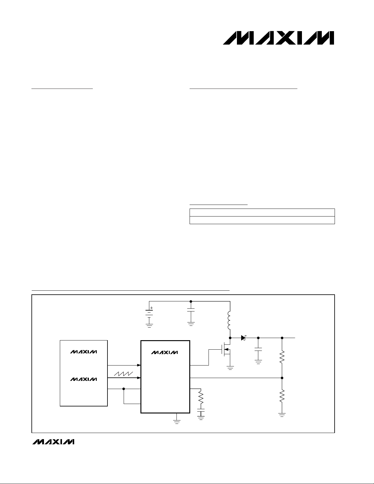
Typical Operating Circuit
19-1741 Rev 0; 10/00
Ordering Information
Pin Configuration appears at end of data sheet.
8 SOT23-8
PIN-PACKAGETEMP. RANGE
-40°C to +85°CMAX1801EKA-T
PART
Digital Still Cameras
Digital Video Cameras
Portable DVD Players
Internet Access Tablets
PDAs
Hand-Held Devices
For price, delivery, and to place orders, please contact Maxim Distribution at 1-888-629-4642,
or visit Maxim’s website at www.maxim-ic.com.
BATTERY
0.7V TO V
OUT
V
OUT
MAX1800
OR
MAX1802
1.25V
2.2V TO 5.5V
REF
OSC
IN
DCON
MAX1801
DL
FB
COMP
GND
Page 2
MAX1801
Digital Camera Step-Up Slave
DC-DC Controller
2 _______________________________________________________________________________________
ABSOLUTE MAXIMUM RATINGS
Stresses beyond those listed under “Absolute Maximum Ratings” may cause permanent damage to the device. These are stress ratings only, and functional
operation of the device at these or any other conditions beyond those indicated in the operational sections of the specifications is not implied. Exposure to
absolute maximum rating conditions for extended periods may affect device reliability.
IN, DCON, REF, OSC, FB to GND.........................-0.3V to +6.0V
DL, COMP to GND.......................................-0.3V to (VIN+ 0.3V)
Continuous Power Dissipation (TA= +70°C)
8-Pin SOT23 (derate 6mW/°C above+70°C)................480mW
Operating Temperature Range ...........................-40°C to +85°C
Junction Temperature......................................................+150°C
Storage Temperature Range. ............................-65°C to +150°C
Lead Temperature (soldering, 10s) .................................+300°C
ELECTRICAL CHARACTERISTICS
(Circuit of Figure 1, VIN= +3.3V, V
DCON
= +1.25V, V
REF
= +1.25V, TA= 0°C to +85°C, unless otherwise noted. Typical values are at
T
A
= +25°C.) (Note 1)
GENERAL
VIN Supply Voltage Operating Range 2.7 5.5 V
VIN Undervoltage Lockout Threshold VIN rising 2.2 2.35 2.5 V
REF Input Range 1.19 1.25 1.31 V
REF Undervoltage Lockout Threshold V
Shutdown Supply Current VIN = 5.5V, V
Sleep-Mode Supply Current VIN = 3.3V, V
Quiescent Supply Current V
OSCILLATOR INPUT
OSC Input Leakage Current V
Oscillator Frequency Range 100 1000 kHz
OSC Clock Low Trip Level 0.20 0.25 0.30 V
OSC Clock High Trip Level
Maximum Duty Cycle Adjustment Range
(Note 2)
Maximum Duty Cycle (Note 2) V
Default Maximum Duty Cycle (Note 2) V
INPUTS/OUTPUTS
DCON Input Leakage Current V
DCON Input Sleep-Mode Threshold IIN ≤ 10µA 0.35 0.4 0.45 V
ERROR AMPLIFIER
FB Regulation Voltage 1.238 1.250 1.263 V
FB to COMP Transconductance -5µA < I
FB to COMP Maximum Voltage Gain 2000 V/V
FB Input Leakage Current VFB = 1.35V 30 100 nA
PARAMETER CONDITIONS MIN TYP MAX UNITS
REF
OSC
OSC
V
DCON
f
OSC
DCON
DCON
DCON
V
DCON
V
DCON
V
DCON
rising 0.9 1.0 1.1 V
= 0, V
DCON
= 0, V
DCON
= 0, V
= 1.5V 0.04 1 µA
= 100kHz 40 90 %
= 0 124 300 µA
FB
= 0.625V 0.575 0.625 0.675
= 0.625V, f
= 1.25V, f
= 5.5V 9 100 nA
= 0 0.5 1.1
= V
= V
COMP
OSC
OSC
REF
, during soft-start 13 30
REF
< 5µA 70 100 160 µS
= 0 0.01 1 µA
REF
= 1.25V 5 10 µA
REF
1.00 1.05 1.10
= 100kHz 50 %
= 100kHz 84 %
3.3 10REF Input Current
V
µA
Page 3
MAX1801
Digital Camera Step-Up Slave
DC-DC Controller
_______________________________________________________________________________________ 3
ELECTRICAL CHARACTERISTICS
(Circuit of Figure 1, VIN= +3.3V, V
DCON
= +1.25V, V
REF
= +1.25V, TA= -40°C to +85°C, unless otherwise noted.) (Note 1)
ELECTRICAL CHARACTERISTICS (continued)
(Circuit of Figure 1, VIN= +3.3V, V
DCON
= +1.25V, V
REF
= +1.25V, TA= 0°C to +85°C, unless otherwise noted. Typical values are at
T
A
= +25°C.) (Note 1)
DRIVER
DL Driver Resistance 2.5 5 Ω
DL Drive Current 0.5 A
SOFT-START
Soft-Start Interval 1024
SHORT-CIRCUIT PROTECTION
Fault Interval 1024
PARAMETER CONDITIONS MIN TYP MAX UNITS
GENERAL
VIN Supply Voltage Operating Range 2.7 5.5 V
VIN Undervoltage Lockout Threshold VIN rising 2.15 2.55 V
REF Input Range 1.19 1.31 V
REF Undervoltage Lockout Threshold V
Shutdown Supply Current VIN = 5.5V, V
Sleep-Mode Supply Current VIN = 3.3V, V
Quiescent Supply Current V
OSCILLATOR INPUT
OSC Input Leakage Current V
Oscillator Frequency Range 100 1000 kHz
OSC Clock Low Trip Level 0.20 0.30 V
OSC Clock High Trip Level
Maximum Duty Cycle Adjustment Range
(Note 2)
INPUTS/OUTPUTS
DCON Input Leakage Current V
DCON Input Sleep-Mode Threshold IIN ≤ 10µA 0.35 0.45 V
PARAMETER CONDITIONS MIN TYP MAX UNITS
V
f
OSC
V
V
V
rising 0.85 1.15 V
REF
= 0, V
DCON
= 0, V
DCON
= 0, V
OSC
= 1.5V 1 µA
OSC
DCON
= 100kHz 40 90 %
DCON
DCON
DCON
DCON
= 0 300 µA
FB
= 0.625V 0.575 0.675
= 5.5V 100 nA
= 0 1.1
= V
REF
= V
, during soft-start 30
REF
= 0 1 µA
REF
= 1.25V 10 µA
REF
1.00 1.10
10REF Input Current
OS C
cycl es
OS C
cycl es
V
µA
Page 4

MAX1801
Digital Camera Step-Up Slave
DC-DC Controller
4 _______________________________________________________________________________________
ELECTRICAL CHARACTERISTICS (continued)
(Circuit of Figure 1, VIN= +3.3V, V
DCON
= +1.25V, V
REF
= +1.25V, TA= -40°C to +85°C, unless otherwise noted.) (Note 1)
Typical Operating Characteristics
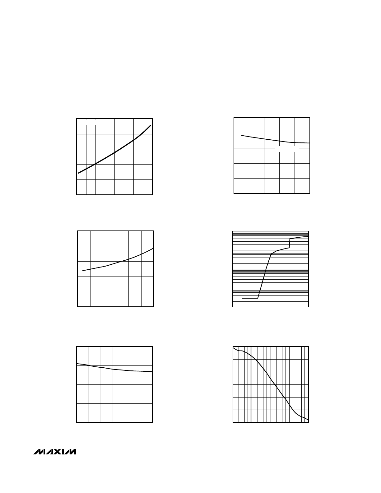
(Circuit of Figure 1, TA = +25°C, unless otherwise noted.)
90
0
1 100010010
EFFICIENCY vs. LOAD CURRENT
30
10
70
50
100
40
20
80
60
MAX1801 toc01
LOAD CURRENT (mA)
EFFICIENCY (%)
V
BATT
= +1.5V
V
OUT
= +12V
V
OUT
= +7V
V
OUT
= +18V
90
0
1 100010010
EFFICIENCY vs. LOAD CURRENT
30
10
70
50
100
40
20
80
60
MAX1801 toc02
LOAD CURRENT (mA)
EFFICIENCY (%)
V
BATT
= +2.4V
V
OUT
= +12V
V
OUT
= +7V
V
OUT
= +18V
90
0
1 100010010
EFFICIENCY vs. LOAD CURRENT
30
10
70
50
100
40
20
80
60
MAX1801 toc03
LOAD CURRENT (mA)
EFFICIENCY (%)
V
BATT
= +3.6V
V
OUT
= +12V
V
OUT
= +18V
V
OUT
= +7V
Note 1: All devices are 100% tested at TA= +25°C. All limits over the temperature range are guaranteed by design.
Note 2: Oscillator signal is generated by the MAX1800 or MAX1802.
PARAMETER CONDITIONS MIN TYP MAX UNITS
ERROR AMPLIFIER
FB Regulation Voltage 1.238 1.263 V
FB to COMP Transconductance -5µA < I
FB Input Leakage Current VFB = 1.35V 100 nA
DRIVER
DL Driver Resistance 5 Ω
< 5µA 70 160 µS
COMP
Page 5
MAX1801
Digital Camera Step-Up Slave
DC-DC Controller
_______________________________________________________________________________________ 5
Typical Operating Characteristics (continued)
(Circuit of Figure 1, TA = +25°C, unless otherwise noted.)
MAXIMUM DUTY CYCLE vs. V
100
f
= 500kHz
OSC
80
60
40
MAXIMUM DUTY CYCLE (%)
20
0
0.4 0.60.5 0.7 0.8 0.9 1.0 1.1 1.2
V
(V)
DCON
SLEEP-MODE CURRENT
vs. INPUT VOLTAGE
10
8
6
4
DCON
MAX1801 toc04
MAX1801toc06
DEFAULT MAXIMUM DUTY CYCLE
vs. FREQUENCY
100
80
60
40
20
DEFAULT MAXIMUM DUTY CYCLE (%)
0
0 400200 600 800 1000
FREQUENCY (kHz)
C
OSC
= 470pF
SHUTDOWN CURRENT
vs. REFERENCE VOLTAGE
10
1
0.1
MAX1801 toc05
MAX1801 toc07
SLEEP-MODE CURRENT (µA)
2
0
2.5 3.53.0 4.0 4.5 5.0 5.5
INPUT VOLTAGE (V)
REFERENCE INPUT CURRENT
vs. TEMPERATURE
3.40
3.35
3.30
3.25
REFERENCE CURRENT (µA)
3.20
-40 0-20 20 40 60 80
TEMPERATURE (°C)
MAX1801 toc08
SHUTDOWN CURRENT (µA)
0.01
0.001
0 0.5 1.0 1.5
REFERENCE VOLTAGE (V)
FB TO COMP SMALL-SIGNAL OPEN-LOOP
FREQUENCY RESPONSE
60
50
40
30
20
SMALL-SIGNAL RESPONSE (dB)
10
0
1 100 100010 10,000
FREQUENCY (kHz)
MAX1801 toc09
Page 6

MAX1801
Digital Camera Step-Up Slave
DC-DC Controller
6 _______________________________________________________________________________________
Pin Description
Typical Operating Characteristics (continued)
(Circuit of Figure 1, TA = +25°C, unless otherwise noted.)
OV
OV
OA
PIN NAME FUNCTION
1 OSC
2 GND Ground
3 REF
4 DCON
STARTUP RESPONSE
1ms/div
Oscillator Input. Connect OSC to OSC of the MAX1800 or MAX1802. The oscillator frequency must
be between 100kHz and 1MHz.
1.25V Reference Input. Connect REF to REF of the MAX1800 or MAX1802. REF must be above 1V
for the controller to turn on. Bypass REF to GND with a 0.1µF or greater capacitor.
Maximum Duty-Cycle Control Input. Connect to REF or IN to set the default maximum duty cycle.
Connect a resistive voltage-divider from REF to DCON to set the maximum duty cycle between 40%
and 90%. Pull DCON below 0.35V to turn the controller off.
MAX1801 toc10
V
DCON
5V/div
V
OUT
2V/div
I
IN
0.5A/div
500mA
100mA
LOAD TRANSIENT RESPONSE
OA
VIN = =+2.4V, V
OUT
= +5V, f
400µs/div
MAX1801 toc11
V
OUT
100mV/div
(AC-COUPLED)
I
LOAD
0.2A/div
= 500kHz
OSC
5 COMP
6 FB
7 IN
8 DL
Controller Compensation. Output of transconductance error amplifier. Connect a series resistor and
capacitor to GND to compensate the control loop. See Compensation Design.
Controller Feedback Input. Connect a feedback resistive voltage-divider from the output to FB to
set the output voltage. Regulation voltage is V
IC Supply Bias Input. Bypass IN to GND with a 0.1µF or greater ceramic capacitor. Supply range is
2.7V to 5.5V.
External MOSFET Gate Drive Output. DL swings between IN and GND with typical 500mA drive
current. Connect DL to the gate of the external switching N-channel MOSFET.
REF
(1.25V).
Page 7

MAX1801
Digital Camera Step-Up Slave
DC-DC Controller
_______________________________________________________________________________________ 7
MAX1800
Figure 1. Typical Application Circuit
Detailed Description
Master-Slave Configuration
The MAX1801 is a step-up slave DC-DC controller that
obtains its input power, voltage reference, and oscillator signal directly from a MAX1800 or MAX1802 master
DC-DC converter (Figure 1). The master-slave configuration reduces system cost by eliminating redundant
circuitry and controls the harmonic content of noise by
synchronizing converter switching.
Step-Up DC-DC Controller
The MAX1801 controller operates in a low-noise fixedfrequency PWM mode, with output power limited by the
external components. The controller regulates the output voltage by modulating the pulse width of the drive
signal for an external N-channel MOSFET switch. The
user-adjusted switching frequency is constant (100kHz
to 1MHz) and set by the master converter.
Figure 2 shows a block diagram of the MAX1801 PWM
controller. A sawtooth oscillator signal from the master
converter (at OSC) governs the internal timing. At the
beginning of each cycle, DL goes high to turn on the
external MOSFET switch. The MOSFET switch turns off
when the internally level-shifted sawtooth waveform
voltage rises above the voltage at COMP or when the
maximum duty cycle is exceeded. The switch remains
off until the beginning of the next cycle. An internal
transconductance amplifier establishes an integrated
error voltage at COMP, increasing the loop gain for
improved regulation accuracy and compensation control.
Reference
The MAX1801 requires a 1.25V reference voltage that
is obtained from the MAX1800 or the MAX1802. REF
typically sinks 0.5µA in shutdown mode, 3µA in active
mode, and up to 30µA during startup. If multiple
MAX1801 controllers are turned on simultaneously,
ensure that the master voltage reference can provide
sufficient current, or buffer the reference with an appropriate unity-gain amplifier.
OR
MAX1802
C
V
BATT
3.3V
1.25V
R3
R4
IN
OSC
REF
DCON
MAX1801
COMP
GND
IN
10µF
DL
FB
R
C
10k
C
C
1000pF
L
2.2µH
MBRO520L
FDN337N
C
OUT
47µF
V
OUT
R1
R2
Page 8

MAX1801
Digital Camera Step-Up Slave
DC-DC Controller
8 _______________________________________________________________________________________
Oscillator
The MAX1801 requires a 0 to 1.25V sawtooth oscillator
signal that is obtained from the MAX1800 or the
MAX1802 (at OSC). The 100kHz to 1MHz oscillator signal sets the converter switching frequency, and it is
used to control pulse-width modulation and maximum
duty cycle.
Maximum Duty Cycle
The MAX1801 uses the master-generated oscillator signal at OSC, the voltage at DCON, and an internal comparator to limit its maximum switching duty cycle (see
Setting the Maximum Duty Cycle). Limiting the duty
cycle can prevent saturation in some magnetic compo-
nents. A low maximum duty cycle can also force the
converter to operate in discontinuous current mode,
simplifying design stability at the cost of a slight reduction in efficiency.
Soft-Start
The MAX1801 features a soft-start function that limits
inrush current and prevents excessive battery loading
at startup by ramping the output voltage to the regulation voltage. This is achieved by increasing the internal
reference to the transconductance amplifier from 0 to
the 1.25V reference voltage over 1024 oscillator cycles
when initial power is applied or when the part is taken
out of shutdown or sleep mode.
Figure 2. PWM Controller Block Diagram
FB
COMP
LEVEL
REFI
REF
SHIFT
SOFT-
START*
R
S
Q
DL
DCON
OSC
*SOFT-START RAMPS REFI FROM 0 TO V
0.4V
1.1V
IN
2.35V
IC
POWER
IN 1024 CLK CYCLES.
REF
CLK
FAULT
PROTECTION
ENABLE
POWER-ON
Page 9

MAX1801
Digital Camera Step-Up Slave
DC-DC Controller
_______________________________________________________________________________________ 9
Shutdown
Set V
DCON
less than 0.35V to place the MAX1801 in
sleep mode, which drops the supply current to 5µA. To
reduce the supply current to 10nA, place the MAX1801
in shutdown by setting V
REF
below 0.4V. The MAX1801
enters soft-start when both V
DCON
and V
REF
are at nor-
mal levels.
Short-Circuit Protection
The MAX1801 has a fault protection feature that prevents damage to transformer-coupled or SEPIC circuits
due to an output short circuit. If the output voltage
drops out of regulation, the voltage at COMP is
clamped at 2.7V. If this condition is maintained for 1024
oscillator clock periods at any time following soft-start,
the MAX1801 is disabled to prevent excessive output
current. Restart the controller by cycling the voltage at
DCON or IN to GND and back to a normal state. For a
step-up application, short-circuit current is not limited,
due to the DC current path through the inductor and
output rectifier to the short circuit. If short-circuit protection is required in a step-up configuration, a protection
device such as a fuse must be used to limit short-circuit
current.
Design Procedure
The MAX1801 can operate in a number of DC-DC converter configurations, including step-up, SEPIC, and flyback. The following design discussions are limited to
the step-up configuration shown in Figure 1; SEPIC and
flyback examples are discussed in the Applications
Information section.
Switching Frequency
The MAX1801 switching frequency is set by the
MAX1800 or MAX1802 master converter (refer to the
appropriate data sheet for the design procedure).
Choose a switching frequency to optimize external
component size or efficiency for the particular
MAX1801 application. Typically, switching frequencies
between 400kHz and 500kHz offer a good balance
between component size and efficiency—higher frequencies generally allow smaller components, and
lower frequencies give better conversion efficiency.
Setting the Output Voltages
Set the MAX1801 output voltage by connecting a resistive voltage-divider from the output to FB as shown in
Figure 1. The FB input bias current is less than 100nA,
so choose R2 to be 100kΩ to minimize the effect of
input bias current at FB. Choose R1 according to the
relation:
where V
FB
is 1.25V, the regulation set point for the
MAX1801.
Setting the Maximum Duty Cycle
The master oscillator signal at OSC and the voltage at
DCON are used to generate the internal clock signal
(CLK in Figure 2). The internal clock’s falling edge
occurs when V
OSC
exceeds V
DCON
, the voltage at
DCON set by a resistive voltage-divider. The internal
clock’s rising edge occurs when V
OSC
falls below
0.25V (Figure 3). The maximum duty cycle can be
approximated by the equation:
where f
OSC
and t
FALL
are the oscillator frequency (in
Hz) and the fall time (typically 100ns), respectively.
At 100kHz, the adjustable maximum duty-cycle range is
typically 28% to 92% (see Maximum Duty Cycle vs.
V
DCON
in the Typical Operating Characteristics). The
maximum duty cycle typically defaults to 78% at 100kHz
if V
DCON
is at or above the voltage at V
REF
(1.25V), and
the controller shuts down if V
DCON
is less than 0.4V. If a
resistive voltage-divider is used at DCON, shut down the
MAX1801 by pulling DCON low with an open-drain signal from an external transistor. Drive DCON with appropriate logic levels to turn the MAX1801 on and off if the
default duty-cycle limit is used.
Figure 3. Setting the Maximum Duty Cycle
(V)
V
OSC
1.25
V
DCON
0.25
0
CLK
t
1
t
2
t
2
D
=
MAX
t1 +
t
2
RR
V
11
=−
OUT
2
V
FB
D
MAX OSC FALL
4
R
=
+
34
RR
−
1
ft
()
Page 10

MAX1801
Digital Camera Step-Up Slave
DC-DC Controller
10 ______________________________________________________________________________________
Inductor Selection
Select the inductor for either continuous or discontinuous
current. Continuous conduction generally is the most efficient. Use discontinuous current if the step-up ratio
(V
OUT
/ VIN) is greater than 1 / ( 1 – D
MAX
).
Continuous Inductor Current
For most MAX1801 step-up designs, a reasonable
inductor value (L
IDEAL
) can be derived from the following equation, which sets continuous peak-to-peak
inductor current at 1/3 the DC inductor current:
where D, the duty cycle, is given by:
In these equations, VSWis the voltage drop across the
N-channel MOSFET switch, and VDis the forward voltage drop across the rectifier. Given L
IDEAL
, the consis-
tent peak-to-peak inductor current is 0.333 I
OUT
/ (1 – D).
The maximum inductor current is 1.167 I
OUT
/ (1 – D).
Inductance values smaller than L
IDEAL
can be used;
however, the maximum inductor current will rise as L is
reduced, and a larger output capacitance will be
required to maintain output ripple.
The inductor current will become discontinuous if I
OUT
decreases by more than a factor of six from the value
used to determine L
IDEAL
.
Discontinuous Inductor Current
In the discontinuous mode of operation, the MAX1801
controller regulates the output voltage by adjusting the
duty cycle to allow adequate power transfer to the load.
To ensure regulation under worst-case load conditions
(maximum I
OUT
), choose:
The peak inductor current is VIND
MAX
/ (L f
OSC
).
The inductor’s saturation current rating should meet or
exceed the calculated peak inductor current.
Input and Output Filter Capacitors
The input capacitor (CIN) in step-up designs reduces
the current peaks drawn from the battery or input
power source and lessens switching noise in the controller. The impedance of the input capacitor at the
switching frequency should be less than that of the
input source so that high-frequency switching currents
do not pass through the input source.
The output capacitor is required to keep the output voltage ripple small and to ensure stability of the regulation
control loop. The output capacitor must have low
impedance at the switching frequency. Tantalum and
ceramic capacitors are good choices. Tantalum capacitors typically have high capacitance and medium-tolow equivalent series resistance (ESR) so that ESR
dominates the impedance at the switching frequency.
In turn, the output ripple is approximately:
V
RIPPLE
≈ I
L(PEAK)
ESR
where I
L(PEAK)
is the peak inductor current.
Ceramic capacitors typically have lower ESR than tantalum capacitors, but with relatively small capacitance
that dominates the impedance at the switching frequency. In turn, the output ripple is approximately:
V
RIPPLE
≈ I
L(PEAK)ZC
where IL(PEAK) is the peak inductor current, and ZC ≈
1 / (2 p fOSC COUT ).
See the Compensation Design section for a discussion
of the influence of output capacitance and ESR on regulation control loop stability.
The capacitor voltage rating must exceed the maximum
applied capacitor voltage. For most tantalum capacitors, manufacturers suggest derating the capacitor by
applying no more than 70% of the rated voltage to the
capacitor. Ceramic capacitors are typically used up to
the voltage rating of the capacitor. Consult the manufacturer’s specifications for proper capacitor derating.
Bypass Capacitors
If the MAX1801 is placed far from the MAX1800 or
MAX1802 master IC, noise from switching circuits can
affect the MAX1801. Should this be the case, bypass
REF and IN with 0.1µF or greater ceramic capacitors. If
noise is not a problem or if the MAX1801 is placed close
to the master IC, then no extra bypassing is required.
MOSFET Selection
The MAX1801 controller drives an external logic-level
N-channel MOSFET as the circuit switch element. The
key selection parameters are as follows:
• On-resistance (R
DS(ON)
)
• Maximum drain-to-source voltage (V
DS(MAX)
)
• Minimum threshold voltage (V
TH(MIN)
)
• Total gate charge (Qg)
• Reverse transfer capacitance (C
RSS
)
L
IDEAL
VV DD
−−31()()
IN SW
=
If
OUT OSC
V
D
≈−+1
IN
VV
OUT D
VD
OUT MAX
L
≤
If
2
OUT OSC
Page 11

MAX1801
Digital Camera Step-Up Slave
DC-DC Controller
______________________________________________________________________________________ 11
Since the external gate drive (DL) swings between IN
and GND, use a MOSFET whose on-resistance is specified at or below VIN. The gate charge, Qg, includes all
capacitance associated with gate charging and helps
to predict the transition time required to drive the MOSFET between on and off states. The power dissipated in
the MOSFET is due to on-resistance and transition losses. The on-resistance loss is:
P1≈ D I
L
2
R
DS(ON)
where D is the duty cycle, ILis the average inductor
current, and R
DS(ON)
is the on-resistance of the MOS-
FET. The transition loss is approximately:
where V
OUT
is the output voltage, ILis the average
inductor current, f
OSC
is the converter switching frequency, and tTis the transition time. The transition time
is approximately Qg/ IG, where Qgis the total gate
charge and IGis the gate drive current (typically 0.5A).
The total power dissipation in the MOSFET is:
P
MOSFET
= P1+ P
2
Diode Selection
For low-output-voltage applications, use a Schottky
diode to rectify the output voltage because of the
diode’s low forward voltage and fast recovery time.
Schottky diodes exhibit significant leakage current at
high reverse voltages and high temperatures. Thus, for
high-voltage, high-temperature applications, use ultrafast junction rectifiers.
Compensation Design
MAX1801 converters use voltage mode to regulate their
output voltages. The following explains how to compensate the control system for optimal performance. The
compensation differs depending on whether the inductor current is continuous or discontinuous.
Discontinuous Inductor Current
For discontinuous inductor current, the PWM converter
has a single pole. The pole frequency and DC gain of
the PWM controller are dependent on the operating
duty cycle, which is:
D = (2 L f
OSC
/ RE)
1/2
where REis the equivalent load resistance, or:
RE= V
IN
2
R
LOAD
/ (V
OUT(VOUT
– VIN))
The frequency of the single pole due to the PWM converter is:
PO= (2 V
OUT
– VIN) / (2 π (V
OUT
– VIN) R
LOADCOUT
)
And the DC gain of the PWM controller is:
AVO= 2 V
OUT(VOUT
– VIN) R
LOAD
/ ((2 V
OUT
– VIN) D)
Note that the pole frequency decreases and the DC
gain increases proportionally as the load resistance
(RLOAD) is increased. Since the crossover frequency
is the product of the pole frequency and the DC gain, it
remains independent of the load.
The gain through the voltage-divider is:
A
VDV
= V
REF
/ V
OUT
And the DC gain of the error amplifier is A
VEA
= 2000V/V.
Thus, the DC loop gain is:
A
VDC
= A
VDVAVEAAVO
The compensation resistor-capacitor pair at COMP cause
a pole and zero at frequencies (in Hz):
PC= GEA/ (4000 π CC) = 1 / (4 x 10
7
π C
C
)
ZC= 1 / (2 π RCCC)
And the ESR of the output filter capacitor causes a zero
in the loop response at the frequency (in Hz):
ZO= 1 / (2π C
OUT
ESR)
The DC gain and the poles and zeros are shown in the
Bode plot of Figure 4.
To achieve a stable circuit with the Bode plot of Figure
4, perform the following procedure:
Figure 4. MAX1801 Discontinuous-Current, Voltage-Mode,
Step-Up Converter Bode Plot
VIft
OUT L OSC T
P
23≈
180°
90°
PHASE
0°
GAIN
(dB)
80
P
A
VDC
60
40
20
O
-20
C
PHASE
ZC = P
O
GAIN
Z
O
FREQUENCY
Page 12

MAX1801
Digital Camera Step-Up Slave
DC-DC Controller
12 ______________________________________________________________________________________
1) Choose the compensation resistor RCthat is equivalent to the inverse of the transconductance of the
error amplifier, 1/ RC= GEA= 100µS, or RC= 10kΩ.
This sets the high-frequency voltage gain of the
error amplifier to 0dB.
2) Determine the maximum output pole frequency:
where:
R
LOAD(MIN)
= V
OUT
/ I
OUT(MAX)
3) Place the compensation zero at the same frequency
as the maximum output pole frequency (in Hz):
Solving for C
C
:
Use values of C
C
less than 10nF. If the above calculation determines that the capacitor should be
greater than 10nF, use C
C
= 10nF, skip step 4 , and
proceed to step 5.
4) Determine the crossover frequency (in Hz):
fC= V
REF
/ (π D C
OUT
)
and to maintain at least a 10dB gain margin, make
sure that the crossover frequency is less than or
equal to 1/3 of the ESR zero frequency, or:
3fC≤ Z
O
or:
ESR ≤ D / 6 V
REF
If this is not the case, go to step 5 to reduce the
error amplifier high-frequency gain to decrease the
crossover frequency.
5) The high-frequency gain may be reduced, thus
reducing the crossover frequency, as long as the
zero due to the compensation network remains at or
below the crossover frequency. In this case:
ESR ≤ D / (GEARC6 V
REF
)
and:
f
C
= (GEARC) 2 V
REF
/ (2π DC
OUT
) ≥ 1 / (2π RCCC)
Choose C
OUT
, RC, and CCto simultaneously satisfy
both equations.
Continuous Inductor Current
For continuous inductor current, there are two conditions that change, requiring different compensation.
The response of the control loop includes a right-halfplane zero and a complex pole pair due to the inductor
and output capacitor. For stable operation, the controller loop gain must drop below unity (0dB) at a much
lower frequency than the right-half-plane zero frequency. The zero arising from the ESR of the output capacitor is typically used to compensate the control circuit
by increasing the phase near the crossover frequency,
increasing the phase margin. If a low-value, low-ESR
output capacitor (such as a ceramic capacitor) is used,
the ESR-related zero occurs at too high a frequency
and does not increase the phase margin. In this case,
use a lower value inductor so that it operates with discontinuous current (see the Discontinuous Inductor
Current section).
For continuous inductor current, the gain of the voltage
divider is A
VDV
= V
REF
/ V
OUT
, and the DC gain of the
error amplifier is A
VEA
= 2000. The gain through the
PWM controller in continuous current is:
AVO= (1 / V
REF
) (V
OUT
2
/ VIN)
Thus, the total DC loop gain is:
A
VDC
= 2000 V
OUT
/ V
IN
The complex pole pair due to the inductor and output
capacitor occurs at the frequency (in Hz):
PO= (V
OUT
/ VIN) / (2π (L × C
OUT
)
1/2
)
The pole and zero due to the compensation network at
COMP occur at the frequencies (in Hz):
PC = GEA/ (4000 π CC) = 1 / (4 x 10
7
π C
C
)
ZC= 1 / (2π RCCC)
The frequency (in Hz) of the zero due to the ESR of the
output capacitor is:
ZO= 1 / (2π C
OUT
ESR)
And the right-half-plane zero frequency (in Hz) is:
The Bode plot of the loop gain of this control circuit is
shown in Figure 5.
P
O(MAX)
=
2V - V
V-V C
IN LOAD(MIN)
OUT OUT
OUT
R2π()
IN
Z
C
CC V
12V-V
==
22ππRC R()
CC
=
C OUT OUT
V-V C
OUT IN LOAD(MIN) OUT
R()2
C OUT(MAX) OUT IN
OUT IN
V-V
OUT IN
IV-V
2
Z
RHP
(1- D) R
=
2L
π
LOAD
Page 13

MAX1801
Digital Camera Step-Up Slave
DC-DC Controller
______________________________________________________________________________________ 13
To configure the compensation network for a stable
control loop, set the crossover frequency at that of the
zero due to the output capacitor ESR. Use the following
procedure:
1) Determine the frequency of the right-half-plane
zero:
2) Find the DC loop gain:
A
VDC
= 2000 V
OUTVIN
3) Determine the frequency of the complex pole pair
due to the inductor and output capacitor:
f
O
= (V
OUT
/ VIN) / (2π (L C
OUT
)
1/2
)
4) Since response is 2nd order (-40dB per decade)
between the complex pole pair and the ESR zero,
determine the desired amplitude at the complex
pole pair to force the crossover frequency equal to
the ESR zero frequency. Thus:
A(P
O
) = (ZO/ PO)2= L V
IN
2
/ (C
OUT
ESR2V
OUT
2
)
5) Determine the desired compensation pole. Since
the response between the compensation pole and
the complex pole pair is 1st order (-20dB per
decade), the ratio of the frequencies is equal to the
ratio of the amplitudes at those frequencies. Thus:
(P
O
/ PC) = (ADC/ A(PO))
Solving this equation for CC:
CC= V
OUT(COUT
)
3/2
ESR2/ (20MΩ VIN(L)
1/2
)
6) Determine that the compensation resistor, RCfor
the compensation zero frequency, is equal to the
complex pole-pair frequency:
Z
C
= P
O
solving for RC:
R
C
= (VIN/ V
OUT
) ((L C
OUT
)
1/2
/ CC)
Applications Information
Using the MAX1801 with the MAX1800
Step-Up Master DC-DC Converter
The MAX1801 does not generate its own reference or
oscillator. Instead it uses the reference and the oscillator
from a master DC-DC converter such as the MAX1800
step-up master converter. The MAX1800 has circuitry to
generate a 1.25V reference and a 100kHz to 1MHz oscillator signal. The MAX1800 operates from a 1.5V to 5.5V
input voltage, which makes it suitable for applications
with 2- or 3-cell alkaline, NiCd, or NiMH batteries, or 1-cell
lithium primary or lithium-ion (Li+) batteries. Apart from
the reference and the oscillator, the MAX1800 has a single-internal-switch synchronous-rectified step-up DC-DC
converter, three auxiliary step-up DC-DC converter controllers, and a linear regulator controller. For more details,
refer to the MAX1800 data sheet
Using the MAX1801 with the MAX1802
Step-Down Master DC-DC Converter
The MAX1801 does not generate its own reference or
oscillator. Instead, it uses the reference and the oscillator from a master DC-DC converter such as the
MAX1802 step-down master DC-DC converter. The
MAX1802 has circuitry to generate a 1.25V reference
and a 100kHz to 1MHz oscillator signal. The MAX1802
operates from a 2.7V to 11V input voltage, making it
suitable for 4-series alkaline, NiCd, or NiMH cells, or 2series lithium primary or (Li+) batteries. The MAX1802
has a synchronous-rectified step-down DC-DC converter controller, an internal-switch synchronous-rectified
step-down DC-DC converter, and three auxiliary stepup DC-DC converter controllers. For more details, refer
to the MAX1802 data sheet.
Figure 5. MAX1801 Continuous-Current, Voltage-Mode,
Step-Up Converter Bode Plot
PC
A
VDC
PHASE
GAIN
(dB)
O dB
GAIN
PHASE
MARGIN
FREQUENCY
ZC=P
O
GAIN
Z
0
MARGIN
Z
rRHP
180°
90°
PHASE
0°
Z
RHP
=
2
(1- D) R
2L
π
LOAD
Page 14

MAX1801
Digital Camera Step-Up Slave
DC-DC Controller
14 ______________________________________________________________________________________
Using the MAX1801 Controller in
SEPIC Configuration
In cases where the battery voltage is above or below
the required output voltage, neither a step-up nor a
step-down converter is suitable; use a step-up/stepdown converter instead. One type of step-up/stepdown converter is the SEPIC shown in Figure 6.
Inductors L1 and L2 can be separate inductors or can
be wound on a single core and coupled as with a transformer. Typically, using a coupled inductor improves
efficiency because some power is transferred through
the coupling so that less power passes through the coupling capacitor, C2. Likewise, C2 should be a low-ESRtype capacitor to improve efficiency. The coupling
capacitor ripple current rating must be greater than the
larger of the input and output currents. The MOSFET
(Q1) drain-source voltage rating and the rectifier (D1)
reverse voltage rating must exceed the sum of the input
and output voltages. Other types of step-up/step-down
circuits are a flyback converter and a step-up converter
followed by a linear regulator.
Using the MAX1801 Controller for a
Multi-Output Flyback Circuit
Some applications require multiple voltages from a single converter that features a flyback transformer.
Figure 7 shows a MAX1801 auxiliary controller in a twooutput flyback configuration. The controller drives an
external MOSFET that switches the transformer primary,
and the two secondaries generate the outputs. Only a
single positive output voltage can be regulated using
the feedback resistive voltage-divider, so the other voltages are set by the turns ratio of the transformer secondaries. The regulation of the other secondary voltages
degrades due to transformer leakage inductance and
winding resistance. Voltage regulation is best when the
load current is limited to a small range. Consult the
transformer manufacturer for the proper design for a
given application.
Using a Charge Pump to Make
Negative Output Voltages
Negative output voltages can be produced without a
transformer using a charge-pump circuit with an auxiliary controller, as shown in Figure 8. When MOSFET Q1
turns off, the voltage at its drain rises to supply current
to V
OUT
+. At the same time, C1 charges to the voltage
at V
OUT
+ through D1. When the MOSFET turns on, C1
discharges through D3, thereby charging C3 to V
OUT
minus the drop across D3, to create roughly the same
voltage as V
OUT
+ at V
OUT
- but with inverted polarity. If
different magnitudes are required for the positive and
negative voltages, a linear regulator can be used at one
of the outputs to achieve the desired voltages, while the
MAX1801 regulates the higher magnitude voltage.
Figure 6. MAX1801 Auxiliary Controller, SEPIC Configuration
Figure 7. MAX1801 Auxiliary Controller, Flyback Configuration
INPUT
1 CELL
Li+
L
MAIN
ON
DCON
MAX1801
COMP
INPUT
MAIN
ON
MAX1801
COMP
R
G
DCON
R
G
EXT
C
C
EXT
C
C
FB
Q
FB
2
OUTPUT
R
R
R
1
R
2
3.3V
1
2
+ OUTPUT
- OUTPUT
D
C
Q
1
2
1
D
3
D
2
1
Page 15

MAX1801
Digital Camera Step-Up Slave
DC-DC Controller
______________________________________________________________________________________ 15
Chip Information
TRANSISTOR COUNT: 1130
Pin Configuration
Designing a PC Board
A good PC board layout is important to achieve optimal
performance from the MAX1801. Poor design can cause
excessive conducted and/or radiated noise, both of
which can cause instability and/or regulation errors.
Conductors carrying discontinuous currents should be
kept as short as possible, and conductors carrying
high currents should be made as wide as possible. A
separate low-noise ground plane containing the reference and signal grounds should connect only to the
power-ground plane at one point to minimize the
effects of power-ground currents.
Keep the voltage feedback network very close to the
IC, preferably within 0.2in (5mm) of the FB pin. Nodes
with high dv/dt (switching nodes) should be kept as
small as possible and should be kept away from highimpedance nodes such as FB.
Circuit-board layouts that are susceptible to electrical
noise can require a lowpass RC filter at OSC and
bypassing at REF and IN. If an RC filter is used at OSC,
the pole frequency should be at least 20 times larger
than the oscillator frequency to prevent distortion of the
OSC signal. To ensure minimal loading of the master
oscillator, which would cause an oscillator frequency
shift, choose a filter capacitor smaller than C
OSC
/(100
N), where C
OSC
is the timing capacitor for the master
oscillator and N is the number of MAX1801 slaves connected to the master. Then choose R
FILTER
= 1/(40 π
f
OSCCFILTER
).
If bypass capacitors are required on IN and REF, use
0.1µF ceramic capacitors because of their low impedance at high frequencies. The bypass and filter components should be placed within 5mm (0.2in) of the
MAX1801 pins.
Refer to the MAX1800 evaluation kit (EV kit) or
MAX1802 EV kit data sheets for full PC board examples.
Figure 8. Auxiliary Controller, Charge-Pump Configuration
D
3
V
-
INPUT
C
3
D
MAIN
ON
MAX1801
COMP
DCON
R
G
EXT
C
C
L
FB
C
Q
1
1
1
D
2
C
2
OUT
V
+
OUT
R
1
R
2
TOP VIEW
OSC
1
2
REF
MAX1801
3
4
SOT23-8
87DL
6
5
INGND
FB
COMPDCON
Page 16

MAX1801
Digital Camera Step-Up Slave
DC-DC Controller
Maxim cannot assume responsibility for use of any circuitry other than circuitry entirely embodied in a Maxim product. No circuit patent licenses are
implied. Maxim reserves the right to change the circuitry and specifications without notice at any time.
16 ____________________Maxim Integrated Products, 120 San Gabriel Drive, Sunnyvale, CA 94086 408-737-7600
© 2000 Maxim Integrated Products Printed USA is a registered trademark of Maxim Integrated Products.
Package Information
SOT23, 8L.EPS
 Loading...