

Page 1
General Description
The MAX1775 is a dual, step-down DC-DC converter
that generates both the main (+3.3V at over 2A) and
core (+1.8V at up to 1.5A) supplies for a complete
power solution for PDAs, subnotebooks, and other
hand-held devices. The main output is adjustable from
+1.25V to +5.5V. The core output is adjustable from 1V
to 5V. Both switching converters operate at up to
1.25MHz for small external components and use synchronous rectifiers to achieve efficiencies up to 95%.
Operation with up to 100% duty cycle provides the lowest possible dropout voltage to extend useful battery
life.
The MAX1775 accepts inputs from +2.7V up to +28V,
allowing use with many popular battery configurations as
well as AC-DC wall adapters. Digital soft-start reduces
battery current surges at power-up. Both the main and
core converters have separate shutdown inputs. The
MAX1775 comes in a small 16-pin QSOP package.
The MAX1775 evaluation kit is available to help reduce
design time.
________________________Applications
Hand-Held Computers
PDAs
Internet Access Tablets
POS Terminals
Subnotebooks
Features
♦ Dual, High-Efficiency, Synchronous Rectified
Step-Down Converter
♦ Main Power
Adjustable from +1.25V to +5.5V
Over 2A Load Current
Up to 95% Efficiency
♦ Core Power
Adjustable from 1V to 5V
Internal Switches
Up to 1.5A Load Current
Up to 92% Efficiency
♦ 100% (max) Duty Cycle
♦ Up to 1.25MHz Switching Frequency
♦ Input Voltage Range from +2.7V to +28V
♦ 170µA Quiescent Current
♦ 5µA Shutdown Current
♦ Digital Soft-Start
♦ Independent Shutdown Inputs
MAX1775
Dual-Output Step-Down
DC-DC Converter for PDA/Palmtop Computers
________________________________________________________________ Maxim Integrated Products 1
Pin Configuration
19-1811; Rev 1; 8/01
EVA
LUA
TIO
N
KIT
AVA
ILA
B
LE
Ordering Information
Typical Operating Circuit
For pricing, delivery, and ordering information, please contact Maxim/Dallas Direct! at
1-888-629-4642, or visit Maxim’s website at www.maxim-ic.com.
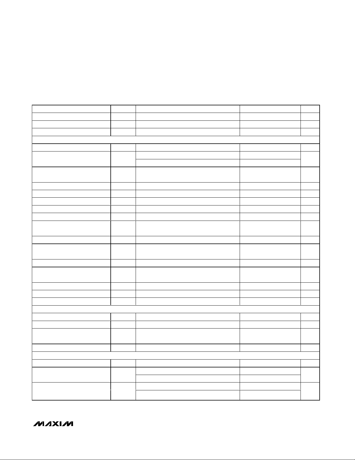
PART TEMP. RANGE PIN-PACKAGE
MAX1775EEE -40°C to +85°C 16 QSOP
IN 2.7V TO 5.5V (28V IN CASCADE)
IN
CVH
MAX1775
INC
PDRV
NDRV
CS+
CS-
FBM
LXC
FBC
CORE
1.8V
1.5A
TOP VIEW
ON
OFF
OFF
SHDNM
SHDNC
CVL
REF
PGND
GND
ON
1
SHDNM LXC
2
SHDNC
PGND
3
MAX1775
4
NDRV
CVL
5
IN
6
PDRV
7
CVH
8
16 QSOP
16
15
INC
14
GND
13
FBC
12
CS-
CS+
11
10
FBM
9
REF
MAIN
3.3V
OVER 2A
Page 2
MAX1775
Dual-Output Step-Down
DC-DC Converter for PDA/Palmtop Computers
2 _______________________________________________________________________________________
ABSOLUTE MAXIMUM RATINGS
ELECTRICAL CHARACTERISTICS
(VIN= +12V, V
MAIN
= V
INC
= V
CS-
= V
CS+
= +3.3V, V
CORE
= +1.8V, Circuit of Figure 4, TA= 0°C to +85°C, unless otherwise noted.
Typical values are at T
A
= +25°C.)
Stresses beyond those listed under “Absolute Maximum Ratings” may cause permanent damage to the device. These are stress ratings only, and functional
operation of the device at these or any other conditions beyond those indicated in the operational sections of the specifications is not implied. Exposure to
absolute maximum rating conditions for extended periods may affect device reliability.
IN, SHDNM, CVH to GND.......................................-0.3V to +30V
IN to CVH, PDRV ......................................................-0.3V to +6V
PDRV to GND..................................(V
CVH
- 0.3V) to (VIN+ 0.3V)
PGND to GND .......................................................-0.3V to +0.3V
All Other Pins to GND...............................................-0.3V to +6V
Core Output Short Circuit...........................................Continuous
Continuous Power Dissipation
16-Pin QSOP (derate 7.1mW/°C above +70°C)..........571mW
Operating Temperature .......................................-40°C to +85°C
Storage Temperature.........................................-65°C to +150°C
Lead Temperature (soldering, 10s) .................................+300°C
(
PARAMETER SYMBOL CONDITIONS MIN TYP MAX UNITS
Input Voltage V
Input Quiescent Supply Current I
CS- Quiescent Supply Current ICS-
Core Regulator Quiescent
Supply Current
IN Shutdown Supply Current SHDNM = SHDNC = GND 5 30 µA
MAIN REGULATOR
Main Output Voltage Adjust
Range
FBM Regulation Threshold V
FBM Input Current I
Current-Limit Threshold V
Minimum Current-Limit
Threshold
Valley Current Threshold V
Zero Current Threshold V
PDRV, NDRV Gate Drive
Resistance
CS- to CVL Switch Resistance I
PDRV, NDRV Dead Time 50 ns
Maximum Duty Cycle 100 %
Minimum On-Time 200 400 650 ns
Minimum Off-Time 200 400 650 ns
IN
IN
I
INC
FBM
FBM
CLM
V
MIN
VALLEYVCS+
ZERO
V
= +1.5V, V
FBM
V
V
V
V
V
V
V
V
V
V
V
= V
SHDNM
= +1.5V, V
FBM
= V
SHDNM
= +1.5V, V
FBM
= V
SHDNM
C S + - C S - )
FBM
CS+
CS+
CS+
CS-
CVL
= 0 to + 60m V , V
= +1.3V -0.1 0.1 µA
- V
CS-
- V
CS-
- V
CS-
- V
CS-
= +3.3V, I
= 50mA 4.5 8 Ω
2.7 28 V
= +1.5V,
FBC
SHDNC
FBC
SHDNC
FBC
SHDNC
= +3.3V
= +1.5V,
= +3.3V
= +1.5V,
= +3.3V
15 30 µA
110 220 µA
60 120 µA
1.25 5.5 V
= + 2.7V to + 28V 1.21 1.25 1.29 V
IN
60 80 100 mV
61524mV
40 50 60 mV
015mV
= 50mA 2 4.4 Ω
LOAD
Page 3
MAX1775
Dual-Output Step-Down
DC-DC Converter for PDA/Palmtop Computers
_______________________________________________________________________________________ 3
ELECTRICAL CHARACTERISTICS (continued)
(VIN= +12V, V
MAIN
= V
INC
= V
CS-
= V
CS+
= +3.3V, V
CORE
= +1.8V, Circuit of Figure 4, TA= 0°C to +85°C, unless otherwise noted.
Typical values are at T
A
= +25°C.)
PARAMETER SYMBOL CONDITIONS MIN TYP MAX UNITS
CORE REGULATOR
Input Voltage Range V
INC Undervoltage Lockout
Core Output Voltage Adjust
Range
Maximum Core Load Current (Note 1) 1 1.5 A
FBC Regulation Threshold V
FBC Input Current I
Dropout Voltage (INC to LXC) I
LXC Leakage Current I
LXC P-Channel, N-Channel
On-Resistance
LXC P-Channel Current Limit I
LXC P-Channel Minimum
Current
LXC N-Channel Valley Current 900 1400 2400 mA
LXC N-Channel Zero-Crossing
Current
LXC Dead Time 50 ns
Maximum Duty Cycle 100 %
Minimum On-Time 170 400 670 ns
Minimum Off-Time 170 400 670 ns
REFERENCE
Reference Voltage V
Reference Load Regulation I
Reference Line Regulation VCS- = +2.5V to +5.5V, I
Reference Sink Current I
CVL, CVH REGULATORS
CVL Output Voltage V
CVL Switchover Threshold V
CVH Output Voltage V
CVH Switchover Threshold V
CVL Undervoltage Lockout
INC
FBC
FBC
LXC
CLC
REF
REF
CVL
CVH
IN
2.6 5.5 V
V
rising 2.40 2.47 2.55
INC
falling 2.30 2.37 2.45
V
INC
1.0 5.0 V
V
= +2.5 to +5.5V, I
INC
V
= +1.3V -0.1 0.1 µA
FBC
= 400mA 0.1 0.25 V
OUTC
V
= +5.5V, V
INC
= 0 to +5.5V -10 10 µA
LXC
= 0 to 200mA 0.97 1.0 1.03 V
OUTC
0.25 0.5 Ω
1200 1800 3000 mA
100 200 400 mA
40 110 170 mA
1.23 1.25 1.27 V
= 0 to 50µA 10 mV
REF
= 50µA 5 mV
REF
10 µA
I
= 50mA, V
CVL
I
= 50mA, VCS- = +3.3V 3.2
CVL
rising, hysteresis = 100mV (typ) 2.40 2.47 2.55 V
CS-
VIN = +4V, I
VIN = +12V, I
= +2.7V, VCS- = 0 2.6 2.8 3.1
IN
= 25mA V
CVH
= 50mA V
CVH
IN
IN
- 3.4 V
- 4.3 V
VIN rising, hysteresis = 350mV (typ) 5.5 V
V
rising 2.40 2.47 2.55
CVL
falling 2.30 2.37 2.45
V
CVL
IN
IN
- 2.8
- 3.7
V
V
V
V
Page 4
MAX1775
Dual-Output Step-Down
DC-DC Converter for PDA/Palmtop Computers
4 _______________________________________________________________________________________
ELECTRICAL CHARACTERISTICS (continued)
(VIN= +12V, V
MAIN
= V
INC
= V
CS-
= V
CS+
= +3.3V, V
CORE
= +1.8V, Circuit of Figure 4, TA= 0°C to +85°C, unless otherwise noted.
Typical values are at T
A
= +25°C.)
ELECTRICAL CHARACTERISTICS
(VIN= +12V, V
MAIN
= V
INC
= V
CS-
= V
CS+
= +3.3V, V
CORE
= +1.8V, Circuit of Figure 4, TA-40°C to +85°C, unless otherwise noted.)
(Note 2)
(
PARAMETER SYMBOL CONDITIONS MIN TYP MAX UNITS
LOGIC INPUTS
SHDNM, SHDNC Input Low
Voltage
SHDNM, SHDNC Input High
Voltage
SHDNM, SHDNC Input Low
Current
SHDNC Input High Current V
SHDNM Input High Current
PARAMETER SYMBOL CONDITIONS MIN MAX UNITS
Input Voltage V
Input Quiescent Supply Current I
CS- Quiescent Supply Current I
Core Regulator Quiescent
Supply Current
IN Shutdown Supply Current SHDNM = SHDNC = GND 30 µA
MAIN REGULATOR
Main Output Voltage Adjust
Range
CS-
I
INC
IN
IN
2.0 V
SHDNM = SHDNC = GND -1 1 µA
= +5.5V 5 µA
SHDNC
V
V
= +5V 2
SHDNM
= +28V 15 30
SHDNM
2.7 28 V
V
FBM
V
SHDNM
V
FBM
V
SHDNM
V
FBM
V
SHDNM
= +1.5V, V
= V
= +1.5V, V
= V
= +1.5V, V
= V
FBC
SHDNC
FBC
SHDNC
FBC
SHDNC
= +1.5V,
= +3.3V
= +1.5V,
= +3.3V
= +1.5V,
= +3.3V
1.25 5.5 V
0.4 V
µA
30 µA
220 µA
120 µA
FBM Regulation Threshold V
FBM Input Current I
FBM
FBM
Current-Limit Threshold V
M i ni m um C ur r ent- Li m i t Thr eshol d V
Valley Current Threshold V
Zero Current Threshold V
PDRV, NDRV Gate Drive
Resistance
CS- to CVL Switch Resistance I
CL
V
C S + - C S - )
V
FBM
V
CS+
CS+
CS+
CS+
V
CS-
CVL
= 0 to + 60m V , V
= + 2.7V to + 28V 1.21 1.29 V
I N
= +1.3V -0.1 0.1 µA
- V
- V
- V
- V
CS-
CS-
CS-
CS-
60 100 mV
624mV
40 60 mV
015mV
= +3.3V 4.4 Ω
= 50mA 8 Ω
Page 5
MAX1775
Dual-Output Step-Down
DC-DC Converter for PDA/Palmtop Computers
_______________________________________________________________________________________ 5
ELECTRICAL CHARACTERISTICS (continued)
(VIN= +12V, V
MAIN
= V
INC
= V
CS-
= V
CS+
= +3.3V, V
CORE
= +1.8V, Circuit of Figure 4, TA-40°C to +85°C, unless otherwise noted.)
(Note 2)
PARAMETER SYMBOL CONDITIONS MIN MAX UNITS
Maximum Duty Cycle 100 %
Minimum On-Time 200 650 ns
Minimum Off-Time 200 650 ns
CORE REGULATOR
Input Voltage Range V
INC Undervoltage Lockout
Core Output Voltage Adjust
Range
Maximum Core Load Current (Note 1) 1 A
FBC Regulation Threshold V
FBC Input Current I
Dropout Voltage (INC to LXC) I
LXC Leakage Current I
LXC P-Channel, N-Channel
On-Resistance
LXC P-Channel Current Limit 1200 3050 mA
LXC P-Channel Minimum
Current
LXC N-Channel Valley Current 880 2450 mA
LXC N-Channel Zero-Crossing
Current
Maximum Duty Cycle 100 %
Minimum On-Time 150 670 ns
Minimum Off-Time 150 670 ns
REFERENCE
Reference Voltage V
Reference Load Regulation I
Reference Line Regulation
Reference Sink Current I
CVL, CVH REGULATORS
CVL Output Voltage V
CVH Output Voltage V
CVL Undervoltage Lockout
INC
FBC
FBC
LXC
REF
REF
CVL
CVH
V
INC
V
INC
V
INC
V
FBC
OUTC
V
INC
REF
V
CS-
I
REF
I
CVL
VIN = +4V, I
VIN = +12V, I
V
CVL
V
CVL
2.6 5.5 V
rising 2.39 2.55
falling 2.29 2.45
1.0 5.0 V
= +2.5V to +5.5V, I
= 0 to 200mA 0.97 1.03 V
OUTC
= +1.3V -0.1 0.1 µA
= 400mA 0.2 V
= +5.5V, V
= 0 to +5.5V -10 10 µA
LXC
0.5 Ω
100 400 mA
35 175 mA
1.22 1.27 V
= 0 to 50µA 10 mV
= +2.5V to +5.5V,
= 50µA
5mV
10 µA
= 50mA, V
= +2.7V, V
IN
= 25mA V
CVH
= 50mA VIN - 3.7
CVH
= 0 2.6 3.1 V
CS-
IN
- 2.8
rising 2.40 2.55
falling 2.30 2.45
V
V
V
Page 6

100
0
1 10 100 1000 10,000
MAIN OUTPUT EFFICIENCY vs. LOAD
20
MAX1775 toc01
LOAD (mA)
EFFICIENCY (%)
40
60
80
70
50
30
10
90
VIN = +12V
VIN = +15V
VIN = +18V
VIN = +5V
VIN = +3.3V
90
0
1 100010010
CORE OUTPUT EFFICIENCY vs. LOAD
30
10
70
50
100
40
20
80
60
MAX1775 toc02
LOAD (mA)
EFFICIENCY (%)
V
INC
= +3.3V
V
INC
= +5V
V
INC
= +2.7V
-2.0
-1.5
-1.0
-0.5
0
0.5
1.0
1.5
2.0
-40 -15 10 35 60 85
V
REF
ACCURACY vs. TEMPERATURE
MAX1775 toc03
TEMPERATURE (°C)
V
REF
ACCURACY (%)
Typical Operating Characteristics
(Circuit of Figure 1, V
MAIN
= +3.3V, V
CORE
= +1.8V, TA = +25°C, unless otherwise noted.)
MAX1775
Dual-Output Step-Down
DC-DC Converter for PDA/Palmtop Computers
6 _______________________________________________________________________________________
ELECTRICAL CHARACTERISTICS (continued)
(VIN= +12V, V
MAIN
= V
INC
= V
CS-
= V
CS+
= +3.3V, V
CORE
= +1.8V, Circuit of Figure 4, TA-40°C to +85°C, unless otherwise noted.)
(Note 2)
Note 1: This parameter is guaranteed based on the LXC P-channel current limit and the LXC N-channel valley current.
Note 2: Specifications to -40°C are guaranteed by design and not production tested.
PARAMETER SYMBOL CONDITIONS MIN MAX UNITS
LOGIC INPUTS
SHDNM, SHDNC Input Low
Voltage
SHDNM, SHDNC Input High
Voltage
SHDNM, SHDNC Input Low
Current
SHDNC Input High Current V
SHDNM Input High Current V
2.0 V
SHDNM = SHDNC = GND -1 1 µA
= +5.5V 5 µA
SHDNC
= +28V 30 µA
SHDNM
0.4 V
Page 7

MAX1775
Dual-Output Step-Down
DC-DC Converter for PDA/Palmtop Computers
_______________________________________________________________________________________ 7
Typical Operating Characteristics (continued)
(Circuit of Figure 1, V
MAIN
= +3.3V, V
CORE
= +1.8V, TA = +25°C, unless otherwise noted.)
-0.2
-0.4
-0.6
-0.8
-1.0
-1.2
ACCURACY (%)
REF
-1.4
V
-1.6
-1.8
-2.0
REFERENCE LOAD REGULATION
0
0203010 40 50 60 70 80
MAIN SWITCHING WAVEFORMS,
HEAVY LOAD (1A)
I
(µA)
REF
MAX1775 toc06
MAX1775 toc04
LX
5V/div
MAIN SWITCHING WAVEFORMS,
LIGHT LOAD (100mA)
1µs/div
MAX1775 toc05
CORE SWITCHING WAVEFORMS,
LIGHT LOAD (50mA)
MAX1775 toc07
LX
5V/div
I
LM
500mA/div
V
MAIN
(AC-COUPLED)
20mV/div
LX
5V/div
1000mA
I
LM
500mA/div
1µs/div
CORE SWITCHING WAVEFORMS,
HEAVY LOAD (500mA)
2µs/div
MAX1775 toc08
500mA
0
V
MAIN
(AC-COUPLED)
20mV/div
4V
LXC
2V/div
0
V
CORE
(AC-COUPLED)
20mV/div
500mA
I
LC
250mA/div
0
1µs/div
MAIN LINE-TRANSIENT RESPONSE
(5V TO 12V)
100µs/div
MAX1775 toc09
200mA
I
LC
200mA/div
0
V
CORE
(AC-COUPLED)
20mV/div
12V
V
IN
5V
0
V
MAIN
50mV/div
Page 8
MAX1775
Dual-Output Step-Down
DC-DC Converter for PDA/Palmtop Computers
8 _______________________________________________________________________________________
Typical Operating Characteristics (continued)
(Circuit of Figure 1, V
MAIN
= +3.3V, V
CORE
= +1.8V, TA = +25°C, unless otherwise noted.)
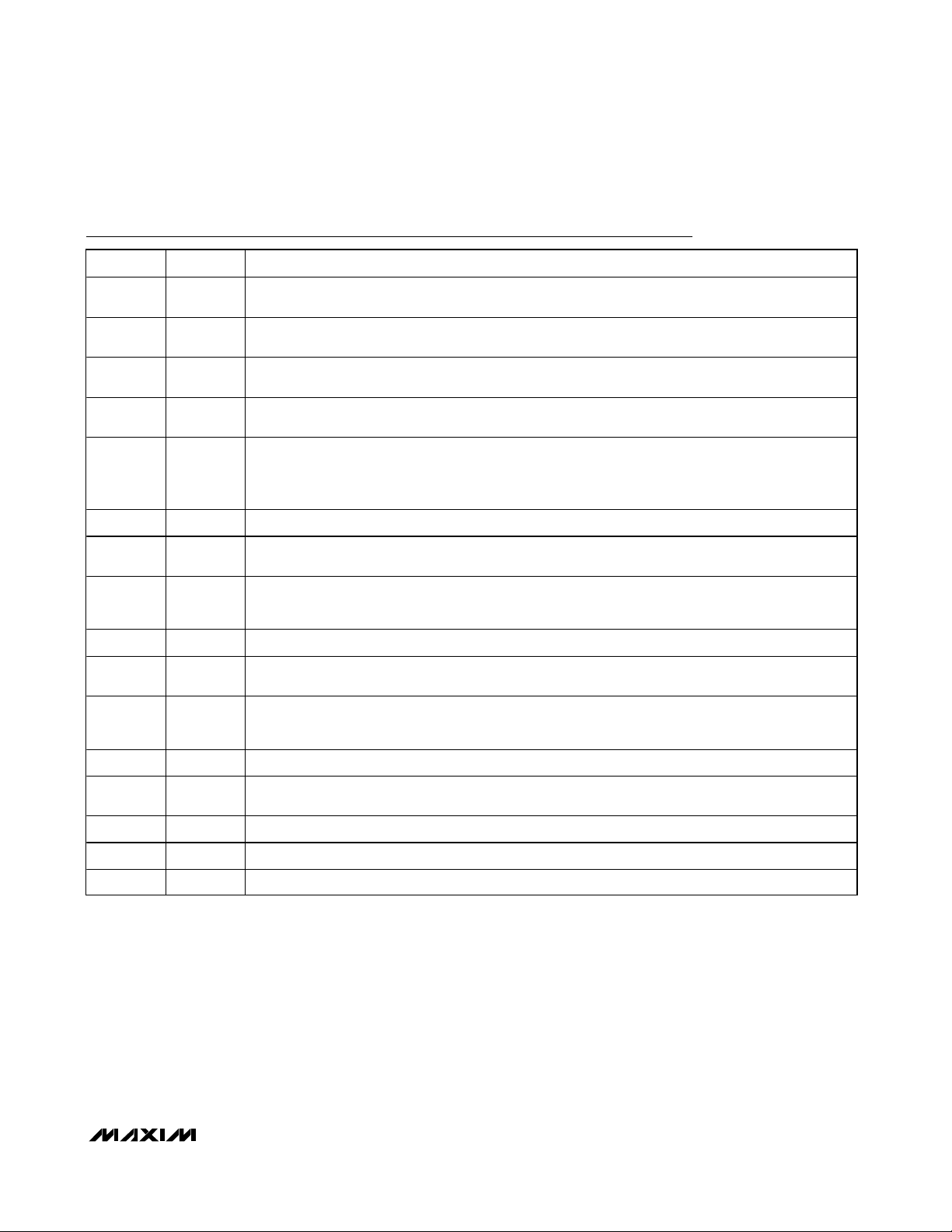
CORE LINE-TRANSIENT RESPONSE
(3.3V TO 5V)
100µs/div
MAX1775 toc10
MAIN LOAD TRANSIENT (IN DROPOUT
LOAD FROM 50mA TO 500mA)
200µs/div
MAX1775 toc12
5V
V
1V/div
3.3V
V
CORE
50mV/div
400mA
200mA
0
V
MAIN
50mV/div
MAIN LOAD TRANSIENT
(LOAD FROM 100mA to 1A, V
INC
200µs/div
IN
MAX1775 toc11
100mA
= 5V)
1A
I
MAIN
0
V
MAIN
50mV/div
TURN-ON RESPONSE
I
MAIN
(CIRCUIT OF FIGURE 4), NO LOAD
100µs/div
MAX1775 toc13
5V
0
3V
2V
1V
0
400mA
200mA
0mA
SHDNM
V
MAIN
V
CORE
I
IN
Page 9
MAX1775
Dual-Output Step-Down
DC-DC Converter for PDA/Palmtop Computers
_______________________________________________________________________________________ 9
Pin Description
PIN NAME FUNCTION
1 SHDNM
2 SHDNC
3 PGND
4 NDRV
5 CVL
6 IN Power Supply Input
7 PDRV
8 CVH
9 REF Reference Voltage Output. Bypass REF to GND with a 0.22µF or greater capacitor.
10 FBM
11 CS+
12 CS- Main Regulator Low-Side Current-Sense Input. Connect CS- to the main output.
13 FBC
14 GND Analog Ground
Shutdown for Main Regulator. A low voltage on SHDNM shuts off the main output. For normal
operation, connect SHDNM to IN.
Shutdown for Core Regulator. A low voltage on SHDNC shuts off the core output. For normal operation,
connect SHDNC to CVL.
Power Ground. Ground for NDRV and core output synchronous rectifier. Connect all grounds together
close to the IC.
N-Channel Drive Output. Drives the main output synchronous rectifier MOSFET. NDRV swings between
CVL and PGND.
Low-Side Regulator Bypass. CVL is the output of an internal LDO regulator. This is the internal power
supply for the device control circuitry as well as the N-channel driver. Bypass CVL with a 1.0µF or
greater capacitor to GND. When CS- is above the CVL switchover threshold (2.47V), CVL is powered
from the main output.
P-Channel Drive Output. Drives the main output high-side MOSFET switch. PDRV swings between IN
and CVH. The voltage at CVH is regulated at V
High-Side Drive Bypass. CVH is the output of an internal LDO regulator with respect to V
low-side of the P-channel driver output. Bypass with a 1.0µF capacitor or greater to IN. When the input
voltage is less than +5.5V, CVH is switched to PGND.
Main Output Feedback. Connect FBM to a resistive voltage-divider to set main output voltage between
+1.25V to +5.5V.
Main Regulator High-Side Current-Sense Input. Connect the sense resistor between CS+ and CS-.
This voltage is used to set the current limit and to turn off the synchronous rectifier when the inductor
current approaches zero.
Core Output Feedback. Connect FBC to a resistive voltage-divider to set core output between +1.0V to
+5.0V.
- 4.3V unless the input voltage is less than 5.5V.
IN
. This is the
IN
15 INC Core Supply Input
16 LXC Core Converter Switching Node
Page 10

MAX1775
Dual-Output Step-Down
DC-DC Converter for PDA/Palmtop Computers
10 ______________________________________________________________________________________
Detailed Description
The MAX1775 dual step-down DC-DC converter is
designed to power PDA, palmtop, and subnotebook
computers. Normally, these devices need two separate
power supplies—one for the processor and another
higher voltage supply for the peripheral circuitry. The
MAX1775 provides an adjustable +1.25V to +5.5V main
output designed to power the peripheral circuitry of
PDAs and similar devices. The main output delivers
over 2A output current. The lower voltage core converter has an adjustable +1.0V to +5.0V output, providing
up to 1.5A output current. Both regulators utilize a proprietary regulation scheme, allowing PWM operation at
medium to heavy loads, and automatically switch to
pulse skipping at light loads for improved efficiency.
Figure 1 is the typical application circuit.
Operating Modes for the
Step-Down Converters
When delivering low output currents, the MAX1775
operates in discontinuous conduction mode. Current
through the inductor starts at zero, rises above the minimum current limit, then ramps down to zero during
each cycle (see Typical Operating Characteristics).
The switch waveform may exhibit ringing, which occurs
at the resonant frequency of the inductor and stray
capacitance, due to the residual energy trapped in the
core when the rectifier MOSFET turns off. This does not
degrade the circuit performance.
When delivering medium-to-high output currents, the
MAX1775 operates in PWM continuous-conduction
mode. In this mode, current always flows through the
inductor and never ramps to zero. The control circuit
adjusts the switch duty cycle to maintain regulation
without exceeding the peak switching current set by
the current-sense resistor.
100% Duty Cycle and Dropout
The MAX1775 operates with a duty cycle up to 100%.
This feature extends the input voltage range by turning
the MOSFET on continuously when the supply voltage
approaches the output voltage. This services the load
when conventional switching regulators with less than
100% duty cycle would fail. Dropout voltage is defined
as the difference between the input and output voltages when the input is low enough for the output to
drop out of regulation. Dropout depends on the MOSFET drain-to-source on-resistance, current-sense resistor, and inductor series resistance, and is proportional
to the load current:
Dropout voltage =
I
OUT
✕
[R
DS(ON)
+ R
SENSE
+ R
INDUCTOR
]
Figure 1. Typical Application Circuit (Low Input Voltage)
IN
2.7V TO 5.5V
C1
1µF
8
6
IN
CVH
ON
ON
1µF
0.22µF
15
INC
PDRV
NDRV
CS+
CS-
FBM
LXC
FBC
M1
7
4
M2
11
12
10
L
C
5.4µH
16
13
1
OFF
SHDNM
2
SHDNC
OFF
5
C2
C3
CVL
MAX1775
9
REF
3
PGND
14
GND
R4
R5
L
5µH
C6
10µF
M
R1
33mΩ
C5
22µF
CORE
1.8V
1.5A
MAIN
3.3V
2A
C4
R2
47µF
R3
Page 11

MAX1775
Dual-Output Step-Down
DC-DC Converter for PDA/Palmtop Computers
______________________________________________________________________________________ 11
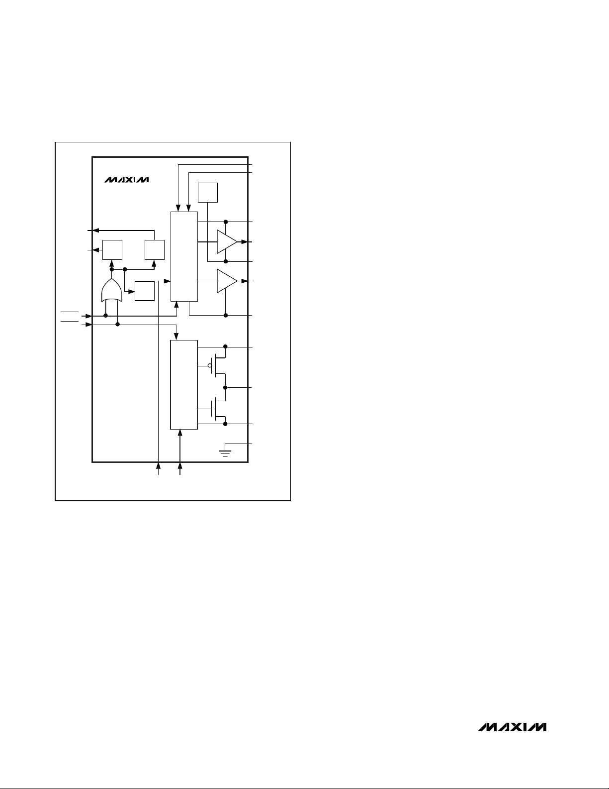
Regulation Control Scheme
The MAX1775 has a unique operating scheme that
allows PWM operation at medium and high current, with
automatic switching to pulse-skipping mode at lower
currents to improve light-load efficiency. Figure 2
shows a simplified block diagram.
Under medium- and heavy-load operation, the inductor
current is continuous and the part operates in PWM
mode. In this mode, the switching frequency is set by
either the minimum on-time or the minimum off-time,
depending on the duty cycle. The duty cycle is approximately the output voltage divided by the input voltage.
If the duty cycle is less than 50%, the minimum on-time
controls the frequency; and the frequency is approximately f ≈ 2.5MHz ✕D, where D is the duty cycle. If the
duty cycle is greater than 50%, the minimum off-time
sets the frequency; and the frequency is approximately
f ≈ 2.5MHz ✕(1 - D).
In both cases, the voltage is regulated by the error
comparator. For low duty cycles (<50%), the P-channel
MOSFET turns on for the minimum on-time, causing
fixed-on-time operation. During the P-channel MOSFET
on-time, the output voltage rises. Once the P-channel
MOSFET turns off, the voltage drops to the regulation
threshold, at which time another cycle is initiated. For
high duty cycles (>50%), the P-channel MOSFET
remains off for the minimum off-time, causing fixed offtime operation. In this case, the P-channel MOSFET
remains on until the output voltage rises to the regulation threshold. Then the P-channel MOSFET turns off for
the minimum off-time, initiating another cycle.
By switching between fixed on-time and fixed off-time
operation, the MAX1775 can operate at high input-output ratios, yet still operate up to 100% duty cycle for
low dropout. Note that when operating in fixed on-time,
the minimum output voltage is regulated; but in fixed
off-time operation, the maximum output voltage is regulated. Thus, as the input voltage drops below approximately twice the output voltage, a decrease in line
regulation can be expected. The drop in voltage is
approximately V
DROP
≈ V
RIPPLE
. At light output loads,
the inductor current is discontinuous, causing the
MAX1775 to operate at lower frequencies, reducing the
MOSFET gate drive and switching losses. In discontinuous mode, under most circumstances, the on-time will
be a fixed minimum of 400ns.
The MAX1775 features four separate current-limit
threshold detectors and a watchdog timer for each of
its step-down converters. In addition to the more common peak current detector and zero crossing detector,
each converter also provides a valley current detector
(I
VALLEY
) and a minimum current detector (I
MIN
). I
VALLEY
is used to force the inductor current to drop to a lower
level after hitting peak current before allowing the Pchannel MOSFET to turn on. This is a safeguard against
inductor current significantly overshooting above the
peak current when the inductor discharges too slowly
when V
OUT
/L is small. I
MIN
is useful in ensuring that a
minimum current is built up in the inductor before turning off the P-channel MOSFET. This helps the inductor
to charge the output near dropout when dI/dt is small
(because (V
IN
- V
OUT
) / L is small) to avoid multiple
Figure 2. Simplified Control System Block Diagram
TOFFMIN
V
MIN
CS+
CS-
V
VALLEY
FB
V
REF
TONMIN
R
PON
QS
PON
V
IN
PSW
V
O
V
CLM
V
ZERO
NON
Q
S
R
NONOVERLAP
PROTECTION
NSW
Page 12
MAX1775
Dual-Output Step-Down
DC-DC Converter for PDA/Palmtop Computers
12 ______________________________________________________________________________________
pulses and low efficiency. This feature, however, is disabled during dropout and light-load conditions where
the inductor current may take too long to reach the I
MIN
value. A watchdog timer overrides I
MIN
after the Pchannel MOSFET has been on for longer than about
10µs.
Main Step-Down Converter
The main step-down converter features adjustable
+1.25V to +5.5V output, delivering over 2A from a
+2.7V to +28V input (see Setting the Output Voltages).
The use of external MOSFETs and a current-sense
resistor maximizes design flexibility. The MAX1775
offers a synchronous rectifier MOSFET driver that
improves efficiency by eliminating losses through a
diode. The two MOSFET drive outputs, PDRV and
NDRV, control these external MOSFETs. The output
swing of these outputs is limited to reduce power con-
sumption by limiting the amount of injected gate charge
(see Internal Linear Regulators). The main current limit
is sensed through a small sense resistor at the converter output (see Setting the Current Limit). Driving SHDNM
low puts the main converter in a low-power shutdown
mode. The core regulator is still functional when the
main converter is in shutdown.
Core Step-Down Converter
The core step-down converter produces a +1.0V to
+5.0V output from a +2.6V to +5.5V input. The low-voltage input allows the use of internal power MOSFETs, taking advantage of their low R
DS(ON)
, improving efficiency
and reducing board space. Like the main converter, the
core regulator makes use of an N-channel MOSFET synchronous rectifier, improving efficiency and eliminating
the need for an external Schottky diode. Current sensing
is internal to the device, eliminating the need for an
external sense resistor. The maximum and minimum current limits are sensed through the P-channel MOSFET,
while the valley current and zero crossing current are
sensed through the N-channel MOSFET. The core output
voltage is measured at FBC through a resistive voltagedivider. This divider can be adjusted to set the output
voltage level (see Setting the Output Voltages). The core
input can be supplied from the main regulator or an
external supply that does not exceed +5.5V (see High-
Voltage Configuration and Low-Voltage Configuration).
The core converter can be shut down independent of the
main converter by driving SHDNC low. If the main converter output is supplying power to the core and is shut
down, SHDNM controls both outputs. Figure 3 is a simplified block diagram.
Internal Linear Regulators
There are two linear regulators internal to the MAX1775. A
high-voltage linear regulator accepts inputs up to +28V,
reducing it to +2.8V at CVL to provide power to the
MAX1775. Once the voltage at CS- reaches +2.47V, CVL
is switched to CS, allowing it to be driven from the main
converter, improving efficiency. CVL supplies the internal
bias to the IC and power for the NDRV gate driver.
The CVH regulator provides the low-side voltage for the
main regulator’s PDRV output. The voltage at CVH is regulated at 4.3V below VINto limit the voltage swing on
PDRV, reducing gate charge and improving efficiency
(Figure 3).
Reference
The MAX1775 has an accurate internally trimmed
+1.25V reference at REF. REF can source no more than
50µA. Bypass REF to GND with a 0.22µF capacitor.
Figure 3. Simplified Block Diagram
MAX1775
CVL
REF
SHDNM
SHDNC
REF
SOFT-
START
CVL
FBM FBC
CS-
FB
ON
ON
MAIN
BUCK
CORE
BUCK
FB
CS+
CVH
CSCS+
IN
PDRV
CVH
NDRV
PGND
INC
LXC
PGNDC
GND
MAIN
OUT
Page 13
MAX1775
Dual-Output Step-Down
DC-DC Converter for PDA/Palmtop Computers
______________________________________________________________________________________ 13
Design Procedure
Low-Voltage Configuration
To improve efficiency and conserve board space, the
core regulator operates from low input voltages, taking
advantage of internal low-voltage, low-on-resistance
MOSFETs. When the input voltage remains below 5.5V,
run the core converter directly from the input by connecting INC to IN (Figure 1). This configuration takes
advantage of the core’s low-voltage design and
improves efficiency.
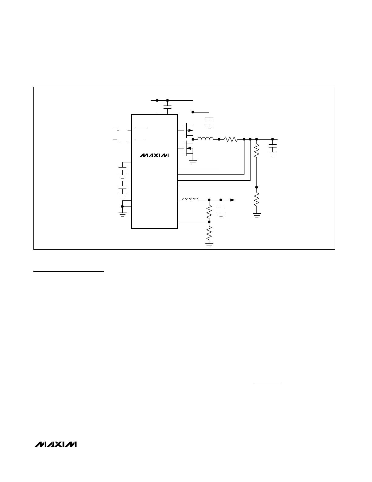
High-Voltage Configuration
For input voltages greater than 5.5V, cascade the main
and core converters by connecting INC to the main output voltage. In this configuration (Figure 4), the core
converter is powered from the main output. Ensure that
the main output can simultaneously supply its load and
the core input current. In this configuration, the main
output voltage must be set above the 2.6V minimum
input voltage of the core converter.
Setting the Output Voltages
The main output voltage may be set from +2.6V and
+5.5V with two external resistors connected as a volt-
age-divider to FBM (Figure 1). Resistor values can be
calculated by the following equation:
R2 = R3 ✕[(V
OUTM
/ V
FBM
) - 1]
where V
FBM
= +1.25V. Choose R3 to be 40kΩ or less.
The core regulator output is adjustable from +1.0V to
+5.0V through two external resistors connected as a
voltage-divider to FBC (Figure 1). Resistor values can
be calculated through the following equation:
R4 = R5
✕
[(V
OUTC
/ V
FBC
) - 1]
where V
FBC
= +1.0V. Choose R5 to be 30kΩ or less.
Setting the Current Limit
The main regulator current limit is set externally through
a small current-sense resistor, R1 (Figure 1). The value
of R1 can be calculated by the following equation:
where V
CLM
= 80mV is the current-sense threshold,
and I
OUT
is the current delivered to the output. The
core converter current limit is set internally and cannot
be modified.
()
Figure 4. High Input Voltage Cascaded Configuration
IN 2.7V TO 28V
ON
ON
0.22µF
1µF
1
OFF
SHDNM
2
SHDNC
OFF
5
CVL
C2
C3
MAX1775
9
REF
3
PGND
14
GND
C1
6
1µF
8
IN
CVH
PDRV
NDRV
CS+
CS-
INC
FBM
LXC
FBC
M1
7
4
M2
11
12
15
10
L
C
5.4µH
16
13
10µH
R4
R5
C6
10µF
R1
33mΩ
L
M
CORE
1.8V
C5
1.5A
22µF
MAIN
3.3V
2A
R2
R3
C4
47µF
R
113 =
V
.
CLM
I
OUT
Page 14

MAX1775
Dual-Output Step-Down
DC-DC Converter for PDA/Palmtop Computers
14 ______________________________________________________________________________________
Careful layout of the current-sense signal traces is
imperative. Place R1 as close to the MAX1775 as possible. The two traces should have matching length and
width, be as far as possible from noisy switching signals, and be close together to improve noise rejection.
These traces should be used for current-sense signal
routing only and should not carry any load current.
Refer to the MAX1775 Evaluation Kit for layout examples.
Inductor Selection
The essential parameters for inductor selection are
inductance and current rating. The MAX1775 operates
with a wide range of inductance values.
Calculate the inductance value for either core or main,
L
MIN
:
L
MIN
= (VIN- V
OUT
) ✕T
ONMIN
/ I
RIPPLE
where T
ONMIN
is typically 400ns, and I
RIPPLE
is the
continuous conduction ripple current. In continuous
conduction, I
RIPPLE
should be chosen to be 30% of the
maximum load current. With high inductor values, the
MAX1775 begins continuous-conduction operation at a
lower fraction of full load (see Detailed Description).
The inductor’s saturation current must be greater than
the peak switching current to prevent core saturation.
Saturation occurs when the inductor’s magnetic flux
density reaches the maximum level the core can support, and inductance starts to fall. The inductor heating
current rating must be greater than the maximum load
current to prevent overheating. For optimum efficiency,
the inductor series resistance should be less than the
current-sense resistance.
Capacitor Selection
Choose output filter capacitors to service the output ripple current with acceptable voltage ripple. ESR in the
output capacitor is a major contributor to output ripple.
For the main converter, low-ESR capacitors such as
polymer, ceramic, or even tantalum are recommended.
For the core converter, choosing a low-ESR tantalum
capacitor with enough ESR to generate about 1% ripple
voltage across the output is helpful in ensuring stability.
Voltage ripple is the sum of contributions from ESR and
the capacitor value:
V
RIPPLE
≈ V
RIPPLE,ESR
+ V
RIPPLE,C
For tantalum capacitors, the ripple is determined mostly
by the ESR. Voltage ripple due to ESR is:
V
RIPPLE,ESR
≈ R
ESR
✕
I
RIPPLE
For ceramic capacitors, the ripple is mostly due to the
capacitance. The ripple due to the capacitance is
approximately:
V
RIPPLE
,C
≈ L I
RIPPLE
2
/ 2C
OUTVOUT
where V
OUT
is the average output voltage. From this
equation, estimate the output capacitor values for given
voltage ripple as follows:
C
OUT
=
1/2
✕
L I
RIPPLE
2
/ (V
RIPPLE,COUT
✕
V
OUT)
This equation is suitable for initial capacitor selection.
Final values should be set by testing a prototype or evaluation kit. When using tantalum capacitors, use good soldering practices to prevent excessive heat from
damaging the devices and increasing their ESR. Also,
ensure that the tantalum capacitors’ surge-current ratings
exceed the startup inrush and peak switching currents.
The input filter capacitor reduces peak currents drawn
from the power source and reduces noise and voltage
ripple at IN, caused by the circuit’s switching. Use a
low-ESR capacitor. Two smaller-value low-ESR capacitors can be connected in parallel if necessary. Choose
input capacitors with working voltage ratings higher
than the maximum input voltage. Typically 4µF of input
capacitance for every 1A of load current is sufficient.
More capacitance may improve battery life and noise
immunity.
Place a surface-mount ceramic capacitor at IN very close
to the source of the high-side P-channel MOSFET. This
capacitor bypasses the MAX1775, minimizing the effects
of spikes and ringing on the MAX1775’s operation.
Bypass REF with 0.22µF or greater. Place this capacitor
within 0.2in (5mm) of the IC, next to REF, with a direct
trace to GND.
MOSFET Selection
The MAX1775 drives an external enhancement-mode
P-channel MOSFET and a synchronous-rectifier Nchannel MOSFET. When selecting the MOSFETs,
important parameters to consider are on-resistance
(R
DS(ON)
), maximum drain-to-source voltage
(V
DS(MAX)
), maximum gate-to-source voltage
(V
GS(MAX)
), and minimum threshold voltage (V
TH(MIN)
).
Chip Information
TRANSISTOR COUNT: 3530
PROCESS: BiCMOS
Page 15

Dual-Output Step-Down
DC-DC Converter for PDA/Palmtop Computers
Maxim cannot assume responsibility for use of any circuitry other than circuitry entirely embodied in a Maxim product. No circuit patent licenses are
implied. Maxim reserves the right to change the circuitry and specifications without notice at any time.
Maxim Integrated Products, 120 San Gabriel Drive, Sunnyvale, CA 94086 408-737-7600 ____________________ 15
© 2001 Maxim Integrated Products Printed USA is a registered trademark of Maxim Integrated Products.
Package Information
MAX1775
QSOP.EPS
 Loading...