

Page 1
General Description
The MAX1765 is a high-efficiency, low-noise, step-up
DC-DC converter intended for use in battery-powered
wireless applications. This device operates at a high
1MHz fixed frequency while maintaining an exceptionally low quiescent supply current (200µA). Its small
external components and tiny package make this
device an excellent choice for small hand-held applications that require the longest possible battery life.
The MAX1765 uses a synchronous-rectified pulsewidth-modulation (PWM) boost topology to generate
2.5V to 5.5V outputs from a wide range of input
sources, such as one to three alkaline or NiCd/NiMH
cells or a single lithium-ion (Li+) cell. Maxim's proprietary architecture significantly improves efficiency at
low load currents while automatically transitioning to
fixed-frequency PWM operation at medium to high load
currents to maintain excellent full-load efficiency.
Forced-PWM mode is available for applications that
require constant-frequency operation at all load currents, and the MAX1765 may also be synchronized to
an external clock to protect sensitive frequency bands
in communications equipment.
The MAX1765’s low-dropout (LDO) linear regulator and
DC-DC converter have separate shutdown control. The
linear regulator's 250mΩ pass device maintains excellent dropout voltage at currents up to 500mA. The
MAX1765 also features analog soft-start and currentlimit functions to permit optimization of efficiency, external component size, and output voltage ripple.
The MAX1765 comes in a 16-pin QSOP package and a
thermally enhanced 16-pin TSSOP-EP.
____________________________Features
♦ High-Efficiency Step-Up Converter
Up to 93% Efficiency
Adjustable Output from +2.5V to +5.5V
Up to 800mA Output
PWM Synchronous-Rectified Topology
1MHz Operating Frequency (or Sync)
♦ LDO Linear Regulator
500mA LDO Linear Regulator
2.85V Linear Regulator Output or Adjustable
(1.25V to 5V)
Low 125mV Dropout at 500mA
♦ +0.7V to +5.5V Input Range
♦ 0.1µA Logic-Controlled Shutdown
♦ Adjustable Inductor Current Limit and Soft-Start
♦ Thermal Shutdown
♦ 1.5W, 16-Pin TSSOP-EP Package Available
MAX1765
800mA, Low-Noise, Step-Up DC-DC Converter
with 500mA Linear Regulator
________________________________________________________________ Maxim Integrated Products 1
19-1805; Rev 0; 12/00
For price, delivery, and to place orders, please contact Maxim Distribution at 1-888-629-4642,
or visit Maxim’s website at www.maxim-ic.com.
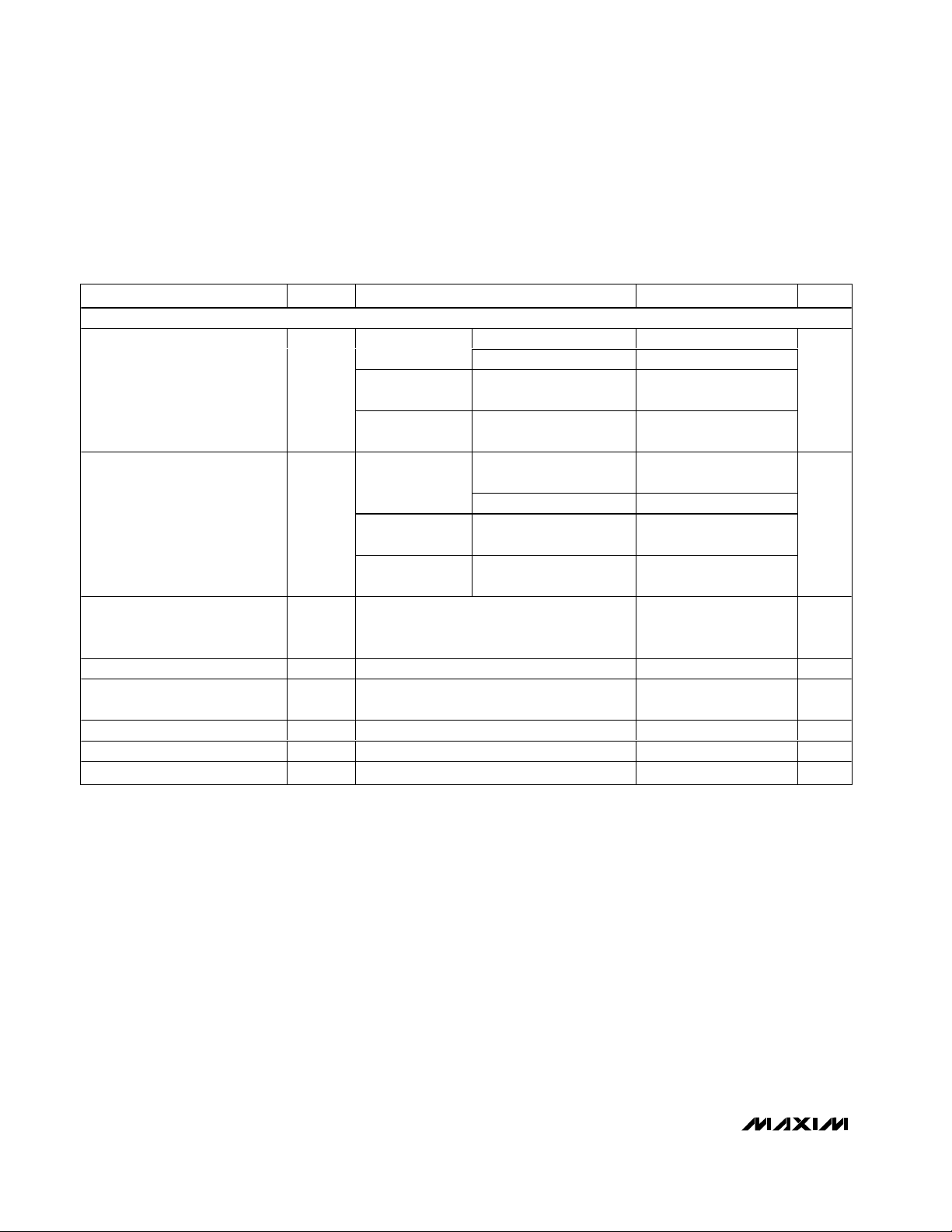
16
15
14
13
12
11
10
9
1
2
3
4
5
6
7
8
FBL ONL
TRACK
INL
POUT
LX
PGND
OUTL
TOP VIEW
MAX1765
QSOP/TSSOP-EP
ONB
ISET
REF
OUT
GND
FB
ONA
CLK/SEL
Pin Configuration
Wireless Handsets
PCS Phones
Palmtop Computers
Personal
Communicators
Hand-Held Instruments
Portable Audio Players
Applications
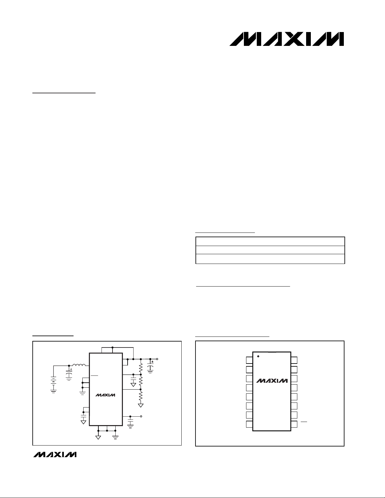
Typical Operating Circuit
Ordering Information
*Exposed pad
PART
PIN-PACKAGE
MAX1765EEE
16 QSOP
MAX1765EUE
16 TSSOP-EP*
TEMP. RANGE
-40°C to +85°C
-40°C to +85°C
(0.7V TO 5.5V)
3.3µH
ONL
LX
ONB
CLK/SEL
TRACK
MAX1765
REF
ILIM
GND PGND
FBL
ONA
POUT
INL
OUT
OUTL
OUT = 3.3V
FB
OUTL = 2.85V
(ADJ 1.25V
TO 5V)
Page 2
MAX1765
800mA, Low-Noise, Step-Up DC-DC Converter
with 500mA Linear Regulator
2 _______________________________________________________________________________________
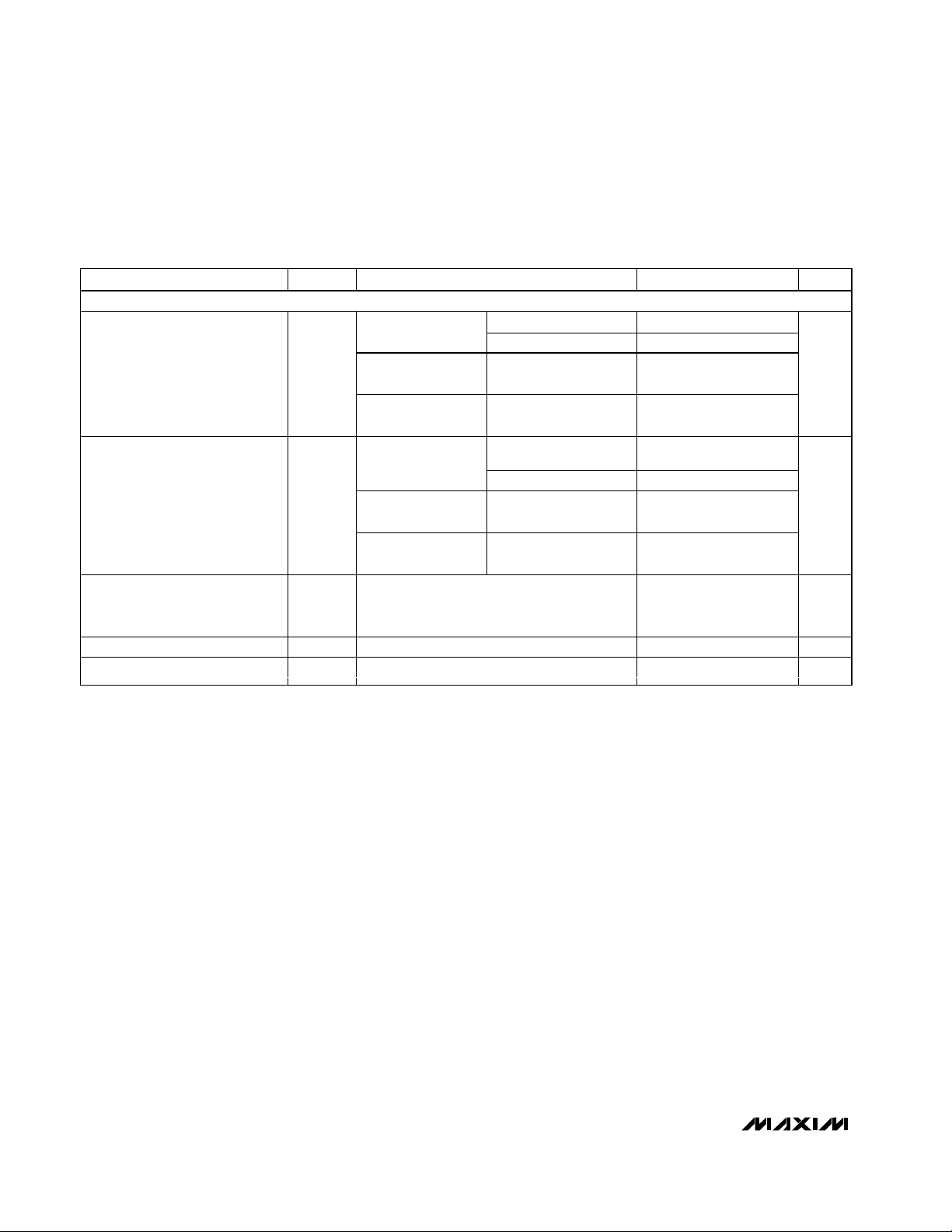
ABSOLUTE MAXIMUM RATINGS
ELECTRICAL CHARACTERISTICS
(V
OUT
= V
POUT
= V
INL
= V
ONA
= V
ONL
= 3.6V, CLK/SEL = FBL = ONB = TRACK = PGND = GND, ISET = REF (bypassed with
0.22µF), LX = open, OUTL = open (bypassed with 4.7µF), T
A
= 0°C to +85°C, unless otherwise noted. Typical values are at
T
A
= +25°C.)
Stresses beyond those listed under “Absolute Maximum Ratings” may cause permanent damage to the device. These are stress ratings only, and functional
operation of the device at these or any other conditions beyond those indicated in the operational sections of the specifications is not implied. Exposure to
absolute maximum rating conditions for extended periods may affect device reliability.
ONA, ONB, ONL, TRACK, OUT, INL to GND..............-0.3V, +6V
PGND to GND.....................................................................±0.3V
LX to GND ...............................................-0.3V to (POUT + 0.3V)
OUTL to GND ..............................................-0.3V to (INL + 0.3V)
CLK/SEL, REF, FB, FBL, ISET, POUT
to GND...................................................-0.3V to (OUT + 0.3V)
OUTL Short Circuit .....................................................Continuous
Continuous Power Dissipation (T
A
= +70°C)
16-Pin QSOP (derate 8.3mW/°C above +70°C)...........667mW
16-Pin TSSOP-EP (derate 19mW/°C above +70°C) ....1500mW
Operating Temperature Range ...........................-40°C to +85°C
Junction Temperature......................................................+150°C
Storage Temperature Range .............................-65°C to +150°C
Lead Temperature (soldering, 10s) .................................+300°C
V
OUTL
+ 0.4
V
OUTL
+ 0.5
V
OUTL
+ 0.6
DC-DC CONVERTER
Input Voltage Range (Note 1) 0.7 5.5 V
INL Voltage Range (Note 1) 2.3 5.5 V
Minimum Startup Voltage I
Temperature Coefficient of
Startup Voltage
FB Regulation Voltage V
FB Input Leakage Current VFB = 1.35V 0.01 100 nA
Output Voltage Adjust Range 2.5 5.5 V
Load Regulation CLK/SEL = OUT, 0 < I
OUT Voltage in Track Mode V
Frequency in Startup Mode f
Startup to Normal Mode
Transition Voltage
ISET Input Leakage Current V
Supply Current in Normal Mode
(Note 3)
Supply Current in Low-Noise
PWM Mode (Note 3)
Supply Current in Shutdown ONA = ONL = GND, ONB = OUT 1 10 µA
PARAMETER SYMBOL CONDITIONS MIN TYP MAX UNITS
LX
FB
< 1mA, T
LOAD
< 1mA -2 m V /°C
I
LOAD
CLK/SEL = OUT, 0 < ILX < 0.55A 1.215 1.250 1.275 V
> 2.0V, INL = POUT
OUTL
V
= 1.5V 125 1000 kHz
OUT
Rising edge only (Note 2) 2.00 2.15 2.30 V
= 1.25V 0.01 50 nA
ISET
CLK/SEL = ONL = GND, no load 100 200 µA
C LK/S E L = OU T,
no l oad
= +25°C, Figure 2 0.9 1.1 V
A
< 800mA -1 %
LOAD
VFB = 1.5V 130 200 µA
FB = GN D ( LX sw i tchi ng ) 2.5 mA
V
Page 3
MAX1765
800mA, Low-Noise, Step-Up DC-DC Converter
with 500mA Linear Regulator
_______________________________________________________________________________________ 3
ELECTRICAL CHARACTERISTICS (continued)
(V
OUT
= V
POUT
= V
INL
= V
ONA
= V
ONL
= 3.6V, CLK/SEL = FBL = ONB = TRACK = PGND = GND, ISET = REF (bypassed with
0.22µF), LX = open, OUTL = open (bypassed with 4.7µF), T
A
= 0°C to +85°C, unless otherwise noted. Typical values are at
T
A
= +25°C.)
DC-DC SWITCHES
POUT Leakage Current VLX = 0, V
LX Leakage Current V
Switch On-Resistance
N - C hannel C ur r ent Li m i t ( N ote 4) I
P-Channel Turn-Off Current CLK/SEL = GND 10 50 120 mA
REFERENCE
Reference Output Voltage V
Reference Load Regulation -1µA < I
Reference Supply Regulation 2.5V < V
LINEAR REGULATOR
INL Voltage Range (Note 1) 2.3 5.5 V
INL Startup Voltage V
Output Voltage in Internal
Feedback Mode
FBL Dual-Mode Threshold 150 250 350 mV
FBL Regulation Voltage V
FBL Input Leakage Current V
OUTL Adjust Range 1.25 5 V
Short-Circuit Current Limit V
Dropout Resistance V
Load Regulation 1mA < I
Line Regulation
INL Supply Current in Shutdown OUTL = ONA = ONL = GND 0.1 10 µA
INL No-Load Supply Current I
AC Power-Supply Rejection f = 10kHz 65 dB
Thermal Shutdown Hysteresis approximately 10°C 160 °C
PARAMETER SYMBOL CONDITIONS MIN TYP MAX UNITS
= 5.5V 0.1 10 µA
OUT
= V
LX
= V
OUT
= 5.5V, ONA = GND 0.1 10 µA
ONB
N-channel 0.17 0.28
P-channel 0.22 0.5
V
LIM
REF
INL
FBL
= 1.25V, CLK/SEL = GND or OUT 1000 1250 1600 mA
ISET
I
= 0 1.230 1.250 1.270 V
REF
< 50µA515mV
REF
< 5.5V 0.2 5 mV
OUT
V
= 2V, rising edge only 2.15 2.30 2.45 V
OUT
FBL = GND, I
FBL = OUTL, I
= 1.5V 0.01 50 nA
FBL
= 1V 550 1300 mA
FBL
= 1V, I
FBL
OUTL
2.5V < (V
OUT
FBL = OUTL
= 0, V
OUTL
= 10mA 2.80 2.85 2.90 V
OUTL
= 10mA, I
OUTL
= 500mA 0.25 0.5 Ω
OUTL
= 0 1.230 1.250 1.270 V
REF
< 500mA, FBL = GND 0.5 1 %
= V
= V
INL
= 5.5V 90 250 µA
INL
POUT
) < 5.5V,
-0.5 0.5 %
Ω
Page 4
MAX1765
800mA, Low-Noise, Step-Up DC-DC Converter
with 500mA Linear Regulator
4 _______________________________________________________________________________________
ELECTRICAL CHARACTERISTICS (continued)
(V
OUT
= V
POUT
= V
INL
= V
ONA
= V
ONL
= 3.6V, CLK/SEL = FBL = ONB = TRACK = PGND = GND, ISET = REF (bypassed with
0.22µF), LX = open, OUTL = open (bypassed with 4.7µF), T
A
= 0°C to +85°C, unless otherwise noted. Typical values are at
TA=+25 °C.)
CONTROL INPUTS
Input Low Level
Input High Level
Input Leakage Current
(CLK/SEL, ONA, ONB,
ONL, TRACK)
Internal Oscillator Frequency CLK/SEL = OUT 0.8 1 1.2 MHz
External Oscillator
Synchronization Range
Oscillator Maximum Duty Cycle 80 86 90 %
Minimum CLK/SEL Pulse 200 ns
M axi m um C LK/S E L Ri se/Fal l Ti m e 100 ns
PARAMETER SYMBOL CONDITIONS MIN TYP MAX UNITS
O N A, O NB, O N L
( N ote 5)
CLK/SEL 1.2V < V
TRACK 1.2V < V
O N A, O NB, O N L
( N ote 5)
CLK/SEL 1.2V < V
TRACK 1.2V < V
1.1V < V
1.8V < V
1.1V < V
1.8V < V
< 1.8V 0.2
OUT
< 5.5V 0.4
OUT
< 5.5V
OUT
< 5.5V
INL
V
< 1.8V
OUT
< 5.5V 1.6
OUT
< 5.5V
OUT
< 5.5V
INL
OUT
- 0.2
0.8 ×
V
OUT
0.8 ×
V
INL
0.01 1 µA
0.5 1.2 MHz
0.2 ×
V
OUT
0.2 ×
V
V
INL
V
Page 5

MAX1765
800mA, Low-Noise, Step-Up DC-DC Converter
with 500mA Linear Regulator
_______________________________________________________________________________________ 5
ELECTRICAL CHARACTERISTICS
(V
OUT
= V
POUT
= V
INL
= V
ONA
= V
ONL
= 3.6V, CLK/SEL = FBL = ONB = TRACK = PGND = GND, ISET = REF (bypassed with
0.22µF), LX = open, OUTL = open (bypassed with 4.7µF), T
A
= -40°C to +85°C, unless otherwise noted.) (Note 6)
PARAMETER
CONDITIONS
UNITS
DC-DC CONVERTER
FB Regulation Voltage V
FB
CLK/SEL = OUT, 0 < ILX < 0.55A
V
OUT Voltage in Track Mode V
OUTL
> 2.0V, INL = POUT
V
OUTL
V
OUTL
V
Startup to Normal Mode
Transition Voltage
Rising edge only (Note 2)
V
Supply Current in Normal Mode
(Note 3)
CLK/SEL = ONL = GND, no load
µA
Supply Current in
Low-Noise PWM Mode (Note 3
C LK/S E L = OU T, V
FB
= 1.5V , no l oad
µA
Supply Current in Shutdown ONA = ONL = GND, ONB = OUT 10 µA
DC-DC SWITCHES
POUT Leakage Current VLX = 0, V
OUT
= 5.5V 10 µA
LX Leakage Current V
LX
= V
OUT
= V
ONB
= 5.5V, ONA = GND 10 µA
N-channel
Switch On-Resistance
P-channel
Ω
N - C hannel C ur r ent Li m i t ( N ote 4)
I
LIM
V
ISET
= 1.25V, CLK/SEL = GND or OUT
mA
P-Channel Turn-Off Current CLK/SEL = GND 5
mA
REFERENCE
Reference Output Voltage I
REF
= 0
V
LINEAR REGULATOR
Output Voltage in Internal
Feedback Mode
FBL = GND, I
OUTL
= 10mA
V
FBL Input Threshold
mV
FBL Regulation Voltage FBL = OUTL, I
OUTL
= 10mA, I
REF
= 0
V
LDO Startup Voltage V
OUT
= 2V, rising edge only
V
Dropout Resistance V
FBL
= 1V, I
OUTL
= 500mA 0.5 Ω
INL Supply Current in Shutdown
OUTL = ONA = ONL = GND 10 µA
INL No-Load Supply Current I
OUTL
= 0, V
INL
= 5.5V
µA
SYMBOL
MIN TYP MAX
1.210 1.280
+ 0.4
+ 0.6
2.00 2.30
200
200
0.28
0.50
1000 1600
1.225 1.275
120
2.79 2.90
150 350
1.225 1.275
2.15 2.45
250
Page 6
MAX1765
800mA, Low-Noise, Step-Up DC-DC Converter
with 500mA Linear Regulator
6 _______________________________________________________________________________________
ELECTRICAL CHARACTERISTICS (continued)
(V
OUT
= V
POUT
= V
INL
= V
ONA
= V
ONL
= 3.6V, CLK/SEL = FBL = ONB = TRACK = PGND = GND, ISET = REF (bypassed with
0.22µF), LX = open, OUTL = open (bypassed with 4.7µF), T
A
= -40°C to +85°C, unless otherwise noted.) (Note 6)
Note 1: Operating voltage. Since the regulator is bootstrapped to the output, once started it will operate down to 0.7V input.
Note 2: The device is in startup mode when V
OUT
is below this value (see Low-Voltage Startup Oscillator section). Do not apply full
load current.
Note 3: Supply current into the OUT and POUT pins. This current correlates directly to the actual battery-supply current, but is
reduced in value according to the step-up ratio and efficiency.
Note 4: Minimum recommended ISET voltage in normal mode is 0.625V.
Note 5: ONA, ONB, ONL have hysteresis of approximately 0.15
✕
V
OUT
.
Note 6: Specifications to -40°C are guaranteed by design and not production tested.
CONTROL INPUTS
Input Low Level
Input High Level
Input Leakage Current
(CLK/SEL, ONA, ONB,
ONL, TRACK)
Internal Oscillator Frequency CLK/SEL = OUT 0.8 1.2 MHz
Oscillator Maximum Duty Cycle 79 90 %
PARAMETER SYMBOL CONDITIONS MIN TYP MAX UNITS
O N A, O NB, O N L
( N ote 5)
CLK/SEL 1.2V < V
TRACK 1.2V < V
O N A, O NB, O N L
( N ote 5)
CLK/SEL 1.2V < V
TRACK 1.2V < V
1.1V < V
1.8V < V
1.1V < V
1.8V < V
< 1.8V 0.2
OUT
< 5.5V 0.4
OUT
< 5.5V
OUT
< 5.5V
INL
V
< 1.8V
OUT
< 5.5V 1.6
OUT
< 5.5V
OUT
< 5.5V
INL
OUT
- 0.2
0.8 ×
V
OUT
0.8 ×
V
INL
0.2 ×
V
0.2 ×
V
OUT
INL
1 µA
V
V
Page 7

MAX1765
800mA, Low-Noise, Step-Up DC-DC Converter
with 500mA Linear Regulator
_______________________________________________________________________________________ 7
Typical Operating Characteristics
(TA = +25°C, unless otherwise noted.)
0
0.001 10.10.01
TRACK MODE EFFICIENCY vs. LOAD CURRENT
(V
OUTL
= +5V)
30
10
70
50
90
40
20
80
60
MAX1765 toc05
LOAD CURRENT (A)
EFFICIENCY (%)
VIN = +1.2V
VIN = +1.2V
VIN = +3.6V
NORMAL MODE
VIN = +2.4V
VIN = +3.6V
VIN = +2.4V
PWM
MODE
0
0.05
0.10
0.15
0.20
0.25
0.30
0 200100 300 400 500 600 700 800
LINEAR REGULATOR DROPOUT
VOLTAGE vs. LOAD CURRENT
MAX1765 toc07
LOAD CURRENT (mA)
DROPOUT VOLTAGE (V)
V
OUTL
= +2.5V
V
OUTL
= +2.85V
V
OUTL
= +5V
0
1 100010010
STARTUP INPUT VOLTAGE
vs. OUTPUT CURRENT
2.5
1.0
0.5
2.0
1.5
MAX1765 toc08
OUTPUT CURRENT (mA)
STARTUP INPUT VOLTAGE (V)
TA = +25°C
TA = -40°C
TA = +85°C
0
4
2
10
8
6
16
14
12
18
0 1.0 1.50.5 2.0 2.5 3.0 3.5
NO-LOAD SUPPLY CURRENT
vs. INPUT VOLTAGE
MAX1765 toc09
INPUT VOLTAGE (V)
SUPPLY CURRENT (mA)
FPWM MODE
NORMAL MODE
0.9
0
0.001 10.10.01
EFFICIENCY vs. LOAD CURRENT
(V
OUT
= +3.3V)
0.3
0.1
0.7
0.5
1.0
0.4
0.2
0.8
0.6
MAX1765 toc01
LOAD CURRENT (A)
EFFICIENCY (%)
VIN = +2.4V
NORMAL
MODE
VIN = +1.2V
VIN = +2.4V
VIN = +1.2V
PWM
MODE
90
0
0.001 10.10.01
EFFICIENCY vs. LOAD CURRENT
(V
OUT
= +5V)
30
10
70
50
100
40
20
80
60
MAX1765 toc02
LOAD CURRENT (A)
EFFICIENCY (%)
PWM
MODE
VIN = +1.2V
VIN = +2.4V
VIN = +3.6V
VIN = +3.6V
NORMAL MODE
VIN = +2.4V
VIN = +1.2V
90
0
0.001 10.10.01
TRACK MODE EFFICIENCY vs. LOAD CURRENT
(V
OUTL
= +2.85V)
30
10
70
50
100
40
20
80
60
MAX1765 toc03
LOAD CURRENT (A)
EFFICIENCY (%)
NORMAL MODE
V
IN
= +1.2V
VIN = +2.4V
VIN = +1.2V
VIN = +2.4V
PWM
MODE
0
0.001 10.10.01
TRACK MODE EFFICIENCY vs. LOAD CURRENT
(V
OUTL
= +3.3V)
30
10
70
50
90
40
20
80
60
MAX1765 toc04
LOAD CURRENT (A)
EFFICIENCY (%)
VIN = +1.2V
VIN = +1.2V
VIN = +2.4V
VIN = +3.6V
VIN = +2.4V
NORMAL
MODE
NORMAL MODE/
PWM MODE
PWM
MODE
0
600
400
200
800
1000
1200
0 2.01.50.5 1.0 2.5 3.0 3.5 4.0 4.5 5.0
MAXIMUM OUTPUT CURRENT
vs. INPUT VOLTAGE
MAX1765 toc06
INPUT VOLTAGE (V)
OUTPUT CURRENT (mA)
V
OUT
= +5V, I
SET
= REF
V
OUT
= +3.3V, I
SET
= REF
V
OUT
= +3.3V, I
SET
= 0.5 REF
V
OUT
= +5V, I
SET
= 0.5 REF
Page 8

MAX1765
800mA, Low-Noise, Step-Up DC-DC Converter
with 500mA Linear Regulator
8 _______________________________________________________________________________________
Typical Operating Characteristics (continued)
(TA = +25°C, unless otherwise noted.)
0
-10
-20
-30
-40
-50
-60
-70
-80
0.1 10 1001 1000
LDO PSRR vs. FREQUENCY
(100Hz TO 1MHz)
MAX1765 toc10
FREQUENCY (kHz)
LDO PSRR (dB)
16
0.1 1 10
BOOST FOLLOWED BY LDO
OUTPUT NOISE SPECTRUM
0
MAX1765 toc11
FREQUENCY (MHz)
NOISE (mV
RMS
)
4
2
8
10
6
12
14
VIN = +2.4V
V
OUT
= +3.3V
LINE TRANSIENT RESPONSE
(DC-DC)
MAX1765 toc12
100µs/div
A: VIN, 500mV/div
B: V
OUT
, 1mV/div, AC-COUPLED
A
B
V
OUT
= +3.3V, I = 0mA
V
IN
= +1.4V TO +2.4V
LINE TRANSIENT RESPONSE
(LINEAR)
MAX1765 toc13
A: VIN, 2V/div
B: V
OUT
, 5mV/div, AC-COUPLED
A
B
I = 0mA, V
IN
= +3V TO +5V, V
OUT
= +3.3V
TURN-ON WAVEFORMS
NO SOFT-START COMPONENTS
MAX1765 toc15a
A: 0NA, 5V/div
B: V
OUT
, 2V/div
C: INPUT CURRENT, 1A/div
A
B
C
SOFT-START WAVEFORMS
(R
SS
= 500kΩ, CSS = 0.1µF)
MAX1765 toc15b
A: 0NA, 5V/div
B: INPUT CURRENT, 100mA/div
C: V
OUT
, 1V/div
A
B
C
2.5ms/div
HEAVY-LOAD SWITCHING WAVEFORMS
(I
OUT
= 650mA, VIN = +2.4V, V
OUT
= 3.3V)
MAX1765 toc16
A: LX, 5V/div
B: INDUCTOR CURRENT, 200mA/div
C: OUTPUT RIPPLE, 50mV/div, AC-COUPLED
A
B
C
500ns/div
LOAD TRANSIENT RESPONSE
A
B
= +2.4V, V
V
IN
A: I
OUT
B: V
OUT
OUT
, 500mA/div
,100mV/div
= +3.3V, I
50µs/div
= 0 TO 500mA
OUT
MAX1765 toc14
Page 9

MAX1765
800mA, Low-Noise, Step-Up DC-DC Converter
with 500mA Linear Regulator
_______________________________________________________________________________________ 9
Pin Description
0
0.4
0.2
0.8
0.6
1.2
1.0
1.4
0 0.4 0.60.2 0.8 1.0 1.2 1.4
SWITCH CURRENT LIMIT vs. V
ISET
MAX1765 toc19
V
ISET
(V)
SWITCH CURRENT LIMIT (A)
V
OUT
= +3.3
Typical Operating Characteristics (continued)
(TA = +25°C, unless otherwise noted.)
LIGHT-LOAD SWITCHING WAVEFORMS
(V
IN
= +2.4V, V
OUT
= +3.3V, I
OUT
= 10mA)
MAX1765 toc17
A: LX NODE, 5V/div
B: INDUCTOR CURRENT, 200mA/div, AC-COUPLED
C: OUTPUT RIPPLE, 20mV/div, AC-COUPLED
A
B
C
500ns/div
450
0.1 1 10
LINEAR-REGULATOR OUTPUT NOISE
50
0
MAX1765 toc18
FREQUENCY (MHz)
NOISE (mV
RMS
)
150
250
350
I
LDO
= 200mA
V
LDO
= 2.85V
PIN NAME FUNCTION
1 FBL
2 ISET
3 REF
4 GND Ground. Connect to PGND with short trace.
5FB
6 OUT
7 ONA ON Input. When high, the DC-DC is operational (Table 2).
8 CLK/SEL
Low-Dropout Linear Regulator Dual-Mode Feedback Input. Connect FBL to ground for 2.85V
nominal output voltage. Connect FBL to a resistor-divider from OUTL to ground for an adjustable
output voltage. FBL regulates to 1.25V.
Set N-Channel Current Limit. For maximum current limit, connect ISET to REF. To reduce current
limit, use a resistor-divider from REF to GND. If soft-start is desired, a capacitor can be added from
ISET to GND. When ONA = LO and ONB = HI or V
switchable resistor discharges ISET to GND.
1.25V Reference Output. Connect a 0.22µF bypass capacitor to GND; 50µA of external load current
is allowed. The reference is enabled if ONA = HI, ONB = LO, or ONL = HI.
Boost Converter Feedback Input. Connect a resistor-divider between OUT and GND to set the
output voltage in the range of 2.5V to 5V. In track mode, FB is disabled after OUTL is in regulation.
Boost Converter IC power is derived from OUT. Connect OUT to POUT through a 4.7Ω resistor and
bypass to GND with a 0.68µF capacitor.
CLOCK Input for the DC-DC Converter. Also serves to program operating mode of switch as follows:
CLK/SEL = LOW: Normal mode. Operates at a fixed frequency, automatically switching to lowpower (SKIP) mode when the load is minimized.
CLK/SEL = HI: Forced PWM mode. Operates in low-noise, constant-frequency mode at all loads.
CLK/SEL = Clocked: Synchronized forced PWM mode. The internal oscillator is synchronized to an
external clock in the 500kHz to 1200kHz frequency range.
< 80% of nominal value, an on-chip 100kΩ
REF
Page 10

MAX1765
Detailed Description
The MAX1765 is a highly efficient, low-noise power
supply for portable RF hand-held instruments. This
boost power supply combines an LDO linear regulator,
a low-noise, high-power, step-up switching regulator,
an N-channel power MOSFET, a P-channel synchronous rectifier, shutdown control, and a precision voltage reference in a single 16-pin QSOP or a thermally
enhanced TSSOP-EP (Figure 1).
The switching DC-DC converter boosts a 1-cell to 3-cell
NiMH/NiCd or a single Li+ battery input to an
adjustable output voltage between 2.5V and 5.5V. The
MAX1765 guarantees startup with voltages as low as
1.1V and will remain operational down to 0.7V (Figure
2). The internal LDO regulator provides linear postregulation for noise-sensitive circuitry, or it can be used as a
separate voltage output adjustable from 1.25V up to
POUT.
The MAX1765 is optimized for use in cellular phones
and other applications requiring low noise during fullpower operation, as well as low quiescent current for
maximum battery life during standby and shutdown.
The device automatically transitions to a low-quiescentcurrent pulse-skipping control scheme during light
loads that reduces the quiescent power consumption to
360µW. The supply current of the device can be further
reduced to 1µA when the device is shut down. Figure 2
shows a typical application of the MAX1765 in normal
mode.
The switching regulator supports two low-noise modes:
fixed-frequency PWM for low noise in all load conditions, and synchronization of the internal oscillator to an
external clock driving the CLK input. In TRACK mode,
the DC and linear regulator work together to maintain
excellent PSRR without excessive efficiency loss.
Additional MAX1765 features include synchronous rectification for high efficiency and increased battery life,
dual boost shutdown controls for µP or a pushbutton
momentary switch, and a separate shutdown control for
the linear regulator.
Step-Up Converter
During DC-DC converter operation, the internal N-channel MOSFET turns on for the first part of each cycle,
allowing current to ramp up in the inductor and store
energy in a magnetic field. During the second part of
each cycle, the MOSFET turns off and inductor current
flows through the synchronous rectifier to the output filter
capacitor and the load. As the energy stored in the
inductor is depleted, the current ramps down and the
synchronous rectifier turns off. The CLK/SEL pin determines whether a pulse-skipping or PWM control method
is used at light loads (Table 1).
Normal Operation
Pulling CLK/SEL low selects the MAX1765’s normal
operating mode. In this mode, the device operates in
PWM when driving medium to heavy loads and automatically switches to SKIP mode if the load requires
800mA, Low-Noise, Step-Up DC-DC Converter
with 500mA Linear Regulator
10 ______________________________________________________________________________________
Pin Description (continued)
PIN NAME FUNCTION
9 ONB ON Input. When low, the DC-DC is operational (Table 2).
10 PGND Power Ground
11 LX Inductor connection to the drain of P-channel synchronous rectifier and N-channel switch.
12 POUT
13 INL
14 OUTL
15 TRACK
16 ONL
Boost Converter Power Output. POUT is the source of the P-channel synchronous-rectifier MOSFET
switch. Connect POUT to INL. Bypass POUT to PGND with a 100µF capacitor.
Linear Regulator Power Input. Source of PFET pass device connected between INL and OUTL.
Connect INL to POUT.
Linear Regulator Output. OUTL can source up to 500mA. Bypass OUTL to GND with a 4.7µF
capacitor.
Track-Mode Control Input for DC-DC Converter. In track mode, the boost converter output is sensed
at OUT and set to 0.5V above OUTL to improve efficiency. Set TRACK to OUT for track mode and to
GND for normal operation (Table 2).
Linear Regulator ON Input. Enables the linear regulator output when TRACK = LOW. ONA and ONB
determine the linear regulator’s output state when TRACK = HIGH.
Page 11

less power. SKIP mode allows higher efficiency than
PWM under light-load conditions.
Light-Load Operation in Normal Mode
At light loads, the MAX1765 operates by turning on the
DC-DC converter’s N-channel field-effect transistor
(FET) when VFB< V
REF
, synchronized with the rising
edge of the oscillator. The N-channel FET will remain
on, ramping up the inductor current past the minimum
inductor current, until the internal error amplifier and
current mode circuitry determine that the needs of the
system have been met or the device hits the ISET current limit. The N-channel is then turned off and the Pchannel is turned on until current decays to the
P-channel turn-off current level. The N-channel will
remain off until VFBis again less than V
REF
, and a rising
edge of the oscillator occurs.
MAX1765
800mA, Low-Noise, Step-Up DC-DC Converter
with 500mA Linear Regulator
______________________________________________________________________________________ 11
Figure 1. Functional Diagram
Table 1. Selecting the Operating Mode
FBL
OUT
GND
ONA
ONB
ONL
REF
CLK/SEL
TRACK
ISET
THERMAL
SENSOR
SHUTDOWN
LOGIC
ERROR
STARTUP
OSCILLATOR
1MHz
OSCILLATOR
AMP
Q
SKIP/PWM
ONL
IC PWR
2.15V
RDY
ON
1.250V
REFERENCE
V
OUT
FB
V
- 300mV
OUT
REF
TRACK
EN
EN
MAX1765
MOSFET DRIVER
WITH CURRENT
LIMITING
D
PWM
CONTROLLER
EN
OSC
MODE
IREF
IFB
ISET
ICS
INL
P
OUTL
POUT
Q
Q
P
LX
N
PGND
CLK/SEL MODE FEATURES
High-efficiency pulse
0
Normal
Operation
skipping at light loads,
PWM at medium and
heavy loads
1 Forced PWM
E xter nal C l ock
500kH z to
1.2M H z
Synchronized
PWM
Low noise, fixed
frequency at all loads
Low noise, fixed
frequency at all loads
Page 12

MAX1765
PWM Operation in Normal Mode
The MAX1765 transitions to fixed-frequency PWM operation under medium and heavy loads. The N-channel
FET is engaged when VFB< V
REF
and is kept on to
ramp up the current in the inductor until one of the following conditions occurs: the system needs are met,
the next falling edge of the internal oscillator is
achieved, or the maximum inductor current (ISET) is
reached. The N-channel is turned off, activating the Pchannel synchronous rectifier that remains on until the
inductor current gets to the P-channel turn-off current
level, or VFB< V
REF
and there is a rising oscillator
clock edge. The 1MHz fixed-frequency operation produces an easily filtered fixed-noise spectrum.
Forced PWM Operation
When CLK/SEL is high, the MAX1765 operates in a lownoise PWM-only mode. The N-channel FET is turned on
when VFB< V
REF
and is kept on to ramp up the inductor current until one of the following conditions occurs:
the system needs are met, the next falling edge of the
internal oscillator is achieved, or the ISET is reached.
The N-channel is then turned off, activating the P-channel synchronous rectifier that remains on until the next
rising edge of the oscillator, where the N-channel is
again turned on under most conditions. The P-channel
zero detect circuitry is deactivated in forced PWM
mode. This means an N- or P-channel FET is on all the
time for most load conditions.
At light loads, the P-channel will remain on so the
device can pass current back to the input from the output. The P-channel will only pass current for two cycles
before it is disabled. Then, the device remains inactive
until V
FB
< V
REF
.
During forced PWM operation, the MAX1765 switches
at a constant frequency (1MHz) and modulates the
MOSFET switch pulse width to control the power transferred per cycle in order to regulate the output voltage
for most output currents. Switching harmonics generated by fixed-frequency operation are consistent and
easily filtered. (See the Boost Followed by LDO Output
Noise Spectrum plot in the Typical Operating
Characteristics.)
Synchronized PWM Operation
The MAX1765 can be synchronized in PWM mode to
an external frequency of 500kHz to 1.2MHz by applying
an external clock signal to CLK/SEL. This allows interference to be minimized in wireless applications. The
synchronous rectifier is active during synchronized
PWM operation.
Synchronous Rectifier
The MAX1765 features an internal 250mΩ, P-channel
synchronous rectifier to enhance efficiency. Synchronous
rectification provides a 5% efficiency improvement over
similar nonsynchronous boost regulators. In PWM mode,
the synchronous rectifier is turned on during the second
portion of each switching cycle. At light loads (in normal
mode), an internal comparator turns on the synchronous
rectifier when the voltage at LX exceeds the boost regulator output, and turns it off when the inductor current
drops below 50mA.
Low-Voltage Startup Oscillator
The MAX1765 uses a low-voltage startup oscillator for a
1.1V guaranteed minimum input startup input voltage.
A Schottky diode placed across LX and POUT reduces
the startup voltage to 0.9V. At startup, the low-voltage
oscillator switches the N-channel MOSFET until the output voltage reaches 2.15V. Above this level, the normal
boost-converter feedback and control circuitry takes
over. Once the device is in regulation, it can operate
down to 0.7V input since internal power for the IC is
bootstrapped from the OUT pin. Do not apply full load
until the output exceeds 2.3V.
Linear Regulator
The MAX1765 contains an LDO with a fixed 2.85V (or
adjustable) output. The MAX1765 linear regulator fea-
800mA, Low-Noise, Step-Up DC-DC Converter
with 500mA Linear Regulator
12 ______________________________________________________________________________________
Figure 2. Typical Application Circuit
V
IN
0.7V to 3.2V
REF
ILIM
0.22µF
ONA
LOGIC INPUTS
ONB
TRACK
ONL
3.3µH
33µF
MAX1765
CLK/SEL PGNDGND
POUT
INL
OUT
OUTL
FBL
LX
Ω
4.7
0.68µF
165k
FB
100k
V
OUTL
2.85V
4.7µF
V
OUT
100µF
=
3.3V
Page 13

tures a 250mΩ, P-channel MOSFET pass transistor.
This provides several advantages, including longer battery life, over similar designs using a PNP pass transistor. The P-channel MOSFET requires no base-drive
current. This reduces quiescent current considerably,
since PNP-based regulators tend to waste base-drive
current in dropout when the pass transistor saturates.
Connect the input of the linear regulator (INL) to POUT.
The linear regulator can be used to postfilter the switching regulator or regulate a separate supply voltage.
This regulated output is intended to power noise-sensitive analog circuitry, such as low-noise amplifiers and
IF stages in cellular phones and other instruments, and
can deliver up to 500mA. Use a 4.7µF capacitor with
less than a 1Ω equivalent series resistance (ESR) on
the output to provide stability. The linear regulator has
an internal 1.3A (max) current limit and thermal-overload protection circuitry to protect this output.
Configurations
There are several useful circuit configurations that can
be implemented with the MAX1765. The TRACK input
divides the circuit configurations into two types, one
where the DC-DC converter tracks to the LDO output,
and the other where the boost and the LDO regulate
independently.
Track Mode
Asserting the TRACK input places the MAX1765 into
track mode, where the DC-DC switching regulator’s
feedback pin (FB) is ignored, and the boost output
(POUT) “tracks” to 500mV above the linear regulator
output. The primary use of the MAX1765 in TRACK
mode is as a simple or very-low-noise step-up/down
power supply (see Figures 3 and 4; also see the
Maximum Output Current vs. Input Voltage plot in the
Typical Operating Characteristics.)
This circuit operates as a linear regulator when the
input supply (a battery) is greater than V
LDO.
When the
battery discharges below V
LDO,
the DC-DC converter
turns on, boosting POUT to a constant 500mV above
the linear regulator output. This configuration also
allows for true shutdown (see True Shutdown).
Dual-Supply Mode
When the TRACK input is low, the MAX1765 operates
two independent power supplies, a DC-DC converter,
and a linear regulator. One such application of this configuration is shown in Figure 4. In this mode, the device
generates two boosted voltages from a single battery
supply. The DC-DC converter could be used to supply
the power amplifier (PA) of a cell phone, while the linear
regulator powers the baseband functions within the
phone. Asserting TRACK switches the device into track
mode when the high-voltage supply for the PA is no
longer needed, thus improving efficiency in standbyreceive mode. When the PA again needs 5V, deassert
the TRACK input.
Shutdown
The MAX1765 has a shutdown mode that reduces quiescent current to 1µA. During shutdown, the reference,
LDO, DC-DC converter, and all feedback and control
circuitry are off. Table 2 shows the MAX1765 shutdown
truth table. If ONA, ONB, and ONL are all deasserted,
the device is shut down.
True Shutdown
When a typical boost converter is placed into shutdown, current can flow through the body diode of the
synchronous rectifier to the load. The MAX1765 can be
configured to allow true shutdown as shown in Figure 5.
The shutdown function is active low and is connected
to both ONA and ONL. When asserted, both the DC-DC
converter and the LDO are shut down simultaneously.
The LDO acts like a switch in this situation and disconnects the input from the load. Connect FBL to a resistor-divider from V
REF
to GND (R3 and R4 in Figure 5) so
MAX1765
800mA, Low-Noise, Step-Up DC-DC Converter
with 500mA Linear Regulator
______________________________________________________________________________________ 13
Figure 3. Simple Step-Up/Step-Down Converter
INPUT
0.7V TO 5.5V
LX
OUT
SHDN
0.22µF
* OPTIONAL COMPONENTS
ONB
ONA
CLK/SEL
ONL
REF
ILIM
MAX1765
GND
POUT
TRACK
INL
33µF
OUTL
*
FBL
FB
PGND
*
4.7µF
*
V
OUT
AT 500mA
= 2.5V - 5.0V
Page 14

MAX1765
that V
FBL
= 0.5V (above the Dual Mode™ threshold)
when OUTL is regulated, to ensure that the linear regulator is saturated. Another method to configure the
MAX1765 for true shutdown is shown in Figure 6. This
shutdown function is active high and connects to the
gate of a low-impedance PFET and ONB. The PFET
acts like a switch in this situation and disconnects the
input from the load.
Reference
The MAX1765 has an internal 1.25V, 1% reference.
Connect a 0.22µF ceramic bypass capacitor to GND
within 0.2in (5mm) of the REF pin. REF can source up
to 50µA of external load current. Typically connect ISET
to REF to give the MAX1765 full inductor current limit.
Design Procedure
Setting DC-DC Converter Voltage
Set the output voltage between +2.5V and +5.5V by
connecting a resistor voltage-divider from OUT to FB to
GND (Figure 7). Connect the resistor voltage-divider as
close to the IC as possible, within 0.2in (5mm) of FB.
Choose R2 of 40kΩ or less, then calculate R1 using:
where V
FB
, the boost-regulator feedback set point, is
+1.25V.
For output voltages above 4V, connect a Schottky
diode between LX and POUT to prevent voltage transition from exceeding the LX voltage rating.
Setting the Linear Regulator Voltage
The LDO regulation voltage can also be set similarly to
the DC-DC converter. Connecting FBL to GND sets the
LDO output to 2.85V. To set other output voltages
between 1.25V and POUT, connect a resistor-divider
from OUTL to FBL to GND (Figure 7). Connect the
resistor voltage-divider as close to the IC as possible,
within 0.2in (5mm) of FBL. The maximum input bias current for the FBL input is 50nA. Choose R4 of 40kΩ or
less, then calculate R3 using:
where V
FBL
, the linear regulator feedback set point, is
+1.25V.
Setting the Switch Current
Limit and Soft-Start
The ISET pin adjusts the inductor current limit and
implements soft-start. With ISET connected to REF, the
inductor current limits at 1.25A. With ISET connected to
a resistive divider set from REF to GND, the current limit
is reduced according to:
Implement soft-start by placing a resistor from ISET to
REF and a capacitor from ISET to GND (Figure 8). In
shutdown, ISET is discharged to GND through an onchip 100kΩ resistor. At power-up, ISET is 0V and the
current limit is zero. As the capacitor voltage rises, the
800mA, Low-Noise, Step-Up DC-DC Converter
with 500mA Linear Regulator
14 ______________________________________________________________________________________
Table 2. Operating Mode Truth Table
Dual Mode is a trademark of Maxim Integrated Products
Shutdown X L H L OFF OFF OFF
Track
Independent Regulation
DC-DC Only
LDO Only X L H H ON OFF ON
OPERATING
MODE
TRACK ONA ONB ONL
HHX X
HXL X
LHXH
LXLH
LHX L
LXLL
LINEAR
REGULATOR
ON ON ON
ON ON ON
OFF ON ON
DC-DC
CONVERTER
RR
34 =
V
OUTL
V
FBL
- 1
REF
V
RR
12 =
OUT
V
FB
- 1
I =
R
LIM
125
.A
SS
+
RR
12
SS SS
2
Page 15

current limit increases and the output voltage rises. The
soft-start time constant is:
Placing a capacitor across the lower resistor of the current-limiting resistive divider provides both features
simultaneously (Figure 9).
Package Selection
The MAX1765 is available in two packages, a 16-pin
QSOP and a thermally enhanced TSSOP-EP. The
QSOP is the less expensive of the two packages, and
requires a less complex layout design. This layout
allows the designer to route underneath the device. The
power dissipation for the QSOP is 0.7W.
The TSSOP-EP comes with an exposed metal pad that
is connected to the substrate of the IC. This increases
the power dissipation up to 1.5W for the TSSOP-EP. To
achieve maximum power capability, the exposed pad
of the TSSOP-EP should be reflowed to a pad with low
thermal resistance. For convenience, this pad can be
connected to AGND or PGND.
Inductor Selection
The MAX1765’s high switching frequency allows the
use of a small surface-mount inductor. For most applications, a 3.3µH inductor works well. The inductor
should have a saturation current rating exceeding the
N-channel switch current limit; however, it is acceptable to bias the inductor current into saturation by as
much as 20% if a slight reduction in efficiency is
acceptable. Lower current-rated inductors may be
MAX1765
800mA, Low-Noise, Step-Up DC-DC Converter
with 500mA Linear Regulator
Figure 4. Dual-Output Power Supply
Figure 5. LDO Enable Allows True Boost Shutdown
Figure 6. PFET Allows True Boost Shutdown
______________________________________________________________________________________ 15
INPUT
0.7V TO 5.5V
3.3µH
LX
OUT
MAX1765
TRACK
ON
OFF
0.22µF
OFF
TRACK
ONL
ON
ONB
ONA
REF
ILIM
GND
CLK/SEL
FBL
FB
POUT
INL
OUTL
PGND
INPUT
MAX1765
ONL
ONA
FBL
R4
SHDN
ON
OFF
POUT
OUTL
LX
INL
0.68µF
R3
TRACK = LOW, V
TRACK = HIGH, V
4.7Ω
150k
50k
4.7µF
OUT
V
LDO
OUTPUT
= 5.0V
= 3.35V
OUT
= 2.85V
33µF x 2
INPUT
OFF
SHDN
OUTPUT
MAX1765
ONB
POUT
OUT
LX
FB
ON
t =
RISE
RC
SS SS
Page 16

MAX1765
used if ISET is employed to reduce the peak inductor
current (see Setting the Switch Current Limit and Soft-
Start). For high efficiency, choose an inductor with a
high-frequency core material to reduce core losses. To
minimize radiated noise, use a toroid or shielded inductor. See Table 3 for suggested components and Table
4 for a list of component suppliers.
Output Diode
To assist startup with input voltages below 1.1V or
when V
OUT
is set for >4V, use a Schottky diode—such
as a 1N5817, MBR0520L or equivalent—between LX
and POUT (Figure 2). The Schottky diode carries current after the synchronous rectifier turns off. Thus, its
current rating only needs to be 500mA. Connect the
diode as close to the IC as possible. Do not use ordinary rectifier diodes; their slow switching speeds and
long reverse-recovery times render them unacceptable.
For input voltages over 1.8V, the Schottky diode may
improve light-load efficiency.
Input and Output Filter Capacitors
Choose input and output filter capacitors that will service the input and output peak currents with acceptable voltage ripple. Choose input capacitors with
working voltage ratings over the maximum input voltage and output capacitors with working voltage ratings
higher than the output. A 100µF, 100mΩ, low equivalent-series-resistance (ESR) tantalum output capacitor
is recommended for most applications. At the output of
the linear regulator (OUTL), use a 4.7µF ceramic
capacitor for stability at loads up to 500mA.
The input filter capacitor reduces peak currents drawn
from the input source and also reduces input switching
noise. The input voltage source impedance determines
the required size of the input capacitor. When operating directly from one or two NiMH cells placed close to
the MAX1765, use a single 33µF low-ESR input filter
capacitor.
The Sanyo POSCAP, Panasonic SP/CB, and Kemet
T510 are good low-ESR capacitors. Low-ESR tantalum
capacitors offer a good trade-off between price and
performance. Do not exceed the ripple current ratings
of tantalum capacitors. Avoid aluminum electrolytic
capacitors; their high ESR typically results in higher
output ripple voltage.
Bypass Capacitors
Bypass REF to GND with 0.22µF. Also, bypass OUT to
GND with a 0.68µF ceramic capacitor, and connect
OUT to POUT with a 4.7Ω resistor. Each of these components should be placed as close to its respective IC
pins as possible, within 0.2in (5mm).
Layout Considerations
High switching frequencies and large peak currents
make PC board layout a critical part of design. Poor
design will cause excessive EMI and ground bounce,
both of which can cause instability or regulation errors
by corrupting the voltage and current feedback signals.
Power components—such as the inductor, converter
IC, filter capacitors, and output diode—should be
placed as close together as possible, and their traces
should be kept short, direct, and wide. Connect the
inductor from the battery to the LX pins as close to the
IC as possible.
Keep the voltage feedback network very close to the
IC, within 0.2in (5mm) of the FB pins. Keep noisy
traces, such as those from the LX pin, away from the
voltage feedback networks and guarded from them
using grounded copper. Refer to the MAX1765 EV kit
for a full PC board example.
Applications Information
Use in a Typical Wireless
Phone Application
The MAX1765 is ideal for use in digital cordless and
PCS phones. The PA is connected directly to the stepup converter output for maximum voltage swing and
power efficiency (Figure 10). The internal linear regulator is used for postregulation to generate low-noise
power for DSP, control, and RF circuitry. The following
equations may be used to estimate the typical available
output current under conditions other than those listed
here:
800mA, Low-Noise, Step-Up DC-DC Converter
with 500mA Linear Regulator
16 ______________________________________________________________________________________
Figure 7. Feedback Connections
LINEAR-
REGULATOR
OUTPUT
R3
R4
INLOUTL POUT
MAX1765
OUT
FBL FB
GND PGND
STEP-UP
OUTPUT
R1
R2
Page 17

where I
LIM
is the peak inductor current limit, fSWis the
operating frequency (typically 1.2MHz), L is the inductance of the chosen inductor, L
RESR
is the resistance of
the chosen inductor, R
NCH
and R
PCH
are the resistances of the internal N-channel and P-channel,
respectively.
Table 5 lists the typical available output current when operating with one or more NiCd/NiMH cells or one Li+ cell.
Adding a Manual Power Reset
A momentary pushbutton switch can be used to turn
the MAX1765 on and off (Figure 11). ONA is pulled low
and ONB is pulled high to turn the device off. When the
momentary switch is pressed, ONB is pulled low and
MAX1765
800mA, Low-Noise, Step-Up DC-DC Converter
with 500mA Linear Regulator
______________________________________________________________________________________ 17
Figure 9. Soft-Start, Maximum Current Limit
Figure 8. Soft-Start, Reduced Current Limit
Table 3. Component Selection Guide
Table 4. Component Suppliers
Note: Please indicate that you are using the MAX1765 when
contacting these component suppliers.
R
SS2
= 1.25A
= (R
( )
|| R
SS1
R
SS1 + RSS2
) C
SS2
REF
SS
0.22µF
R
SS
MAX1765
ISET
C
SS
I
= 1.25A
LIM
t
= R
SS
SS CSS
500kΩ < RSS < 1M
0.22µF
REF
R
SS1
MAX1765
ISET
C
SS
R
SS2
I
LIM
t
SS
Ω
PRODUCTION 3.3µH INDUCTORS CAPACITORS SCHOTTKY DIODES
Surface Mount
SUPPLIER COUNTRY PHONE
AVX
Coilcraft
Kemet
Motorola
Sumida
USA
USA
USA
USA 408-629-4789
Japan 81-45-474-7030
USA 847-956-0666
Japan 81-3-3607-3302
Coilcraft DS3316P
Coilcraft LPT3305
843-448-9411
847-639-6400
810-287-2536
AVX TPS series
Kemet T510 series
Sanyo POSCAP series
IIIID
,
OUT MAX LIM
I
RIPPLE
VVI RL
D
=
=−
D
1
=××−× +
f
L
SW
−+ × +
OUT IN LIM NCH ESR
+−
VIRR
OUT LIM PCH NCH
Motorola MBR0520L
Nihon EP10QY03
RIPPLE
−
()
2
VI R L
[]
IN LIM NCH ESR
()
()
()
Page 18

MAX1765
the regulator turns on. The switch must be pressed
long enough for the microcontroller (µC) to exit reset
and drive ONA high. A small capacitor is added to help
debounce the switch. The µC issues a logic high to
ONA, which holds the device on, regardless of the
switch state. To turn the regulator off, press the switch
again, allowing the µC to read the switch status and
pull ONA low. When the switch is released, ONB is
pulled high.
800mA, Low-Noise, Step-Up DC-DC Converter
with 500mA Linear Regulator
18 ______________________________________________________________________________________
Table 5. Typical Available Output Current
Chip Information
TRANSISTOR COUNT: 1735
Figure 10. Typical Phone Application
Figure 11. Momentary Pushbutton On/Off Switch
LX POUT
CONTROL
INPUTS
MAX1765
GND OUTL
INL
µC
I/O
NUMBER OF CELLS
1 NiCd/NiMH 1.2 3.3 330
2 NiCd/NiMH
RF
INPUT VOLTAGE
(V)
2.4 3.3 730
2.4 5.0 460
(mA)
µC
V
DD
I/O
I/O
270k
ON/OFF
PA
OUTPUT VOLTAGE
(V)
0.1µF
MAX1765
ONB
ONA
POUT
270k
OUTPUT CURRENT
3 NiCd/NiMH or 1 Li+ 3.6 5.0 720
Page 19

800mA, Low-Noise, Step-Up DC-DC Converter
with 500mA Linear Regulator
Maxim cannot assume responsibility for use of any circuitry other than circuitry entirely embodied in a Maxim product. No circuit patent licenses are
implied. Maxim reserves the right to change the circuitry and specifications without notice at any time.
Maxim Integrated Products, 120 San Gabriel Drive, Sunnyvale, CA 94086 408-737-7600 _____________________19
© 2000 Maxim Integrated Products Printed USA is a registered trademark of Maxim Integrated Products.
Package Information
MAX1765
QSOP.EPS
TSSOP, 4.0,EXP PADS.EPS
 Loading...