

Page 1
General Description
The MAX1760 is a high-efficiency, low-noise, step-up
DC-DC converter intended for use in battery-powered
wireless applications. It maintains exceptionally low quiescent supply current (100µA) despite its high 1MHz
operating frequency. Small external components and a
tiny 10-pin µMAX package make this device an excellent choice for small hand-held applications requiring
the longest possible battery life.
The MAX1760 uses a synchronous-rectified pulsewidth-modulation (PWM) boost topology to generate
2.5V to 5.5V outputs from a wide range of input
sources, such as 1 to 3 alkaline or NiCd/NiMH cells or a
single lithium-ion (Li+) cell. Maxim's proprietary IdleMode™ circuitry significantly improves efficiency at
light load currents while smoothly transitioning to fixedfrequency PWM operation at higher load currents to
maintain excellent full-load efficiency.
Low-noise, forced PWM mode is available for applications requiring constant-frequency operation at all load
currents. The MAX1760 may also be synchronized to
an external clock to protect sensitive frequency bands
in communications equipment. Analog soft-start and
adjustable current limit permit optimization of efficiency,
external component size, and output voltage ripple.
Applications
Digital Cordless Phones PCS Phones
Wireless Handsets Hand-Held Instruments
Palmtop Computers Personal Communicators
Two-Way Pagers
Features
♦ Up to 94% Efficiency
♦ 0.7V to 5.5V Input Range
♦ Up to 800mA Output
♦ Fixed 3.3V Output (or adj from 2.5V to 5.5V)
♦ PWM Synchronous Rectified Topology
♦ Low-Noise, Constant Frequency Operation (1MHz)
♦ 0.1µA Logic-Controlled Shutdown
♦ Synchronizable Switching Frequency
♦ Adjustable Current Limit
♦ Adjustable Soft-Start
♦ 10-Pin µMAX Package
MAX1760
0.8A, Low-Noise, 1MHz,
Step-Up DC-DC Converter
________________________________________________________________ Maxim Integrated Products 1
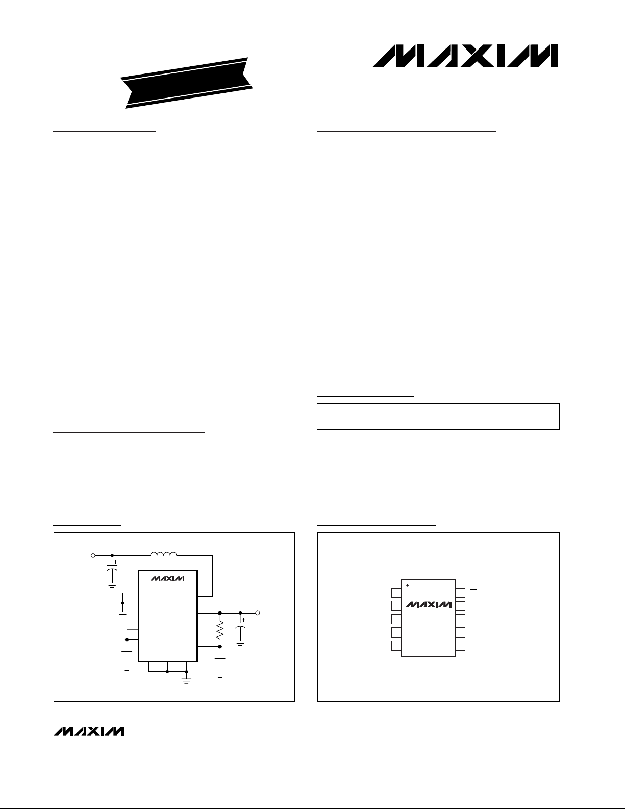
Typical Operating Circuit
19-1660; Rev 1; 1/01
PART
MAX1760EUB -40°C to +85°C
TEMP. RANGE PIN-PACKAGE
10 µMAX
EVALUATION KIT
AVAILABLE
Idle Mode is a trademark of Maxim Integrated Products.
Pin Configuration
Ordering Information
For pricing, delivery, and ordering information, please contact Maxim/Dallas Direct! at
1-888-629-4642, or visit Maxim’s website at www.maxim-ic.com.
INPUT = 0.7V
TO V
OUT
MAX1760
ON
CLK/SEL
ISET
REF
FB GND
LX
POUT
OUT
PGND
V
OUT
800mA
= 3.3V,
TOP VIEW
ISET
REF
GND
1
2
MAX1760
3
4
5
µMAX
ON
10
9
POUT
8
LX
7
PGNDFB
CLK/SELOUT
6
Page 2

MAX1760
0.8A, Low-Noise, 1MHz,
Step-Up DC-DC Converter
2 _______________________________________________________________________________________
ABSOLUTE MAXIMUM RATINGS
ELECTRICAL CHARACTERISTICS
(CLK/SEL = ON = FB = PGND = GND, ISET = REF, OUT = POUT, V
OUT
= 3.6V, TA= 0°C to +85°C. Typical values are at TA=
+25°C, unless otherwise noted.)
Stresses beyond those listed under “Absolute Maximum Ratings” may cause permanent damage to the device. These are stress ratings only, and functional
operation of the device at these or any other conditions beyond those indicated in the operational sections of the specifications is not implied. Exposure to
absolute maximum rating conditions for extended periods may affect device reliability.
ON, OUT, CLK/SEL to GND .....................................-0.3V to +6V
PGND to GND.....................................................................±0.3V
LX to PGND ............................................-0.3V to (V
POUT
+ 0.3V)
POUT to OUT ......................................................................±0.3V
REF, FB, ISET, POUT to GND...................-0.3V to (V
OUT
+ 0.3V)
Continuous Power Dissipation (T
A
= +70°C)
10-Pin µMAX (derate 5.6mW/°C above +70°C) ...........444mW
Operating Temperature Range ...........................-40°C to +85°C
Junction Temperature......................................................+150°C
Storage Temperature Range .............................-65°C to +150°C
Lead Temperature (soldering, 10s) .................................+300°C
DC-DC CONVERTER
Input Voltage Range (Note 1) 0.7 5.5 V
Minimum Startup Voltage (Note 2) I
Temperature Coefficient of Startup Voltage I
Frequency in Startup Mode V
Internal Oscillator Frequency CLK/SEL = OUT 0.8 1 1.2 MHz
Oscillator Maximum Duty Cycle (Note 3) 80 86 90 %
External Clock Frequency Range 0.5 1.2 MHz
Output Voltage
FB Regulation Voltage
FB Input Leakage Current VFB = 1.35V 0.01 100 nA
Load Regulation
Output Voltage Adjust Range 2.5 5.5 V
Output Voltage Lockout Threshold (Note 4) Rising edge 2.00 2.15 2.30 V
ISET Input Leakage Current V
Supply Current in Shutdown V ON = 3.6V 0.1 5 µA
No-Load Supply Current (Note 5) CLK/SEL = GND 100 185 µA
No-Load Supply Current Forced PWM Mode CLK/SEL = OUT 2.5 mA
DC-DC SWITCHES
POUT Leakage Current VLX = 0, V
LX Leakage Current V
Switch On-Resistance
N-Channel Current Limit 1.0 1.25 1.6 A
P-Channel Turn-Off Current CLK/SEL = GND 20 60 120 mA
PARAMETER CONDITIONS MIN TYP MAX UNITS
< 1mA, TA = +25°C 0.9 1.1 V
LOAD
< 1mA -2.3 mV/°C
LOAD
= 1.5V 125 500 1000 kHz
OUT
V
< 0.1V, CLK/SEL = OUT, includes load
FB
regulation for 0 < I
Adjustable output, CLK/SEL = OUT, includes
load regulation for 0 < I
CLK/SEL = OUT, no load to full load
< 1.0A)
(0 < I
LX
= 1.25V ±0.01 ±50 nA
ISET
OUT
= V
LX
ON
N-channel 0.15 0.28
P-channel 0.25 0.45
LX
= 5.5V 0.1 10 µA
= 5.5V 0.1 10 µA
= V
OUT
< 0.55A
< 0.55A
LX
3.17 3.3 3.38 V
1.215 1.240 1.270 V
-1.5 %
Ω
Page 3
MAX1760
0.8A, Low-Noise, 1MHz,
Step-Up DC-DC Converter
_______________________________________________________________________________________ 3
ELECTRICAL CHARACTERISTICS
(CLK/SEL = ON = FB = PGND = GND, ISET = REF, OUT = POUT, V
OUT
= 3.6V, TA= -40°C to +85°C, unless otherwise noted.) (Note 7)
ELECTRICAL CHARACTERISTICS (continued)
(CLK/SEL = ON = FB = PGND = GND, ISET = REF, OUT = POUT, V
OUT
= 3.6V, TA= 0°C to +85°C. Typical values are at TA= +25°C
unless otherwise noted.)
REFERENCES
Reference Output Voltage I
Reference Load Regulation -1µA < IREF < 50µA 5 15 mV
Reference Supply Rejection 2.5V < V
LOGIC INPUTS
CLK/SEL Input Low Level 2.5V ≤ V
CLK/SEL Input High Level 2.5V ≤ V
ON Input Low Level (Note 6)
ON Input High Level (Note 6)
Input Leakage Current CLK/SEL, ON 0.01 1 µA
Minimum CLK/SEL Pulse Width 200 ns
Maximum CLK/SEL Rise/Fall Time 100 ns
PARAMETER CONDITIONS MIN TYP MAX UNITS
= 0 1.230 1.250 1.270 V
REF
< 5V 0.2 5 mV
OUT
≤ 5.5V (0.2)V
OUT
≤ 5.5V (0.8)V
OUT
1.1V ≤ V
1.8V ≤ V
1.1V ≤ V
1.8V ≤ V
≤ 1.8V 0.2
OUT
≤ 5.5V 0.4
OUT
≤ 1.8V V
OUT
≤ 5.5V 1.6
OUT
OUT
OUT
- 0.2
OUT
V
V
V
V
DC-DC CONVERTER
Output Voltage
FB Regulation Voltage
Internal Oscillator Frequency CLK/SEL = OUT 0.75 1.2 MHz
Oscillator Maximum Duty Cycle (Note 3) 80 90 %
Output Voltage Lockout Threshold (Note 4) Rising edge 2.00 2.30 V
Supply Current in Shutdown V ON = 3.6V 5 µA
No-Load Supply Current (Note 5) CLK/SEL = GND 185 µA
DC-DC SWITCHES
Switch On-Resistance
N-Channel Current Limit 1.0 1.6 A
REFERENCE
Reference Output Voltage I
PARAMETER CONDITIONS MIN MAX UNITS
V
< 0.1V, CLK/SEL = OUT, includes load
FB
regulation for 0 < I
Adjustable output, CLK/SEL = OUT, includes
load regulation for 0 < I
N-channel 0.28
P-channel 0.45
= 0 1.230 1.270 V
REF
< 0.55A
LX
< 0.55A
LX
3.17 3.38 V
1.215 1.270 V
Ω
Page 4
MAX1760
0.8A, Low-Noise, 1MHz,
Step-Up DC-DC Converter
4 _______________________________________________________________________________________
Note 1: Operating voltage—since the regulator is bootstrapped to the output, once started the MAX1760 will operate down
to 0.7V input.
Note 2: Startup is tested with the circuit shown in Figure 6.
Note 3: Defines maximum step-up ratio.
Note 4: The regulator is in startup mode until this voltage is reached. Do not apply full load current until the output exceeds 2.3V.
Note 5: Supply current into the OUT pin. This current correlates directly to the actual battery-supply current, but is reduced in
value according to the step-up ratio and efficiency.
Note 6: ON has a hysteresis of approximately 0.15
× V
OUT
.
Note 7: Specifications to -40°C are guaranteed by design and not production tested.
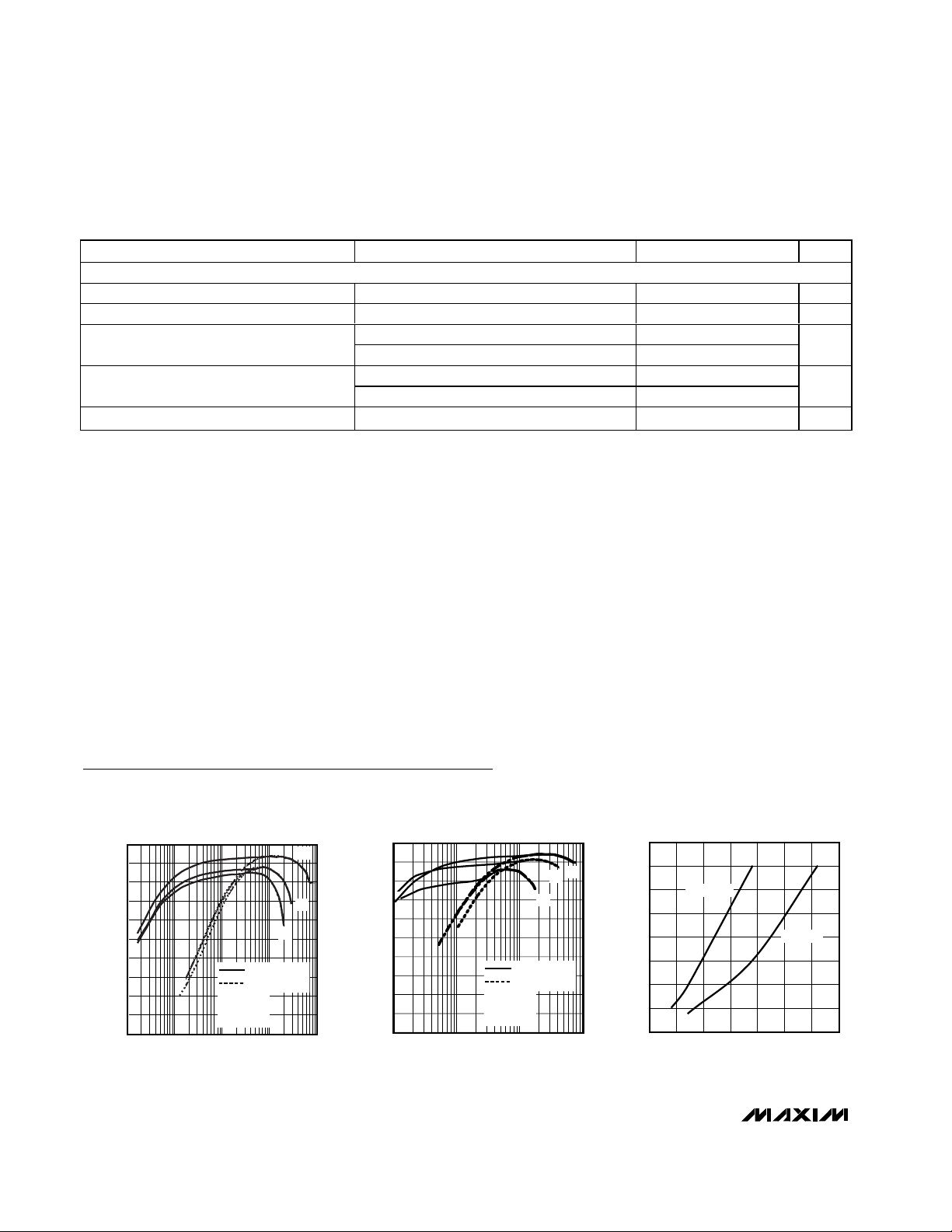
100
0
0.0001 0.001 0.01 0.1 1
EFFICIENCY vs. OUTPUT CURRENT
V
OUT
= 3.3V
20
MAX1760 toc01
OUTPUT CURRENT (A)
EFFICIENCY (%)
40
70
90
60
80
10
30
50
A
B
C
A: VIN = 2.4V
B: V
IN
= 1.2V
C: V
IN
= 0.9V
= AUTO MODE
= FPWM MODE
MAX1760-02
100
0
0.0001 0.001 0.01 0.1 1
EFFICIENCY vs. OUTPUT CURRENT
V
OUT
= 5V
20
OUTPUT CURRENT (A)
EFFICIENCY (%)
40
70
90
60
80
10
30
50
A: VIN = 3.6V
B: V
IN
= 2.4V
C: V
IN
= 1.2V
= AUTO MODE
= FPWM MODE
A
B
C
MAXIMUM OUTPUT CURRENT
vs. INPUT VOLTAGE
MAX1760-03
0.1
1.00.5 1.5 2.0 2.5 3.0 3.5 4.0
0.3
0.2
0.5
0.4
0.8
0.7
0.6
0.9
INPUT VOLTAGE (V)
OUTPUT CURRENT (A)
V
OUT
= 3.3V
V
OUT
= 5V
ELECTRICAL CHARACTERISTICS (continued)
(CLK/SEL = ON = FB = PGND = GND, ISET = REF, OUT = POUT, V
OUT
= 3.6V, TA= -40°C to +85°C, unless otherwise noted.) (Note 7)
Typical Operating Characteristics
(Circuit of Figure 2, VIN= 2.4V, V
OUT
= 3.3V, TA= +25°C, unless otherwise noted.)
LOGIC INPUTS
CLK/SEL Input Low Level 2.5V ≤ V
CLK/SEL Input High Level 2.5V ≤ V
ON Input Low Level (Note 6)
ON Input High Level (Note 6)
Input Leakage Current CLK/SEL, ON 1 µA
PARAMETER CONDITIONS MIN MAX UNITS
≤ 5.5V (0.2)V
OUT
≤ 5.5V (0.8)V
OUT
1.1V ≤ V
1.8V ≤ V
1.1V ≤ V
1.8V ≤ V
≤ 1.8V 0.2
OUT
≤ 5.5V 0.4
OUT
≤ 1.8V V
OUT
≤ 5.5V 1.6
OUT
OUT
+ 0.2
OUT
OUT
V
V
V
V
Page 5

MAX1760
0.8A, Low-Noise, 1MHz,
Step-Up DC-DC Converter
_______________________________________________________________________________________ 5
Typical Operating Characteristics (continued)
(Circuit of Figure 2, VIN= 2.4V, V
OUT
= 3.3V, TA= +25°C, unless otherwise noted.)
INPUT CURRENT (mA)
NO-LOAD BATTERY CURRENT
vs. INPUT VOLTAGE
2.5
2.0
1.5
1.0
0.5
V
= 3.3V
OUT
0.0
021345
INPUT VOLTAGE (V)
V
= 5V
OUT
STARTUP VOLTAGE
vs. OUTPUT CURRENT
3.0
A = +85°C
B = +25°C
2.5
C = -40°C
2.0
A
1.5
1.0
STARTUP VOLTAGE (V)
0.5
CIRCUIT OF FIGURE 6
0.0
0.001 0.01 0.1 1
C
B
OUTPUT CURRENT (A)
MAX1760-04
SHUTDOWN CURRENT (nA)
TOTAL SHUTDOWN CURRENT
+ I
(I
10
1
0.1
02146
) vs. INPUT VOLTAGE
LX
OUT
INPUT VOLTAGE (V)
35
PEAK INDUCTOR CURRENT vs. V
1.4
1.2
MAX1760-07
1.0
0.8
0.6
0.4
PEAK INDUCTOR CURRENT (A)
0.2
0.0
0.1 0.5 0.70.3 0.9 1.1 1.3
(V)
V
ISET
ISET
MAX1760-05
MAX1760-08
INTERNAL OSCILLATOR
FREQUENCY vs. TEMPERATURE
1.20
1.15
1.10
1.05
1.00
0.95
FREQUENCY (MHz)
0.90
0.85
0.80
0.75
-40 10-15 35 60 85
TEMPERATURE (°C)
HEAVY-LOAD SWITCHING WAVEFORMS
A
B
C
0V
A = LX PIN, 5V/div
B = INDUCTOR CURRENT, 200mA/div
C = OUTPUT RIPPLE, 50mV/div AC-COUPLED
t = 400ns/div
MAX1760-06
MAX1760-09
LIGHT-LOAD SWITCHING WAVEFORMS
A
B
C
t = 400ns/div
A = LX PIN, 5V/div
B = INDUCTOR CURRENT, 200mA/div
C = OUTPUT RIPPLE, 50mV/div, AC-COUPLED
MAX1760-10
LOAD-TRANSIENT RESPONSE
A
B
t = 200ms/div
= 1.1V, V
V
IN
OUT
, 100mA/div
A = I
OUT
, 50mV/div, AC-COUPLED
B = V
OUT
= 3.3V, I
= 0 AND 0.2A
OUT
MAX1760-11
LINE-TRANSIENT RESPONSE
A
B
= 2.4V TO 1.4V, I
V
IN
A = VIN, 1V/div
, 5mA/div, AC-COUPLED
B = V
OUT
400µs/div
OUT
MAX1760-12
= 70mA
Page 6

MAX1760
0.8A, Low-Noise, 1MHz,
Step-Up DC-DC Converter
6 _______________________________________________________________________________________
Pin Description
Typical Operating Characteristics (continued)
(Circuit of Figure 2, VIN= 2.4V, V
OUT
= 3.3V, TA= +25°C, unless otherwise noted.)
Power Output. P-channel synchronous-rectifier source.
POUT9
Shutdown Control Input. When ON = high, the IC is in shutdown. Connect ON to GND for normal operation.ON
10
IC Power, Supplied from the Output. Bypass to GND with a 0.68µF ceramic capacitor, and connect to POUT
with a series 4.7Ω resistor (Figure 2).
OUT5
Clock Input for the DC-DC Converter. Also serves to program operating mode of switcher as follows:
CLK/SEL = LO: Normal operation—operates at a fixed frequency, automatically switching to low-power
mode if load is minimized.
CLK/SEL = HI: Forced PWM mode—operates in low-noise, constant-frequency mode at all loads.
CLK/SEL = Clocked: Forced PWM mode with the internal oscillator synchronized to CLK in 500kHz to
1200kHz range.
CLK/SEL6
Source of N-Channel Power MOSFET SwitchPGND7
Inductor ConnectionLX8
DC-DC Converter Feedback Input. To set fixed output voltage of +3.3V, connect FB to ground. For
adjustable output of 2.5V to 5.5V, connect to a resistive divider from OUT to GND. FB set point = 1.24V.
FB4
Ground. Connect to PGND with short trace. GND3
PIN
1.250V Voltage Reference Bypass. Connect a 0.22µF ceramic bypass capacitor to GND. Up to 50µA of
external load current is allowed.
REF2
N-Channel Current-Limit Control. For maximum current limit, connect to REF. To reduce current, supply a
voltage between REF and GND by means of a resistive voltage-divider. If soft-start is desired, connect a
capacitor from ISET to GND. When ON = high, or V
REF
<80% of nominal value, an on-chip 100kΩ switched
resistor discharges this pin to GND.
ISET1
FUNCTIONNAME
NOISE SPECTRUM
16
TURN-ON WAVEFORMS
NO SOFT-START COMPONENTS
SOFT-START WAVEFORMS
= 500kΩ, CSS = 0.1µF
R
SS
12
)
8
RMS
4
NOISE (mV
0
FREQUENCY (MHz)
MAX1760-13
1010.1
A
B
C
OV
t = 2ms/div
A = ON, 5V/div
B = INPUT CURRENT, 500mA/div
, 2V/div
C = V
OUT
MAX1760-14
A
B
C
0V
2.00ms/div
A = ON, 5V/div
B = INPUT CURRENT, 100mA/div
, 2V/div
C = V
OUT
MAX1760-15
Page 7

MAX1760
0.8A, Low-Noise, 1MHz,
Step-Up DC-DC Converter
_______________________________________________________________________________________ 7
Detailed Description
The MAX1760 is a highly efficient, low-noise power supply for portable RF and hand-held instruments. It combines a boost switching regulator, N-channel power
MOSFET, P-channel synchronous rectifier, precision
reference, and shutdown control (Figure 1).
The DC-DC converter boosts a 1-cell to 3-cell battery
voltage input to a fixed 3.3V or adjustable voltage
between 2.5V and 5.5V. An external Schottky diode is
required for output voltages greater than 4V. The
MAX1760 guarantees startup with an input voltage as
low as 1.1V and remains operational down to an input
of just 0.7V. It is optimized for use in cellular phones
and other applications requiring low noise and low quiescent current for maximum battery life. It features
fixed-frequency operation at medium and heavy loads,
but at light loads, switches only as needed for optimum
efficiency. This device is also capable of constant-frequency (1MHz), low-noise PWM operation at all load
currents, or frequency-synchronized PWM operation
when connected to an external clock. Table 1 lists
some typical outputs. Shutdown reduces quiescent current to just 1µA. Figure 2 shows the standard application circuit for the MAX1760.
Step-Up Converter
During DC-DC converter operation, the internal N-channel MOSFET switch turns on for the first part of each
cycle, allowing current to ramp up in the inductor and
store energy in a magnetic field. During the second
part of each cycle, the MOSFET turns off and inductor
current flows through the synchronous rectifier to the
OUT
Figure 1. Functional Diagram
Figure 2. Standard Application Circuit
UNDERVOLTAGE LOCKOUT
IC POWER
2.15V
STARTUP
EN
ON
OSCILLATOR
Q
CONTROLLER
D
PCH
POUT
ON RDY
REFERENCE
REF
GND
CLK/SEL
FB
ISET
1.25V
MAX1760
REF GND
LX
PGND
4.7Ω
0.68µF
EN
OSCILLATOR
CLK/SEL
1MHz
V
IN
MODE
= 2.4V
0.22µF
33µF
EN
OSCOSC
MODE
FB
ON
CLK/SEL
ISET
REF
FB
ISET
3.3µH
MAX1760
NCH
LX
POUT
OUT
PGNDGND
V
OUT
800mA
100µF
= 3.3V,
Page 8

MAX1760
0.8A, Low-Noise, 1MHz,
Step-Up DC-DC Converter
8 _______________________________________________________________________________________
output filter capacitor and the load. As the energy
stored in the inductor is depleted, the current ramps
down and the synchronous rectifier turns off. At light
loads, the device operates at fixed frequency or only as
needed to maintain regulation, depending on the
CLK/SEL setting (Table 2).
Normal Operation
Pulling CLK/SEL low selects the MAX1760’s normal
operating mode. In this mode, the device operates in
PWM when driving medium-to-heavy loads, and automatically switches to PFM if the load requires less
power. PFM operation allows higher efficiency than
PWM under light load conditions.
Forced PWM Operation
When CLK/SEL is high, the MAX1760 operates in a lownoise PWM-only mode. During forced PWM operation,
the MAX1760 switches at a constant frequency (1MHz),
and modulates the MOSFET switch pulse width to control the power transferred per cycle to regulate the output voltage. Switching harmonics generated by
fixed-frequency operation are consistent and easily filtered. See the Noise Spectrum plot in the Typical
Operating Characteristics.
Synchronized PWM Operation
The MAX1760 can be synchronized in PWM mode to an
external frequency of 500kHz to 1.2MHz by applying an
external clock signal to CLK/SEL. This allows interference to be minimized in wireless applications. The synchronous rectifier is active during synchronized PWM
operation.
Synchronous Rectifier
The MAX1760 features an internal, P-channel synchronous rectifier to enhance efficiency. Synchronous rectification provides 5% improved efficiency over similar
nonsynchronous boost regulators. In PWM mode, the
synchronous rectifier is turned on during the second
half of each switching cycle. In low-power mode, an
internal comparator turns on the synchronous rectifier
when the voltage at LX exceeds the boost regulator
output, and turns it off when the inductor current drops
below 60mA. When setting output voltages greater than
4V, an external 0.5A Schottky diode must be connected
in parallel with the on-chip synchronous rectifier.
Low-Voltage Startup Oscillator
The MAX1760 uses a CMOS, low-voltage startup oscillator for a 1.1V guaranteed minimum startup input voltage. At startup, the low-voltage oscillator switches the
N-channel MOSFET until the output voltage reaches
2.15V. Above this level, the normal boost-converter
feedback and control circuitry take over. Once the
device is in regulation, it can operate down to 0.7V
input since internal power for the IC is bootstrapped
from the output through OUT. Do not apply full load
until the output exceeds 2.3V.
Shutdown
The MAX1760 has a shutdown mode that reduces quiescent current to 0.1µA. During shutdown (ON = high),
the reference and all feedback and control circuitry are
off. During shutdown, the output voltage is one diode
drop below the input voltage.
Table 1. Typical Available Output Current
5.03.63 750
3.32.4
2
3.31.21
OUTPUT VOLTAGE
(V)
INPUT VOLTAGE
(V)
NUMBER OF NiCd/NiMH
CELLS
800
350
OUTPUT CURRENT
(mA)
5.02.4 500
Table 2. Selecting the Operating Mode
CLK/SEL MODE FEATURES
0 Normal Operation High efficiency at all loads. Fixed frequency at all but light loads.
1 Forced PWM
Low noise, fixed frequency at all loads.
External Clock
500kHz to 1.2MHz
Synchronized PWM
Low noise, fixed frequency at all loads.
Page 9

Reference
The MAX1760 has an internal 1.250V ±1% reference.
Connect a 0.22µF ceramic bypass capacitor from REF
to GND within 0.2in (5mm) of the REF pin. REF can
source up to 50µA of external load current.
Design Procedure
Setting the Output Voltages
For a fixed 3.3V output, connect FB to GND. To set
other output voltages between 2.5V and 5.5V, connect
a resistor voltage-divider to FB from OUT to GND
(Figure 3). The input bias current into FB is <20nA,
allowing large-value divider resistors without sacrificing
accuracy. Connect the resistor voltage-divider as close
to the IC as possible, within 0.2in (5mm) of FB. Choose
R2 of 270kΩ or less, then calculate R1 using:
where V
FB
, the boost-regulator feedback set point, is
1.24V.
Setting the Switch Current Limit
and Soft-Start
The ISET pin adjusts the inductor current limit and
implements soft-start. With ISET connected to REF, the
inductor current limits at 1.25A. With ISET connected to
a resistive divider set from REF to GND, the current limit
is reduced according to:
Implement soft-start by placing a resistor from ISET to
REF and a capacitor from ISET to GND. In shutdown,
ISET is discharged to GND through an on-chip 100kΩ
resistor. At power-up, ISET is 0V and the LX current is
zero. As the capacitor voltage rises, the current
increases and the output voltage rises. The soft-start
I 1.25A
V
1.25V
LIM
ISET
=
MAX1760
0.8A, Low-Noise, 1MHz,
Step-Up DC-DC Converter
_______________________________________________________________________________________ 9
Figure 3. Connecting Resistors for External Feedback
Figure 4. Soft-Start with Maximum Switch Limit Current
Figure 5. Soft-Start with Reduced Switch Current Limit
= 2.4V
V
IN
33µF
0.22µF
3.3µH
CLK/SEL
POUT
OUT
FB
LX
V
OUT
0.68µF
R1 = R2
= 1.24V
V
FB
100µF
V
OUT
- 1
( )
V
FB
4.7Ω
R1
R2
ON
MAX1760
ISET
REF
PGND GND
REF
0.22µF
R
SS
C
MAX1760
ISET
SS
= 1.25A
I
LIM
tSS = RSSC
R
≥ 470k
SS
SS
R1 R2
V
=−
V
OUT
FB
1
0.22µF
R
SS2
REF
I
= 1.25A
R
SS1
C
MAX1760
ISET
SS
LIM
tSS = (R
R
SS1
≥ 470k
( )
R
R
SS1
SS2
II
R
SS2
SS1 + RSS2
) C
SS
Page 10

MAX1760
time constant is:
where RSS≥ 470k.
Placing a capacitor across the lower resistor of the current-limiting resistive divider provides both current-limit
and soft-start features simultaneously (Figures 4 and 5).
Inductor Selection
The MAX1760’s high switching frequency allows the
use of a small 3.3µH surface-mount inductor. The chosen inductor should generally have a saturation current
rating exceeding the N-channel switch current limit;
however, it is acceptable to bias the inductor current
into saturation by as much as 20% if a slight reduction
in efficiency is acceptable. Lower current-rated inductors may be used if ISET is employed to reduce the
peak inductor current (see Setting the Switch Current
Limit and Soft-Start). For high efficiency, choose an
inductor with a high-frequency ferrite core material to
reduce core losses. To minimize radiated noise, use a
toroid or shielded inductor. See Table 3 for suggested
components and Table 4 for a list of component suppliers. Connect the inductor from the battery to the LX pin
as close to the IC as possible.
External Diode
For output voltages greater than 4V, an external
Schottky diode must be connected from LX to POUT, in
parallel with the on-chip synchronous rectifier (Figure
6). The diode should be rated for 0.5A. Representative
devices are Motorola MBR0520L, Nihon EP05Q03L, or
generic 1N5817. This external diode is also recommended for applications that must start with input voltages at or below 1.8V. The Schottky diode carries
current during startup and after the synchronous rectifier turns off; thus, its current rating only needs to be
500mA. Connect the diode as close to the IC as possible. Do not use ordinary rectifier diodes; their slow
switching speeds and long reverse-recovery times render them unacceptable. For circuits that do not require
startup with inputs below 1.8V, and have an output of
4V or less, no external diode is needed.
Input and Output Filter Capacitors
Choose input and output filter capacitors that will service the input and output peak currents with acceptable voltage ripple. Choose input capacitors with
working voltage ratings over the maximum input volt-
tRC
SS SS SS
=
0.8A, Low-Noise, 1MHz,
Step-Up DC-DC Converter
10 ___________________________________________________
Table 3. Component Selection Guide
Sanyo POSCAP series
Sumida CDRH5D18
Kemet T510 series
Coilcraft LPT3305
—
Sumida CD43
Surface Mount
AVX TPS seriesCoilcraft DS3316P
CAPACITORSINDUCTORSPRODUCTION METHOD
—
Motorola MBR0520L
—
EIC SB series
DIODES
Table 4. Component Suppliers
USA: 916-941-0712EIC
USA: 847-639-6400Coilcraft
USA: 847-956-0666
Japan: 011-81-3-3667-3302
Sumida
USA: 843-448-9411AVX
PHONESUPPLIER
USA: 408-629-4789
Japan: 81-45-474-7030
Motorola
USA: 810-287-2536Kemet
Note: Please indicate that you are using the MAX1760 when
contacting these component suppliers.
Figure 6. Connection with External Schottky Diode for Output
Voltages Greater than 4V, or to Assist Low-Voltage Startup
V
= 0.7V
IN
TO VOUT
33µF
0.22µF
3.3µH
CLK/SEL
ON
MAX1760
ISET
REF
PGND GND
POUT
OUT
FB
MRB0520L
LX
4.7Ω
0.68µF
100µF
V
OUT
Page 11

age, and output capacitors with working voltage ratings
higher than the output.
The input filter capacitor reduces peak currents drawn
from the input source and also reduces input switching
noise. The input voltage source impedance determines
the required value of the input capacitor. When operating directly from one or two NiMH cells placed close to
the MAX1760, use a single 33µF low-ESR input filter
capacitor. With higher impedance batteries, such as
alkaline and Li+, a higher value input capacitor may
improve efficiency.
The output filter capacitor reduces output ripple voltage
and provides the load with transient peak currents
when necessary. For the output, a 100µF, low-equivalent-series-resistance (ESR) capacitor is recommended
for most applications.
Sanyo POSCAP, Panasonic SP/CB, and Kemet T510
are good low-ESR capacitors. Low-ESR tantalum
capacitors offer a good tradeoff between price and
performance. Do not exceed the ripple current ratings
of tantalum capacitors. Avoid aluminum electrolytic
capacitors; their high ESR typically results in higher
output ripple voltage.
Other External Components
Two ceramic bypass capacitors are required for proper
operation. Bypass REF to GND with 0.22µF. Also,
bypass OUT to GND with a 0.68µF ceramic capacitor,
and connect OUT to POUT with a 4.7Ω resistor. Each of
these components should be placed as close to its
respective IC pins as possible, within 0.2in (5mm).
Table 4 lists suggested suppliers.
Layout Considerations
High switching frequencies and large peak currents
make PC board layout a critical part of design. Poor
design will cause excessive EMI and ground bounce,
both of which can cause instability or regulation errors
by corrupting the voltage and current feedback signals.
Power components—such as the inductor, converter
IC, filter capacitors, and output diode—should be
placed as close together as possible, and their traces
should be kept short, direct, and wide. Keep the voltage feedback network very close to the IC, within 0.2in
(5mm) of the FB pin. Keep noisy traces, such as those
from the LX pin, away from the voltage feedback network and guarded from them using grounded copper.
Refer to the MAX1760 EV kit for a full PC board example.
MAX1760
0.8A, Low-Noise, 1MHz,
Step-Up DC-DC Converter
______________________________________________________________________________________ 11
TRANSISTOR COUNT: 1361
Chip Information
Page 12

MAX1760
0.8A, Low-Noise, 1MHz,
Step-Up DC-DC Converter
Maxim cannot assume responsibility for use of any circuitry other than circuitry entirely embodied in a Maxim product. No circuit patent licenses are
implied. Maxim reserves the right to change the circuitry and specifications without notice at any time.
12 ____________________Maxim Integrated Products, 120 San Gabriel Drive, Sunnyvale, CA 94086 408-737-7600
© 2001 Maxim Integrated Products Printed USA is a registered trademark of Maxim Integrated Products.
Package Information
10LUMAX.EPS
 Loading...