

Page 1
General Description
The MAX1759 is a buck/boost regulating charge pump
that generates a regulated output voltage from a single
lithium-ion (Li+) cell, or two or three NiMH or alkaline
cells for small hand-held portable equipment. The
MAX1759 operates over a wide +1.6V to +5.5V input
voltage range and generates a fixed 3.3V or adjustable
(2.5V to 5.5V) output (Dual Mode™). Maxim’s unique
charge-pump architecture allows the input voltage to be
higher or lower than the regulated output voltage.
Despite its high 1.5MHz operating frequency, the
MAX1759 maintains low 50µA quiescent supply current.
Designed to be an extremely compact buck/boost converter, this device requires only three small ceramic
capacitors to build a complete DC-DC converter capable of generating a guaranteed 100mA (min) output
current from a +2.5V input. For added flexibility, the
MAX1759 also includes an open-drain power-OK
(POK) output that signals when the output voltage is in
regulation.
The MAX1759 is available in a space-saving 10-pin
µMAX package that is 1.09mm high and half the size of
an 8-pin SO.
Applications
Li+ Battery-Powered Applications
Miniature Equipment
Backup Battery Boost Converters
Translators
Features
♦ Regulated Output Voltage (Fixed 3.3V or
Adjustable 2.5V to 5.5V)
♦ 100mA Guaranteed Output Current
♦ +1.6V to +5.5V Input Voltage Range
♦ Low 50µA Quiescent Supply Current
♦ 1µA Shutdown Mode
♦ Load Disconnected from Input in Shutdown
♦ High 1.5MHz Operating Frequency
♦ Uses Small Ceramic Capacitors
♦ Short-Circuit Protection and Thermal Shutdown
♦ Small 10-Pin µMAX Package
MAX1759
Buck/Boost Regulating
Charge Pump in µMAX
________________________________________________________________ Maxim Integrated Products 1
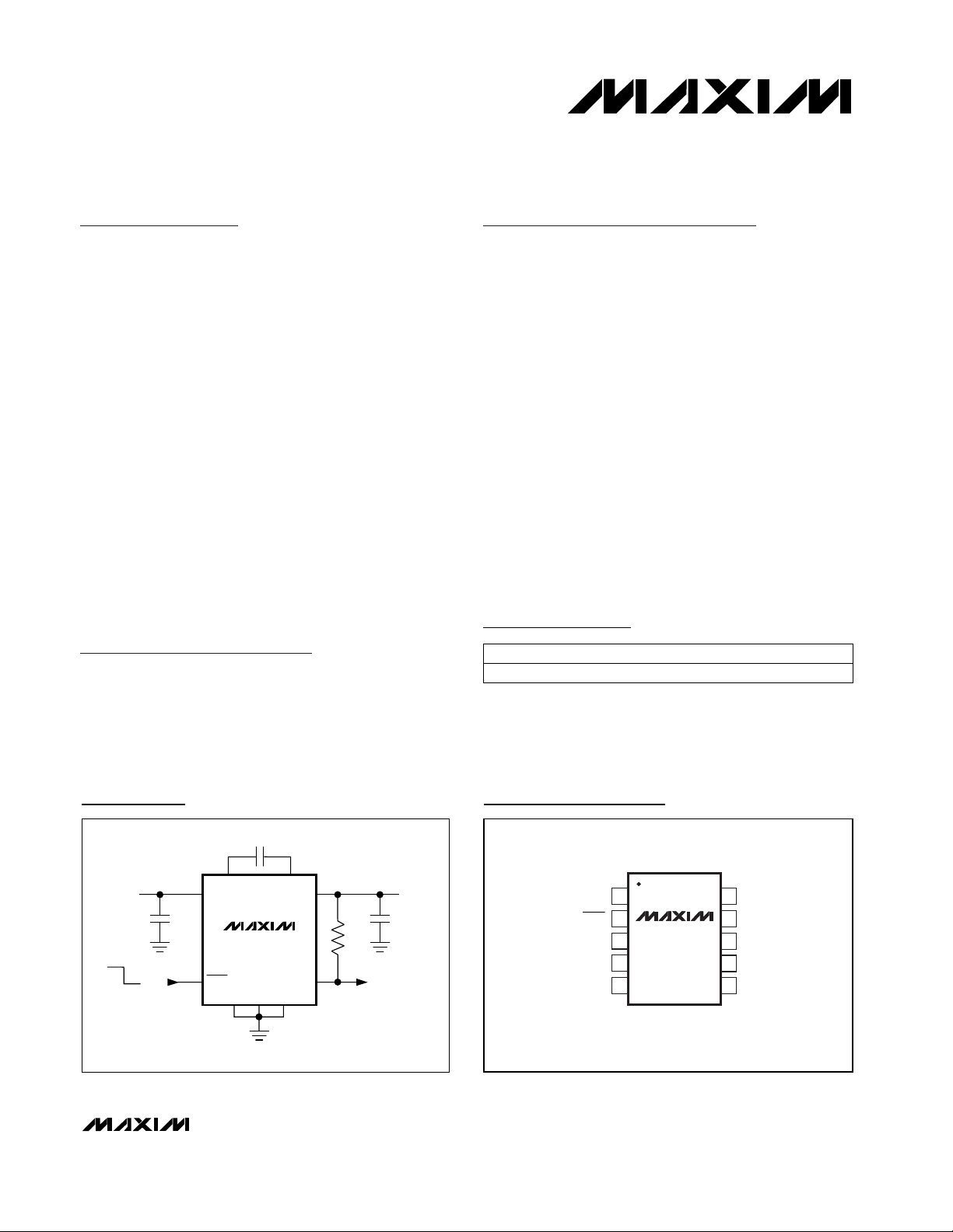
Typical Operating Circuit
19-1600; Rev 1; 6/00
PART
MAX1759EUB -40°C to +85°C
TEMP. RANGE PIN-PACKAGE
10 µMAX
Pin Configuration
Ordering Information
Dual Mode is a trademark of Maxim Integrated Products.
For price, delivery, and to place orders, please contact Maxim Distribution at 1-888-629-4642,
or visit Maxim’s website at www.maxim-ic.com.
C
X
IN
+1.6V TO +5.5V
C
IN
ON
OFF
CXN CXP
IN
MAX1759
SHDN
OUT
POK
PGNDGNDFB
OUT
3.3V AT 100mA
POWER OK
TOP VIEW
1
POK
C
OUT
SHDN
2
3
IN
4
5
10
FB
9
MAX1759
µMAX
OUT
8
CXP
7
CXNIN
PGNDGND
6
Page 2
MAX1759
Buck/Boost Regulating
Charge Pump in µMAX
2 _______________________________________________________________________________________
ABSOLUTE MAXIMUM RATINGS
ELECTRICAL CHARACTERISTICS
(Circuit of Figure 1, VIN= V
SHDN
= 2V, FB = PGND = GND, CIN= 10µF, CX= 0.33µF, C
OUT
= 10µF, TA= 0°C to +85°C, unless oth-
erwise noted. Typical values are at T
A
= +25°C.)
Stresses beyond those listed under “Absolute Maximum Ratings” may cause permanent damage to the device. These are stress ratings only, and functional
operation of the device at these or any other conditions beyond those indicated in the operational sections of the specifications is not implied. Exposure to
absolute maximum rating conditions for extended periods may affect device reliability.
IN, OUT, FB, POK, SHDN to GND............................-0.3V to +6V
PGND to GND.....................................................................±0.3V
CXN to GND ................................................-0.3V to (V
IN
+ 0.3V)
CXP to GND................-0.3V to (the greater of V
IN
or V
OUT
) + 1V
OUT Short to GND .........................................................Indefinite
Continuous Power Dissipation (T
A
= +70°C)
10-Pin µMAX (derate 5.6mW/°C above +70°C) .........444mW
Operating Temperature Range .......................... -40°C to +85°C
Junction Temperature......................................................+150°C
Storage Temperature Range .............................-65°C to +150°C
Lead Temperature (soldering, 10s) ................................ +300°C
I
LOAD,MAX
Thermal Shutdown Hysteresis
20
°C
Efficiency
90
%VIN= 3.6V, I
LOAD
= 10mA
PARAMETER SYMBOL MIN TYP MAX UNITS
Transient Load Current
200
mA
Maximum Output Current
100
mA
3.17 3.3 3.43
Output Voltage V
OUT
3.17 3.3 3.43
V
Quiescent Supply Current I
Q
50 90
85 180
µA
Shutdown Supply Current I
Q,SHDN
15
µA
Leakage Current into OUT in
Shutdown
15
µA
Input Undervoltage Lockout
Voltage
Input Voltage Range V
IN
1.6 5.5
V
V
UVLO
0.6 1.0 1.4
V
Output Voltage Adjustment Range
2.5 5.5
V
SHDN Logic Input Voltage
V
IL
0.25 · V
IN
V
V
IH
0.7 · V
IN
SHDN Input Leakage Current
I
SHDN
-1 1
µA
FB Regulation Voltage V
FB
1.205 1.235 1.265
V
FB Input Current
25 200
nA
FB Dual-Mode Threshold
100 50
mV
200 100
mV
POK Trip Voltage
1.0 1.1 1.2
V
POK Output Low Voltage V
OL
5100
mV
POK Leakage Current
0.01 0.2
µA
Switching Frequency f
OSC
1.2 1.5 1.8
MHz
Output Short-Circuit Current
110
mA
Thermal Shutdown Temperature
160
°C
CONDITIONS
1.6V ≤ VIN≤ 5.5V
I
LOAD
≤ 100mA (RMS)
1.6V ≤ VIN≤ 5.5V
2.5V ≤ VIN≤ 5.5V
2.5V ≤ VIN≤ 5.5V, 1mA ≤ I
LOAD
≤ 100mA
2V ≤ VIN≤ 5.5V, 1mA ≤ I
LOAD
≤ 50mA
VIN= V
SHDN
= 4V, VFB= 0, stepping down
VIN= V
SHDN
= 2V, VFB= 0, stepping up
V
SHDN
= 5.5V
VIN= 1.65V, V
OUT
= 3.3V
1.6V ≤ VIN≤ 5.5V, V
SHDN
= 0
VIN= 2V, V
OUT
= 3.3V, V
SHDN
= 0
VFB= 1.27V
Internal feedback
External feedback
Falling edge at FB
I
SINK
= 0.5mA, VIN= 2V
V
POK
= 5.5V, VFB= 1.27V
1.6V ≤ VIN≤ 5.5V
1.6V ≤ VIN≤ 5.5V, VFB= 1V
V
OUT
= 0, 2.5V ≤ VIN≤5.5V, foldback current limit
Rising temperature
Page 3
MAX1759
Buck/Boost Regulating
Charge Pump in µMAX
_______________________________________________________________________________________ 3
ELECTRICAL CHARACTERISTICS
(Circuit of Figure 1, VIN= V
SHDN
= 2V, FB = PGND = GND, CIN= 10µF, CX= 0.33µF, C
OUT
= 10µF, TA= -40°C to +85°C, unless oth-
erwise noted.) (Note 1)
Note 1: Specifications to -40°C are guaranteed by design and are not production tested.
PARAMETER
SYMBOL MIN MAX UNITS
Quiescent Supply Current I
Q
90
Maximum Output Current I
LOAD,MAX
100
mA
Output Voltage Adjustment
Range
2.5 5.5
V
3.15 3.45
V
180
µA
Shutdown Supply Current I
Q,SHDN
6
µA
Leakage Current into OUT in
Shutdown
5
µA
SHDN Input Logic Voltage
V
IL
0.2 · V
IN
V
Input Undervoltage Lockout
Voltage
Input Voltage Range V
IN
1.6 5.5
V
V
UVLO
0.6 1.4
V
Output Voltage V
OUT
3.15 3.45
V
V
IH
0.7 · V
IN
V
SHDN Input Leakage Current
I
SHDN
-1 1
µA
FB Regulation Voltage V
FB
1.205 1.265
V
FB Input Bias Current
200
nA
FB Dual Mode Threshold
40
mV
200
mV
POK Trip Voltage
1.0 1.2
V
POK Output Low Voltage V
OL
100
mV
POK Leakage Current
0.2
µA
Switching Frequency f
OSC
1.1 1.9
MHz
CONDITIONS
1.6V ≤ VIN≤ 5.5V
VIN= V
SHDN
= 4V, VFB= 0
V
SHDN
= 5.5V
2.5V ≤ VIN≤ 5.5V
1.6V ≤ VIN≤ 5.5V
2.5V ≤ VIN≤ 5.5V, 0 ≤ I
LOAD
≤ 100mA
VIN= V
SHDN
= 2.5V, VFB= 0
1.6V ≤ VIN≤ 5.5V, V
SHDN
= 0
VIN= 1.65V, V
OUT
= 3.3V
VFB= 1.27V
VIN= 2V, V
OUT
= 3.3V, V
SHDN
= 0
1.6V ≤ VIN≤ 5.5V
Internal feedback
External feedback
Falling edge at FB
I
SINK
= 0.5mA, VIN= 2V
V
POK
= 5.5V
1.6V ≤ VIN≤ 5.5V, VFB= 1V
2V ≤ VIN≤ 5.5V, 0 ≤ I
LOAD
≤ 50mA
Page 4
MAX1759
Buck/Boost Regulating
Charge Pump in µMAX
4 _______________________________________________________________________________________
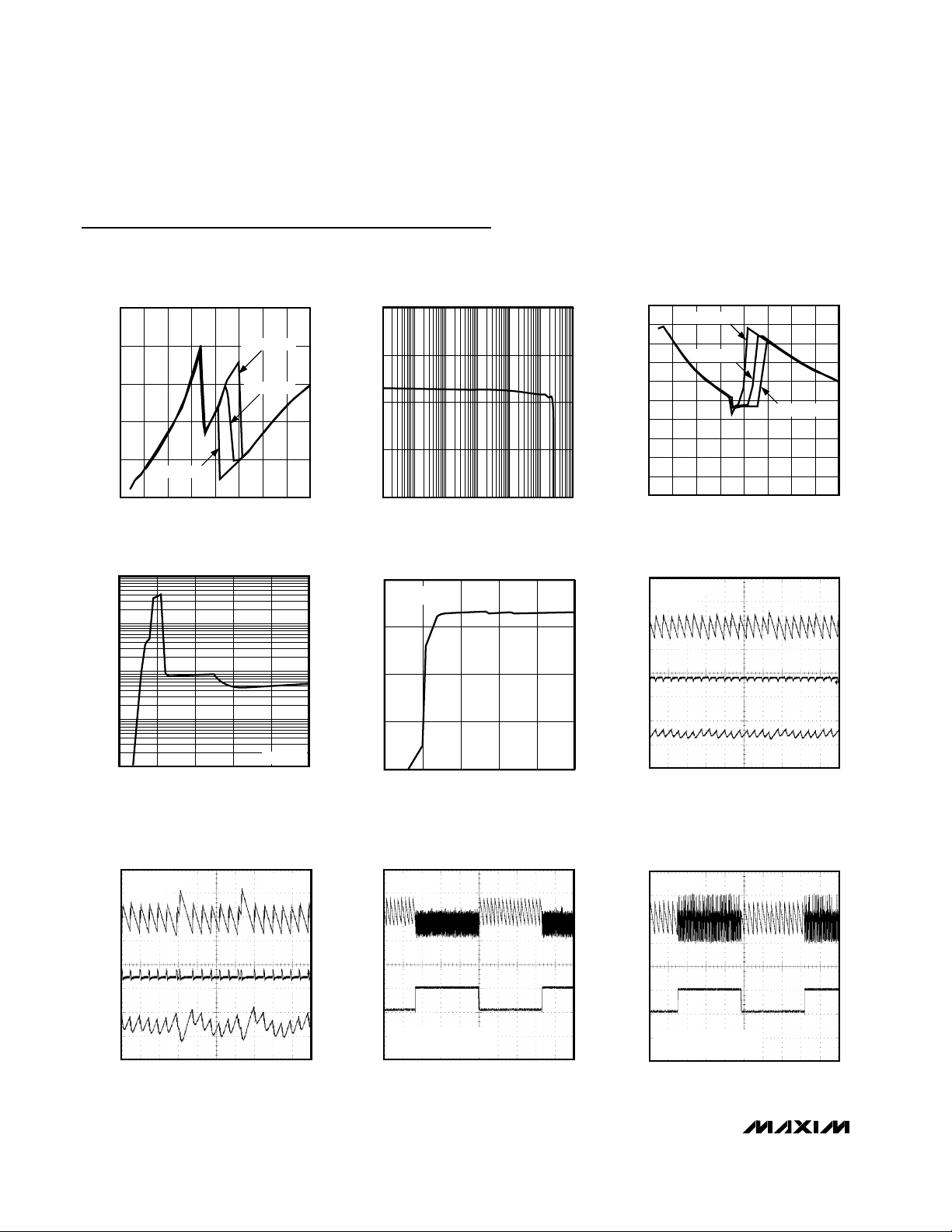
Typical Operating Characteristics
(Circuit of Figure 1, CIN= 10µF, CX= 0.33µF, C
OUT
= 10µF, V
OUT
= 3.3V, VIN= 2.5V, TA= +25°C, unless otherwise noted.)
0
20
60
40
80
100
1.5 2.5 3.5 4.5 5.5
OUTPUT VOLTAGE RIPPLE
vs. INPUT VOLTAGE
MAX1759 toc01
INPUT VOLTAGE (V)
OUTPUT VOLTAGE RIPPLE (mV)
I
OUT
= 10mA
I
OUT
= 50mA
I
OUT
= 100mA
OUTPUT VOLTAGE vs. LOAD CURRENT
MAX1759 toc02
LOAD CURRENT (mA)
OUTPUT VOLTAGE (V)
3.40
3.20
3.25
3.30
3.35
0.001 1 10 1000.01 0.1 1000
0
20
10
40
30
60
50
70
90
80
100
1.5 2.5 3.5 4.5 5.5
EFFICIENCY vs. INPUT VOLTAGE
MAX1759 toc03
INPUT VOLTAGE (V)
EFFICIENCY (%)
I
OUT
= 10mA
I
OUT
= 50mA
I
OUT
= 100mA
0.5 1.5 2.5 3.5 4.5 5.5
QUIESCENT CURRENT
vs. INPUT VOLTAGE
MAX1759 toc04
INPUT VOLTAGE (V)
QUIESCENT CURRENT (µA)
10,000
1
10
100
1000
NO LOAD
4
3
2
1
0
0.5 2.51.5 3.5 4.5 5.5
STARTUP INPUT VOLTAGE
(V
OUT
< VIN)
MAX1759 toc05
INPUT VOLTAGE (V)
OUTPUT VOLTAGE (V)
R
LOAD
= 33Ω
1
3
2
5µs/div
TYPICAL SWITCHING WAVEFORMS
(V
OUT
< VIN)
MAX1759 toc06
CH1: V
OUT
, 20mV/div, AC-COUPLED
CH2: V
CXP
, 5V/div
CH3: V
IN
, 50mV/div, AC-COUPLED
R
LOAD
= 33Ω
V
IN
= 4.2V
1
3
2
5µs/div
TYPICAL SWITCHING WAVEFORMS
(V
OUT
> VIN)
MAX1759 toc07
CH1: V
OUT
, 20mV/div, AC-COUPLED
CH2: V
CXP
, 5V/div
CH3: V
IN
, 50mV/div, AC-COUPLED
R
LOAD
= 33Ω
V
IN
= 2.5V
1
2
100µs/div
LOAD-TRANSIENT RESPONSE
(V
OUT
< VIN)
MAX1759 toc08
CH1: V
OUT
, 20mV/div, AC-COUPLED
CH2: I
OUT
, 100mA/div
LOAD STEP: 10mA TO 100mA
V
IN
= 4.2V
1
2
100µs/div
LOAD-TRANSIENT RESPONSE
(V
OUT
> VIN)
MAX1759 toc09
CH1: V
OUT
, 20mV/div, AC-COUPLED
CH2: I
OUT
, 100mA/div
LOAD STEP: 10mA TO 100mA
V
IN
= 2.5V
Page 5

MAX1759
Buck/Boost Regulating
Charge Pump in µMAX
_______________________________________________________________________________________ 5
Typical Operating Characteristics (continued)
(Circuit of Figure 1, CIN= 10µF, CX= 0.33µF, C
OUT
= 10µF, V
OUT
= 3.3V, VIN= 2.5V, TA= +25°C, unless otherwise noted.)
NAME FUNCTION
1 POK
Open-Drain Power-OK Output. POK is high impedance when output voltage is in regulation. POK sinks current
when V
FB
falls below 1.1V. Connect a 10kΩ to 1MΩ pull-up resistor from POK to V
OUT
for a logic signal.
Ground POK or leave unconnected if not used. POK is high impedance in shutdown.
2
SHDN
Shutdown Input. Drive high for normal operation; drive low for shutdown mode. OUT is high impedance in
shutdown.
PIN
3, 4 IN
Input Supply. Connect both pins together and bypass to GND with a ceramic capacitor (see Capacitor
Selection section).
5 GND Ground. Connect GND to PGND with a short trace.
9 OUT Power Output. Bypass to GND with an output filter capacitor.
8 CXP Positive Terminal of the Charge-Pump Transfer Capacitor
7 CXN Negative Terminal of the Charge-Pump Transfer Capacitor
6 PGND Power Ground. Charge-pump current flows through this pin.
10 FB
Dual-Mode Feedback. Connect FB to GND for 3.3V output. Connect to an external resistor divider to adjust
the output voltage from 2.5V to 5.5V.
Pin Description
1
2
-4.2V
-2.5V
100µs/div
LINE-TRANSIENT RESPONSE
MAX1759 toc10
CH1: V
OUT
, 20mV/div, AC-COUPLED
CH2: V
IN
, 1V/div, AC-COUPLED
R
LOAD
= 33Ω
1
2
3
4
500µs/div
TURN-ON/OFF RESPONSE
(V
IN
= 4.2V)
MAX1759 toc11
CH1: V
OUT
,1V/div
CH2: I
IN
, 200mA/div
CH3: V
POK
, 5V/div
CH4: V
SHDN
, 5V/div
R
LOAD
= 33Ω
V
IN
= 4.2V
1
2
3
4
500µs/div
TURN-ON/OFF RESPONSE
(V
IN
= 2.5V)
MAX1759 toc12
CH1: V
OUT
,1V/div
CH2: I
IN
, 200mA/div
CH3: V
POK
, 5V/div
CH4: V
SHDN
, 5V/div
R
LOAD
= 33Ω
V
IN
= 2.5V
Page 6
MAX1759
Buck/Boost Regulating
Charge Pump in µMAX
6 _______________________________________________________________________________________
Detailed Description
The MAX1759’s unique charge-pump architecture
allows the input voltage to be higher or lower than the
regulated output voltage. Internal circuitry senses V
IN
and V
OUT
and determines whether VINmust be
stepped up or stepped down to produce the regulated
output. When VINis lower than V
OUT
, the charge pump
operates as a regulated step-up voltage doubler. When
VINis higher than V
OUT
, the charge pump operates as
a step-down gated switch.
In voltage step-down mode (i.e., the input voltage is
greater than the output voltage) with a light load, the
controller connects CXN to PGND, and shuttles charge
to the output by alternately connecting CXP from IN to
OUT (see Figures 1 and 2). Although VINis greater than
V
OUT
, this scheme may not allow the MAX1759 to regulate the output under heavy loads. In this case, the
MAX1759 will automatically switch to step-up mode. In
step-up mode, the output is kept in regulation by modulating the charge delivered by the transfer capacitor
(CX) to the load (see Figure 2). When lightly loaded, the
charge pump switches only as necessary to supply the
load, resulting in low quiescent current. Output voltage
ripple does not increase with light loads.
Shutdown Mode
Driving SHDN low places the MAX1759 in shutdown
mode. This disables the charge-pump switches, oscillator, and control logic, reducing quiescent current to
1µA. The output is high impedance in shutdown and is
disconnected from the input. The POK output is high
impedance in shutdown.
Undervoltage Lockout
The MAX1759 undervoltage lockout feature deactivates
the device when the input voltage falls below 1V.
Power-OK Output
POK is an open-drain output that sinks current when
the regulator feedback voltage falls below 1.1V. The
feedback voltage can be either the internal resistordivider feedback voltage when in fixed output mode
(FB tied to GND) or an external feedback voltage from
an external resistive divider in adjustable output mode.
A 10kΩ to 1MΩ pull-up resistor from POK to OUT may
be used to provide a logic output. Connect POK to GND
or leave unconnected if not used.
Soft-Start and Short-Circuit Protection
The MAX1759 features foldback short-circuit protection. This circuitry provides soft-start by limiting inrush
current during startup and limits the output current to
110mA (typ) if the output is short-circuited to ground.
Thermal Shutdown
The MAX1759 features thermal shutdown with temperature hysteresis. When the die temperature exceeds
160°C, the device shuts down. When the die cools by
20°C, the MAX1759 turns on again. If high die temperature is caused by output overload and the load is not
removed, the device will turn off and on, resulting in a
pulsed output.
Design Procedure
Setting the Output Voltage
The MAX1759 dual-mode feedback controller selects
between the internally set 3.3V regulated output or an
external resistive divider that allows adjustment of the
output voltage from 2.5V to 5.5V. Connect FB to GND
for a regulated 3.3V output. For an adjustable output,
connect a resistive divider between OUT and GND. To
ensure feedback-loop stability and to minimize error due
to FB pin bias currents, the resistive divider current
should be approximately 15µA. In the following equation, choose R2 in the 50kΩ to 100kΩ range, and calculate R1 from the following formula (Figure 3):
R1 = R2 [(V
OUT
/ VFB) - 1]
and
V
OUT
= VFB(R1 + R2) / R2
where V
OUT
is the desired output voltage from 2.5V to
5.5V, and VFBis the internal regulation voltage, nominally 1.235V.
The circuit of Figure 3 generates a regulated 2.5V, using
external standard 1% resistor values. Surface-mount
resistors should be placed close to the MAX1759, less
than 5mm away from FB (see the PC Board Layout
section).
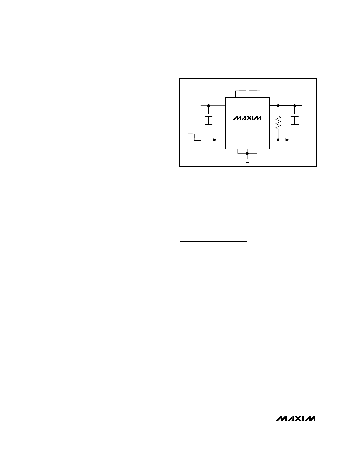
Figure 1. Typical Application Circuit
0.33µF
IN
+1.6V TO +5.5V
10µF
ON
OFF
CXN CXP
IN
MAX1759
SHDN
OUT
POK
PGNDGNDFB
OUT
3.3V AT 100mA
10µF
100k
POWER OK
Page 7

MAX1759
Buck/Boost Regulating
Charge Pump in µMAX
_______________________________________________________________________________________ 7
Figure 2. Functional Diagram
3, 4
PGND
SHDN
POK
CXN
78
IN
6
S1 S2
CXP
OUT
9
R1
MAX1759
BUCK-BOOST
CONTROL
2
1
BIAS
1.5MHz
OSC
ENABLE
1.235V
R2
FB
10
N
GND
5
OUT-LOW
1.1V
0.1V
Page 8

MAX1759
Buck/Boost Regulating
Charge Pump in µMAX
8 _______________________________________________________________________________________
Capacitor Selection
Optimize the charge-pump circuit for physical size, output current, and output ripple by selecting capacitors
CIN, CX, and C
OUT
. See Table 1 for suggested capacitor
values.
Note that capacitors must have low ESR (≤20mΩ) to
maintain low output ripple. Ceramic capacitors are
recommended. In cost-sensitive applications where high
output current is needed, the output capacitor may be a
combination of a 1µF ceramic in parallel with a 10µF tantalum capacitor. The ceramic capacitor’s low ESR will
help keep output ripple within acceptable levels.
Output Voltage Ripple
The MAX1759 proprietary control scheme automatically
chooses between voltage doubling and voltage stepdown to maintain output voltage regulation over various
load currents and VINto V
OUT
voltage differentials.
When VINis lower than V
OUT
, the charge pump always
operates in voltage-doubler mode. It regulates the output
voltage by modulating the charge delivered by the
transfer capacitor.
When VINis higher than V
OUT
, the charge pump operates in voltage step-down mode, but may revert to voltage-doubler mode if necessary to maintain regulation
under load. While operating in step-down mode, the
output voltage ripple is typically much lower than it is in
voltage-doubler mode (see Typical Operating
Characteristics).
Output Current
The MAX1759 is guaranteed to deliver a regulated 3.3V
at 100mA continuous, from a +2.5V input. Peaks up to
200mA are acceptable as long as the current is
≤100mA (RMS).
Applications Information
PC Board Layout
The MAX1759 is a high-frequency switched-capacitor
voltage regulator. For best circuit performance, use a
ground plane and keep CIN, CX, C
OUT
, and feedback
resistors (if used) close to the device. If using external
feedback, keep the feedback node as small as possible by positioning the feedback resistors very close to
FB. Suggested PC component placement and board
layout are shown in Figures 4a and 4b.
Chip Information
TRANSISTOR COUNT: 1802
Figure 3. Using External Feedback for Regulated 2.5V Output
Table 1. Capacitor Selection
OUTPUT
CURRENT
(mA)
100
100
50 2.2
4.7
10
C
IN
(µF)
CAPACITOR VALUE
OUTPUT RIPPLE
(mV)
C
X
(µF)
0.33
0.22
0.1 2.2
4.7
10
C
OUT
(µF)
VIN=
2.5V
40
80
100 80
60
20
VIN=
4.2V
0.33µF
CXN CXP
OUT
V
= 1.6V TO 5.5V
IN
10µF
IN
MAX1759
POK
SHDN
FB
PGNDGND
10µF
R1
76.8k
R2
75k
100k
= 2.5V
V
OUT
Page 9
MAX1759
Buck/Boost Regulating
Charge Pump in µMAX
_______________________________________________________________________________________ 9
Figure 4a. MAX1759 Component Placement Guide
Figure 4b. MAX1759 Recommended PC Board Layout
POK
SHDN
V
IN
R3 R2
C1
GND PLANE
R1
V
OUT
U1
C3
C2
POK
SHDN
V
V
IN
GND PLANE
OUT
Page 10

MAX1759
Buck/Boost Regulating
Charge Pump in µMAX
Package Information
Note: The MAX1759 does not have an exposed pad.
Maxim cannot assume responsibility for use of any circuitry other than circuitry entirely embodied in a Maxim product. No circuit patent licenses are
implied. Maxim reserves the right to change the circuitry and specifications without notice at any time.
10 ____________________Maxim Integrated Products, 120 San Gabriel Drive, Sunnyvale, CA 94086 408-737-7600
© 2000 Maxim Integrated Products Printed USA is a registered trademark of Maxim Integrated Products.
10LUMAX.EP
 Loading...