

Page 1
General Description
The MAX1748 triple-output DC-DC converter in a lowprofile TSSOP package provides the regulated voltages
required by active matrix, thin-film transistor (TFT) liquid
crystal displays (LCDs). One high-power DC-DC converter and two low-power charge pumps convert the
+3.3V to +5V input supply voltage into three independent
output voltages.
The primary high-power DC-DC converter generates a
boosted output voltage (V
MAIN
) up to 13V that is regulated within ±1%. The low-power BiCMOS control circuitry and the low on-resistance (0.35Ω) of the
integrated power MOSFET allows efficiency up to 93%.
The 1MHz current-mode PWM architecture provides
fast transient response and allows the use of ultra-small
inductors and ceramic capacitors.
The dual charge pumps independently regulate one
positive output (V
POS
) and one negative output (V
NEG
).
These low-power outputs use external diode and
capacitor stages (as many stages as required) to regulate output voltages up to +40V and down to -40V. A
proprietary regulation algorithm minimizes output ripple, as well as capacitor sizes for both charge pumps.
The MAX1748 is available in the ultra-thin TSSOP package (1.1mm max height).
________________________Applications
TFT Active Matrix LCD Displays
Passive Matrix LCD Displays
PDAs
Digital Still Cameras
Camcorders
Features
♦ Three Integrated DC-DC Converters
♦ 1MHz Current-Mode PWM Boost Regulator
Up to +13V Main High-Power Output
±1% Accuracy
High Efficiency (93%)
♦ Dual Charge-Pump Outputs
Up to +40V Positive Charge-Pump Output
Down to -40V Negative Charge-Pump Output
♦ Internal Supply Sequencing
♦ Internal Power MOSFETs
♦ +2.7V to +5.5V Input Supply
♦ 0.1µA Shutdown Current
♦ 0.6mA Quiescent Current
♦ Internal Soft-Start
♦ Power-Ready Output
♦ Ultra-Small External Components
♦ Thin TSSOP Package (1.1mm max)
MAX1748
Triple-Output TFT LCD DC-DC Converter
________________________________________________________________ Maxim Integrated Products 1
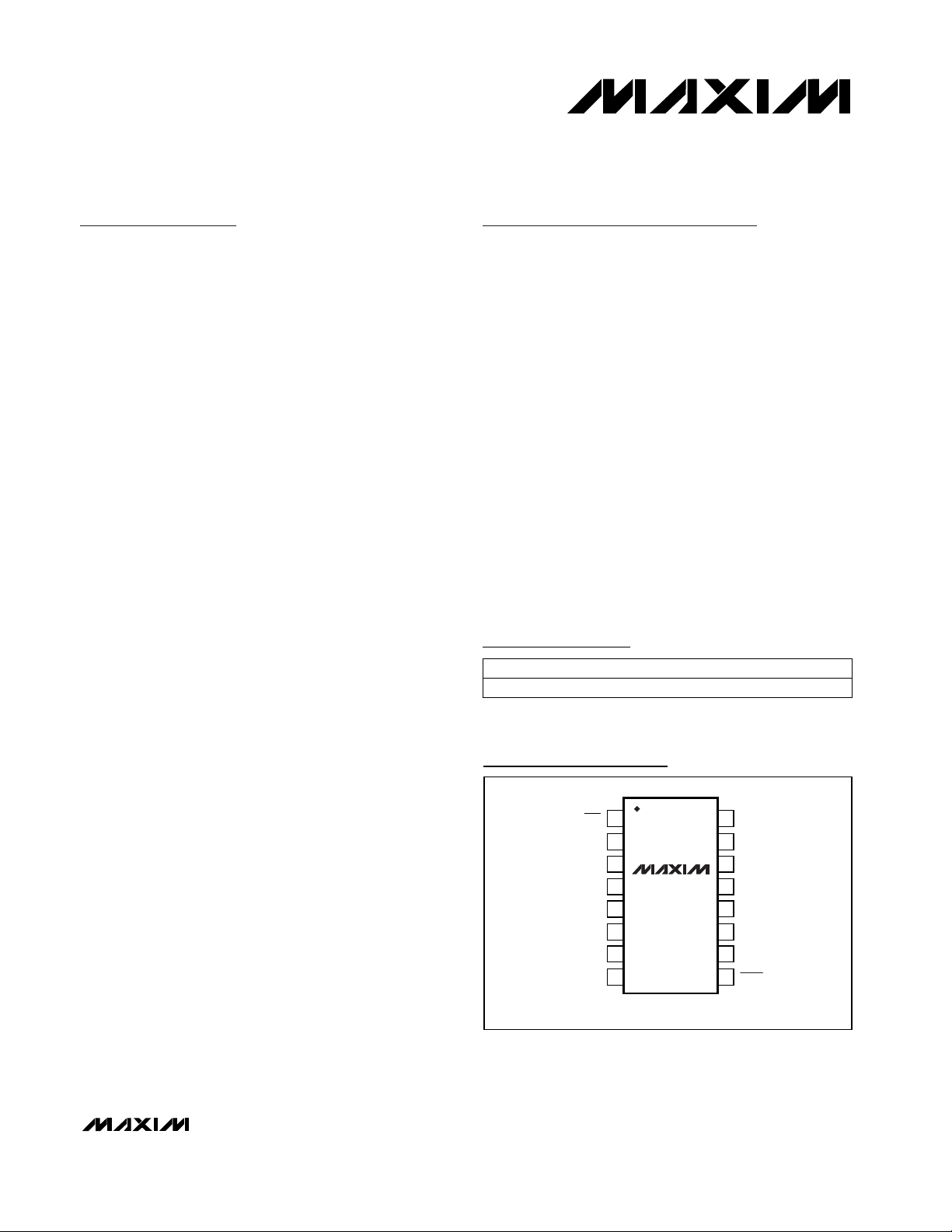
Pin Configuration
19-1740; Rev 0; 6/00
For free samples and the latest literature, visit www.maxim-ic.com or phone 1-800-998-8800.
For small orders, phone 1-800-835-8769.
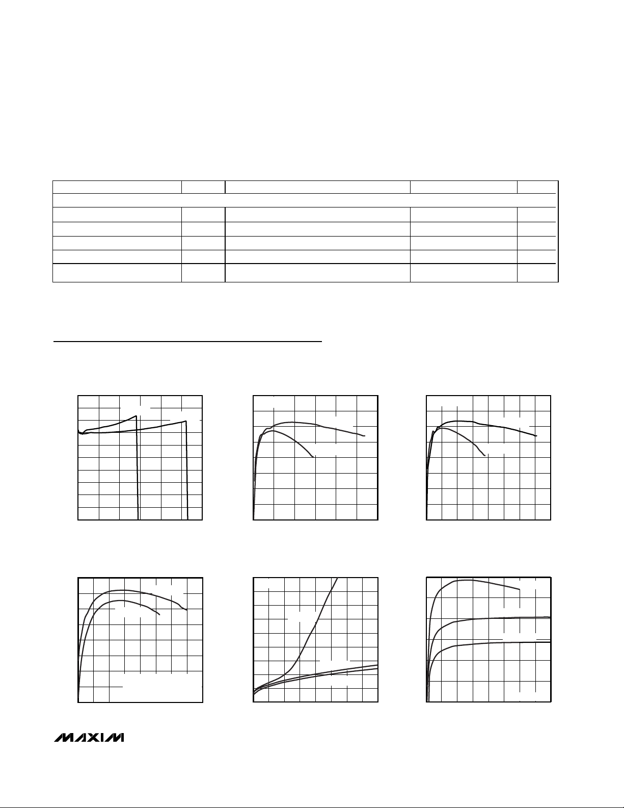
Ordering Information
Typical Operating Circuit appears at end of data sheet.
16 TSSOP
PIN-PACKAGETEMP. RANGE
-40°C to +85°CMAX1748EUE
PART
TOP VIEW
1
RDY TGND
FB
2
INTG
3
MAX1748
4
IN
GND
5
REF
6
FBP
7
FBN
8
TSSOP
16
15
LX
14
PGND
13
SUPP
12
DRVP
SUPN
11
10
DRVN
9
SHDN
Page 2
MAX1748
Triple-Output TFT LCD DC-DC Converter
2 _______________________________________________________________________________________
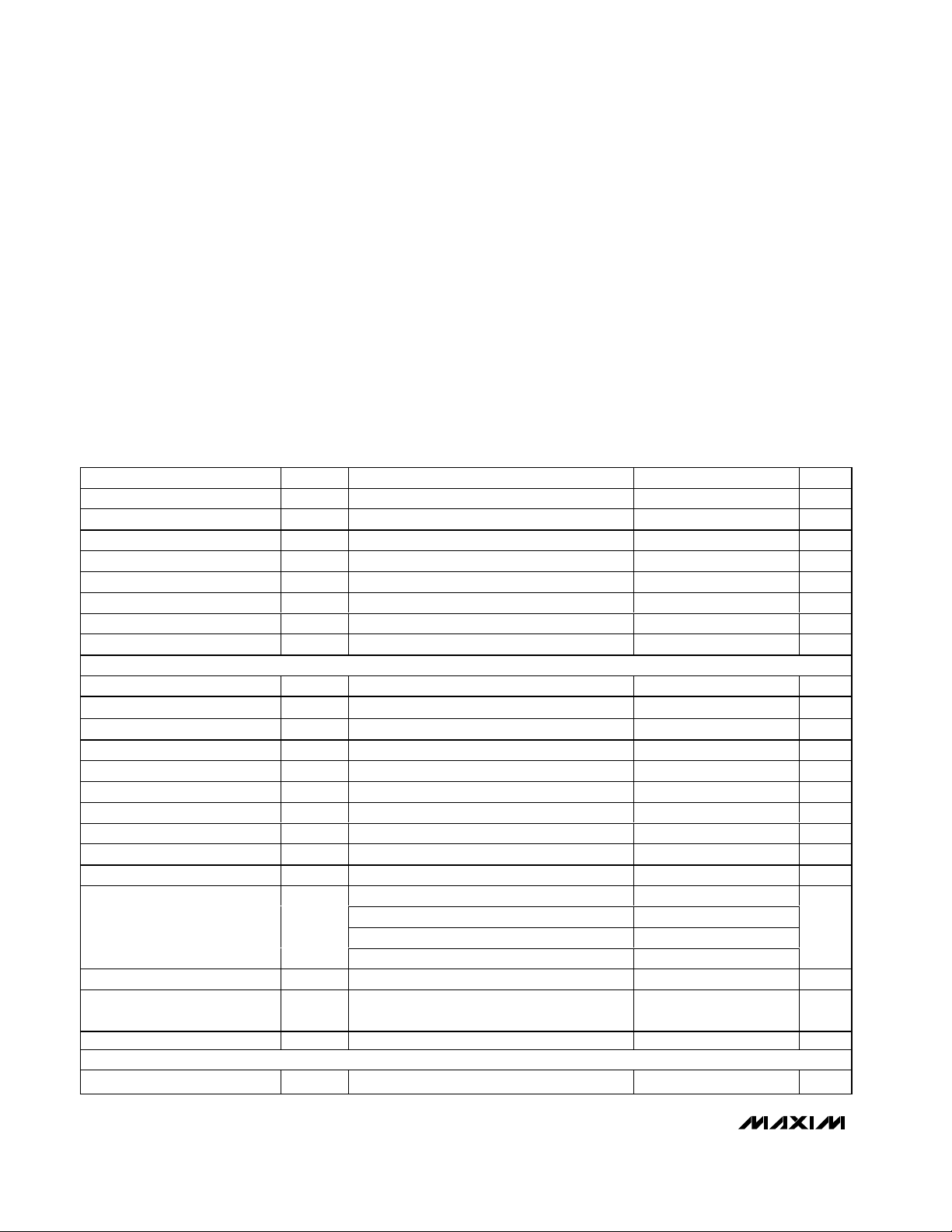
ABSOLUTE MAXIMUM RATINGS
ELECTRICAL CHARACTERISTICS
(VIN= +3.0V, SHDN = IN, V
SUPP
= V
SUPN
= 10V, TGND = PGND = GND, C
REF
= 0.22µF, C
INTG
= 470pF, TA= 0°C to +85°C, unless
otherwise noted. Typical values are at T
A
= +25°C.)
Stresses beyond those listed under “Absolute Maximum Ratings” may cause permanent damage to the device. These are stress ratings only, and functional
operation of the device at these or any other conditions beyond those indicated in the operational sections of the specifications is not implied. Exposure to
absolute maximum rating conditions for extended periods may affect device reliability.
IN, SHDN, TGND to GND .........................................-0.3V to +6V
DRVN to GND .........................................-0.3V to (V
SUPN
+ 0.3V)
DRVP to GND..........................................-0.3V to (V
SUPP
+ 0.3V)
PGND to GND.....................................................................±0.3V
RDY to GND ...........................................................-0.3V to +14V
LX, SUPP, SUPN to PGND .....................................-0.3V to +14V
INTG, REF, FB, FBN, FBP to GND...............-0.3V to (V
IN
+ 0.3V)
Continuous Power Dissipation (T
A
= +70°C)
16-Pin TSSOP (derate 9.4mW/°C above +70°C) ..........755mW
Operating Temperature Range
MAX1748EUE .................................................-40°C to +85°C
Junction Temperature......................................................+150°C
Storage Temperature Range .............................-65°C to +150°C
Lead Temperature (soldering, 10s) .................................+300°C
)
)
PARAMETER SYMBOL CONDITIONS MIN TYP MAX UNITS
Input Supply Range V
Input Undervoltage Threshold V
IN Quiescent Supply Current I
SUPP Quiescent Current I
SUPN Quiescent Current I
IN Shutdown Current V
SUPP Shutdown Current V
SUPN Shutdown Current V
MAIN BOOST CONVERTER
Output Voltage Range V
FB Regulation Voltage V
FB Input Bias Current I
Operating Frequency f
Oscillator Maximum Duty Cycle 78 85 90 %
Load Regulation I
Line Regulation 0.1 % / V
Integrator Gm 320 µmho
LX Switch On-Resistance R
LX Leakage Current I
LX Current Limit I
Maximum RMS LX Current 1A
Soft-Start Period t
FB Fault Trip Level 1.07 1.1 1.14 V
POSITIVE CHARGE PUMP
V
Input Supply Range V
SUPP
IN
UVLO
IN
SUPP
SUPN
MAIN
FB
FB
OSC
LX(ON
LX
VIN rising, 40mV hysteresis (typ) 2.2 2.4 2.6 V
VFB = V
V
FBP
V
FBN
SHDN
SHDN
SHDN
= 1.5V, V
FBP
= 1.5V 0.4 0.8 mA
= -0.1V 0.4 0.8 mA
= 0, V
IN
= 0, V
SUPP
= 0, V
SUPN
TA = 0°C to +85°C 1.235 1.248 1.261 V
VFB = 1.25V, INTG = GND -50 50 nA
= 0 to 200mA, V
MAIN
ILX = 100mA 0.35 0.7 Ω
VLX = 13V 0.01 20 µA
Phase I = soft-start (1.0ms) 0.275 0.380 0.500
Phase II = soft-start (1.0ms) 0.75
LX(MAX
Phase III = soft-start (1.0ms) 1.12
Phase IV = fully on (after 3.0ms) 1.1 1.5 2.0
SS
SUPP
Power-up to the end of Phase III
= -0.2V 0.6 1 mA
FBN
= 5V 0.1 10 µA
= 13V 0.1 10 µA
= 13V 0.1 10 µA
= 10V 0.2 %
MAIN
2.7 5.5 V
V
IN
13 V
0.85 1 1.15 MHz
A
3072 /
f
OSC
s
2.7 13 V
Page 3
MAX1748
Triple-Output TFT LCD DC-DC Converter
_______________________________________________________________________________________ 3
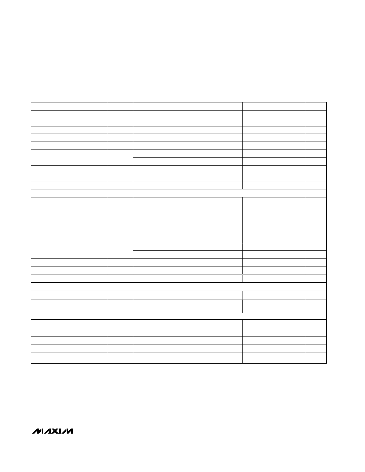
ELECTRICAL CHARACTERISTICS (continued)
(VIN= +3.0V, SHDN = IN, V
SUPP
= V
SUPN
= 10V, TGND = PGND = GND, C
REF
= 0.22µF, C
INTG
= 470pF, TA= 0°C to +85°C, unless
otherwise noted. Typical values are at T
A
= +25°C.)
PARAMETER SYMBOL CONDITIONS MIN TYP MAX UNITS
Operating Frequency
FBP Regulation Voltage V
FBP Input Bias Current I
DRVP PCH On-Resistance
DRVP NCH On-Resistance
FBP Power-Ready Trip Level Rising edge 1.091 1.125 1.159 V
FBP Fault Trip Level Falling edge 1.11 V
Maximum RMS DRVP Current 0.1 A
NEGATIVE CHARGE PUMP
V
Input Supply Range V
SUPN
Operating Frequency
FBN Regulation Voltage V
FBN Input Bias Current I
DRVN PCH On-Resistance
DRVN NCH On-Resistance
FBN Power-Ready Trip Level Rising edge 80 110 165 mV
FBN Fault Trip Level Falling edge 130 mV
Maximum RMS DRVN Current 0.1 A
REFERENCE
Reference Voltage V
Reference Undervoltage
Threshold
LOGIC SIGNALS
SHDN Input Low Voltage 0.4V hysteresis (typ) 0.9 V
SHDN Input High Voltage 2.1 V
SHDN Input Current I
RDY Output Low Voltage I
RDY Output High Voltage V
FBP
V
FBP
SUPN
FBN
FBN
REF
SHDN
= 1.5V -50 50 nA
FBP
V
= 1.213V 1.5 4 Ω
FBP
V
= 1.275V 20 kΩ
FBP
V
= -0.05V -50 50 nA
FBN
V
= 0.035V 1.5 4 Ω
FBN
= -0.025V 20 kΩ
V
FBN
-2µA < I
V
REF
SINK
RDY
< 50µA 1.231 1.25 1.269 V
REF
rising 0.9 1.05 1.2 V
= 2mA 0.25 0.5 V
= 13V 0.01 1 µA
0.5 ×
f
OSC
1.20 1.25 1.30 V
310Ω
2.7 13 V
0.5 ×
f
OSC
-50 0 50 mV
310Ω
0.01 1 µA
Hz
Hz
Page 4
MAX1748
Triple-Output TFT LCD DC-DC Converter
4 _______________________________________________________________________________________
)
)
ELECTRICAL CHARACTERISTICS (continued)
(VIN= +3.0V, SHDN = IN, V
SUPP
= V
SUPN
= 10V, TGND = PGND = GND, C
REF
= 0.22µF, C
INTG
= 470pF, TA= -40°C to +85°C,
unless otherwise noted.) (Note 1)
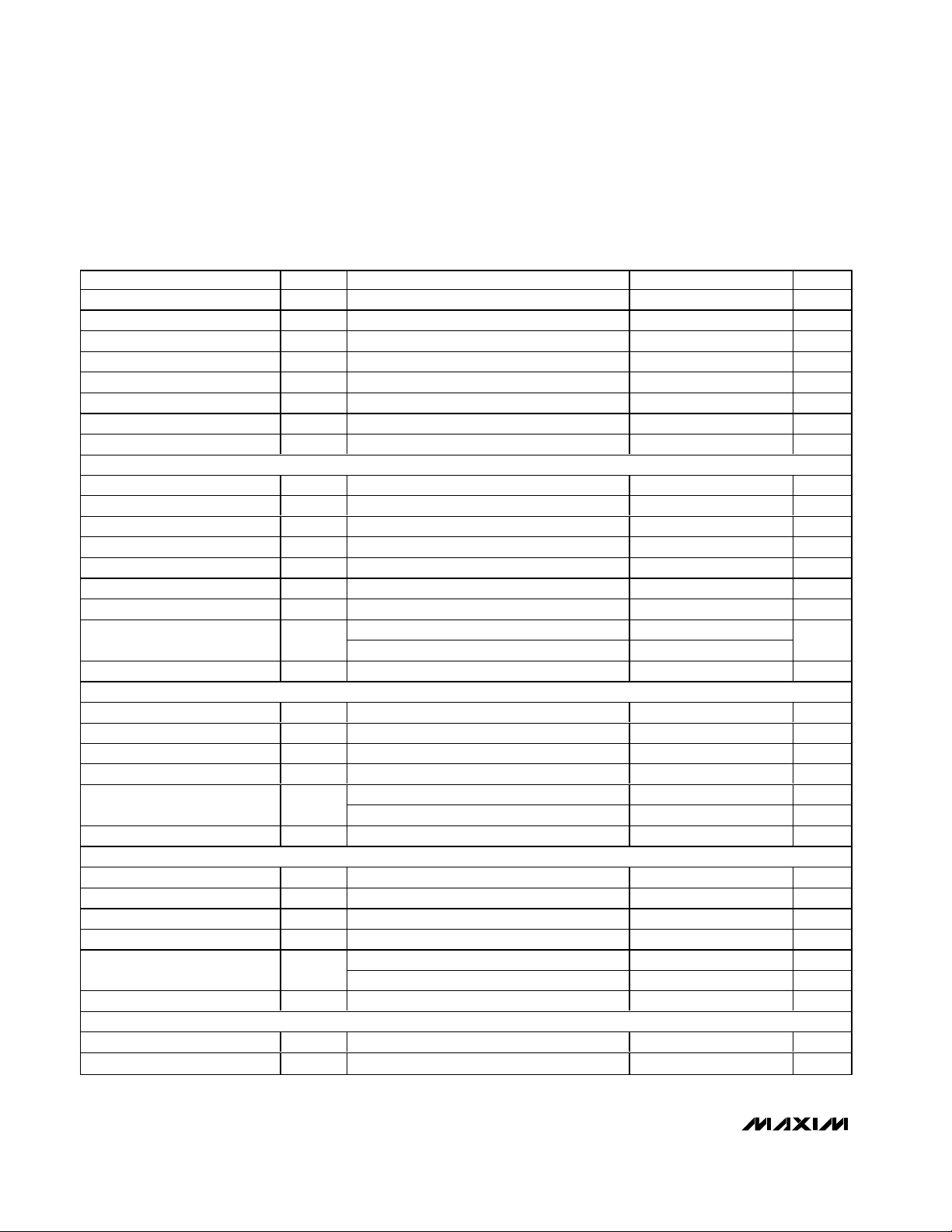
PARAMETER SYMBOL CONDITIONS MIN MAX UNITS
Input Supply Range V
Input Undervoltage Threshold V
IN Quiescent Supply Current I
SUPP Quiescent Current I
SUPN Quiescent Current I
IN Shutdown Current V
SUPP Shutdown Current V
SUPN Shutdown Current V
MAIN BOOST CONVERTER
Output Voltage Range V
FB Regulation Voltage V
FB Input Bias Current I
Operating Frequency F
Oscillator Maximum Duty Cycle 78 90 %
LX Switch On-Resistance R
LX Leakage Current
LX Current Limit I
FB Fault Trip Level 1.07 1.14 V
POSITIVE CHARGE PUMP
SUPP Input Supply Range V
FBP Regulation Voltage V
FBP Input Bias Current I
DRVP PCH On-Resistance 10 Ω
DRVP NCH On-Resistance
FBP Power-Ready Trip Level Rising edge 1.091 1.159 V
NEGATIVE CHARGE PUMP
SUPN Input Supply Range V
FBN Regulation Voltage V
FBN Input Bias Current
DRVN PCH On-Resistance
DRVN NCH On-Resistance
FBN Power-Ready Trip Level Rising edge 80 165 mV
REFERENCE
Reference Voltage V
Reference Undervoltage
LX(MAX
IN
UVLO
IN
SUPP
SUPN
MAIN
FB
OSC
LX(ON
I
LX
VIN rising, 40mV hysteresis (typ) 2.2 2.6 V
FB
VFB = V
V
FBP
V
FBN
SHDN
SHDN
SHDN
= 1.5V, V
FBP
= 1.5V 0.8 mA
= -0.1V 0.8 mA
= 0, VIN = 5V 10 µA
= 0, V
SUPP
= 0, V
SUPN
VFB = 1.25V, INTG = GND -50 50 nA
I
= 100mA 0.7 Ω
LX
VLX = 13V 20 µA
Phase I = soft-start (1.0ms) 0.275 0.500
Phase IV = fully on (after 3.0ms) 1.1 2.0
SUPP
FBP
V
FBP
SUPN
FBN
I
FBN
REF
= 1.5V -50 50 nA
FBP
V
= 1.213V 4 Ω
FBP
= 1.275V 20 kΩ
V
FBP
V
= -0.05V -50 50 nA
FBN
V
= 0.035V 4 Ω
FBN
= -0.025V 20 kΩ
V
FBN
-2µA < I
V
REF
< 50µA 1.223 1.269 V
REF
rising 0.9 1.2 V
2.7 5.5 V
= -0.2V 1 mA
FBN
= 13V 10 µA
= 13V 10 µA
V
IN
1.225 1.271 V
0.75 1.25 MHz
2.7 13 V
1.20 1.30 V
2.7 13 V
-50 50 mV
13 V
A
10 Ω
Page 5
MAX1748
Triple-Output TFT LCD DC-DC Converter
_______________________________________________________________________________________ 5
V
(V)
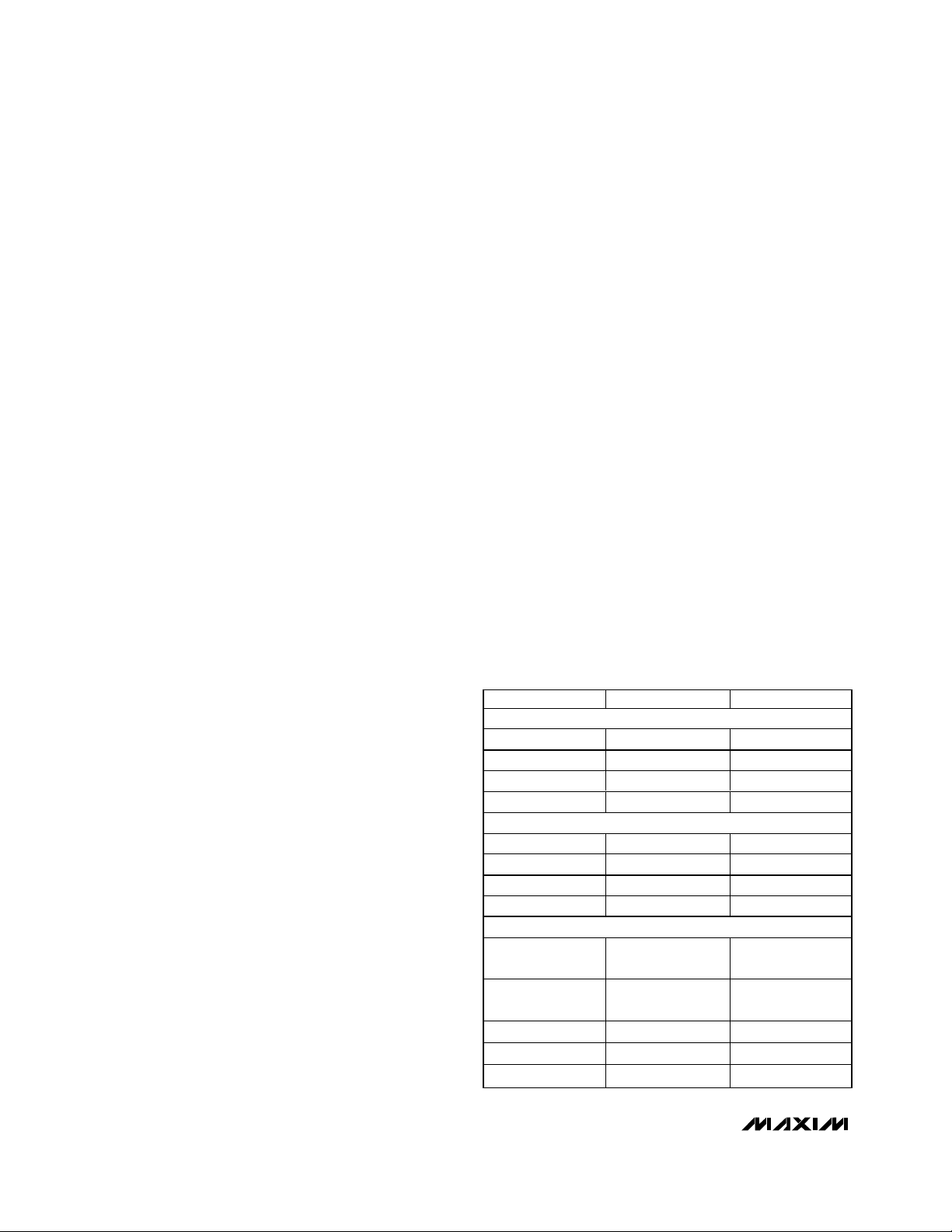
Typical Operating Characteristics
(Circuit of Figure 5, VIN= 3.3V, TA= +25°C, unless otherwise noted.)
ELECTRICAL CHARACTERISTICS (continued)
(VIN= +3.0V, SHDN = IN, V
SUPP
= V
SUPN
= 10V, TGND = PGND = GND, C
REF
= 0.22µF, C
INTG
= 470pF, TA= -40°C to +85°C,
unless otherwise noted.) (Note 1)
Note 1: Specifications from 0°C to -40°C are guaranteed by design, not production tested.
PARAMETER SYMBOL CONDITIONS MIN MAX UNITS
LOGIC SIGNALS
SHDN Input Low Voltage 0.45V hysteresis (typ) 0.9 V
SHDN Input High Voltage 2.1 V
Input Current I
SHDN
RDY Output Low Voltage I
RDY Output High Leakage V
SHDN
= 2mA 0.5 V
SINK
= 13V 1 µA
RDY
1 µA
MAIN OUTPUT VOLTAGE
vs. LOAD CURRENT
10.04
10.02
10.00
9.98
9.96
(V)
9.94
MAIN
V
9.92
9.90
9.88
9.86
9.84
0 200100 300 400 500 600
VIN = 3.3V
I
(mA)
MAIN
VIN = 5.0V
100
MAX1748 toc01
EFFICIENCY (%)
MAIN STEP-UP CONVERTER
EFFICIENCY vs. LOAD CURRENT
(BOOST ONLY)
V
= 10V
MAIN
95
90
85
80
75
70
65
60
0 200100 300 400 500 600
VIN = 3.3V
I
MAIN
(mA)
VIN = 5.0V
100
MAX1748toc02
EFFICIENCY (%)
MAIN STEP-UP CONVERTER
EFFICIENCY vs. LOAD CURRENT
(BOOST ONLY)
V
= 8V
MAIN
95
VIN = 3.3V
I
MAIN
VIN = 5.0V
(mA)
90
85
80
75
70
65
60
0 200100 300 400 500 800600 700
MAX1748toc03
EFFICIENCY vs. LOAD CURRENT
(BOOST CONVERTER AND CHARGE PUMPS)
90
V
= 8V
= 10V
= -5V WITH I
NEG
= 15V WITH I
POS
I
(mA)
MAIN
MAIN
NEG
POS
= 10mA
= 5mA
MAX1748toc04
85
80
75
70
65
EFFICIENCY (%)
60
55
50
0 10050 150 200 250 400300 350
V
MAIN
VIN = 3.3V
V
V
NEGATIVE CHARGE-PUMP OUTPUT
VOLTAGE vs. LOAD CURRENT
-4.60
V
= -5V
NEG
-4.65
-4.70
V
= 6V
-4.75
-4.80
NEG
-4.85
-4.90
-4.95
-5.00
-5.05
015205 10 25303540
SUPN
V
= 8V
SUPN
V
= 10V
SUPN
I
(mA)
NEG
MAX1748toc05
NEGATIVE CHARGE-PUMP EFFICIENCY
vs. LOAD CURRENT
80
70
60
50
EFFICIENCY (%)
40
30
20
015205 10 25303540
I
NEG
(mA)
V
V
SUPN
SUPN
V
= 8V
= 10V
SUPN
V
NEG
= 6V
MAX1748toc06
= -5V
Page 6

MAX1748
Triple-Output TFT LCD DC-DC Converter
6 _______________________________________________________________________________________
Typical Operating Characteristics (continued)
(Circuit of Figure 5, VIN= 3.3V, TA= +25°C, unless otherwise noted.)
8
10
18
20
12
16
14
22
24
58796101112
MAXIMUM POSITIVE CHARGE-PUMP OUTPUT
VOLTAGE vs. SUPPLY VOLTAGE
MAX1748toc10
V
SUPP
(V)
V
POS
(V)
I
POS
= 10mA
V
POS
= 22V
I
POS
= 1mA
I
POS
= 20mA
0.80
0.85
0.90
1.05
1.00
0.95
1.10
1.15
1.20
2.5 3.53.0 4.0 4.5 5.0 5.5
SWITCHING FREQUENCY
vs. INPUT VOLTAGE
MAX1748toc11
INPUT VOLTAGE (V)
SWITCHING FREQUENCY (MHz)
MEASURED FROM THE
FALLING EDGE OF LX
V
MAIN
= 10V
I
MAIN
= 100mA
1.244
1.246
1.250
1.248
1.252
1.254
0201510 3025535404550
REFERENCE VOLTAGE
vs. REFERENCE LOAD CURRENT
MAX1748toc12
I
REF
(µA)
V
REF
(V)
VIN = 3.3V
V
MAIN
10mV/div
V
NEG
10mV/div
V
POS
10mV/div
RIPPLE WAVEFORMS
MAX1748toc13
1µs/div
V
MAIN
= 10V, I
MAIN
= 200mA,
V
NEG
= -5V, I
NEG
= 10mA,
V
POS
= 15V, I
POS
= 10mA
I
MAIN
200mA/div
I
LX
500mA/div
V
MAIN
200mV/div
LOAD-TRANSIENT RESPONSE
MAX1748 toc14
100µs/div
V
IN
= 3.3V, V
MAIN
= 10V,
R
MAIN
= 500Ω TO 50Ω (20mA TO 200mA)
I
MAIN
200mA/div
I
LX
500mA/div
V
MAIN
200mV/div
LOAD-TRANSIENT RESPONSE
WITHOUT INTEGRATOR
MAX1748toc15
100µs/div
V
IN
= 3.3V, V
MAIN
= 10V, INTG = REF,
R
MAIN
= 500Ω TO 50Ω (20mA TO 200mA)
-11
-9
-10
-7
-8
-4
-5
-6
-3
5867 9101112
MAXIMUM NEGATIVE CHARGE-PUMP
OUTPUT VOLTAGE vs. SUPPLY VOLTAGE
MAX1748toc07
V
SUPN
(V)
V
NEG
(V)
I
NEG
= 20mA
I
NEG
= 1mA
I
NEG
= 10mA
V
NEG
= -10mA
14.4
14.5
14.6
14.9
15.0
14.7
14.8
15.2
15.1
15.3
086102 4 12 14 16 18 20
POSITIVE CHARGE-PUMP OUTPUT
VOLTAGE vs. LOAD CURRENT
MAX1748toc08
I
POS
(mA)
V
POS
(V)
V
SUPN
= 12V
V
SUPN
= 8V
V
SUPN
= 10V
40
50
80
60
70
90
100
086102 4 12 14 16 18 20
POSITIVE CHARGE-PUMP EFFICIENCY
vs. LOAD CURRENT
MAX1748toc09
I
POS
(mA)
EFFICIENCY (%)
V
SUPP
= 12V
V
SUPP
= 8V
V
SUPP
= 10V
Page 7

MAX1748
Triple-Output TFT LCD DC-DC Converter
_______________________________________________________________________________________ 7
Typical Operating Characteristics (continued)
(Circuit of Figure 5, VIN= 3.3V, TA= +25°C, unless otherwise noted.)
Pin Description
V
MAIN
5V/div
2V
10V
0
I
LX
500mA/div
MAIN BOOST STARTUP WAVEFORM
MAX1748toc16
1ms/div
R
MAIN
= 1kΩ, V
MAIN
= 10V
V
SHDN
2V/div
0
0
V
MAIN
5V/div
2V
10V
0
I
LX
500mA/div
MAIN BOOST STARTUP
WAVEFORM WITH LOAD
MAX1748toc17
1ms/div
V
MAIN
= 10V, R
MAIN
= 50Ω (200mA)
V
SHDN
2V/div
0
0
V
MAIN
5V/div
V
NEG
5V/div
V
POS
10V/div
POWER-UP SEQUENCING
MAX1748toc18
2ms/div
V
MAIN
= 10V, V
NEG
= -5V, V
POS
= 15V
V
SHDN
2V/div
PIN NAME FUNCTION
1 RDY Active-Low Open-Drain Output. Indicates all outputs are ready. The on-resistance is 125Ω (typ).
2FB
3 INTG
4IN
5 GND Analog Ground. Connect to power ground (PGND) underneath the IC.
6 REF
7 FBP
8 FBN Negative Charge-Pump Regulator Feedback Input. Regulates to 0V nominal.
9
10 DRVN Negative Charge-Pump Driver Output. Output high level is V
11 SUPN Negative Charge-Pump Driver Supply Voltage. Bypass to PGND with a 0.1µF capacitor.
12 DRVP Positive Charge-Pump Driver Output. Output high level is V
Main Boost Regulator Feedback Input. Regulates to 1.248V nominal. Connect feedback resistive
divider to analog ground (GND).
Main Boost Integrator Output. If used, connect 470pF to analog ground (GND). To disable
integrator, connect to REF.
Supply Input. +2.7V to +5.5V input range. Bypass with a 0.1µF capacitor between IN and GND, as
close to the pins as possible.
Internal Reference Bypass Terminal. Connect a 0.22µF capacitor from this terminal to analog
ground (GND). External load capability to 50µA.
Positive Charge-Pump Regulator Feedback Input. Regulates to 1.25V nominal. Connect feedback
resistive divider to analog ground (GND).
SHDN
Active-Low Logic-Level Shutdown Input. Connect SHDN to IN for normal operation.
, and low level is PGND.
SUPN
, and low level is PGND.
SUPP
Page 8

MAX1748
Triple-Output TFT LCD DC-DC Converter
8 _______________________________________________________________________________________
Detailed Description
The MAX1748 is a highly efficient triple-output power
supply for TFT LCD applications. The device contains
one high-power step-up converter and two low-power
charge pumps. The primary boost converter uses an
internal N-channel MOSFET to provide maximum efficiency and to minimize the number of external components. The output voltage of the main boost converter
(V
MAIN
) can be set from VINto 13V with external resistors.
The dual charge pumps independently regulate a positive output (V
POS
) and a negative output (V
NEG
). These
low-power outputs use external diode and capacitor
stages (as many stages as required) to regulate output
voltages up to +40V and down to -40V. A proprietary
regulation algorithm minimizes output ripple as well as
capacitor sizes for both charge pumps.
Also included in the MAX1748 are a precision 1.25V
reference that sources up to 50µA, logic shutdown,
soft-start, power-up sequencing, fault detection, and an
active-low open-drain ready output.
Main Boost Converter
The MAX1748 main step-up converter switches at a
constant 1MHz internal oscillator frequency to allow the
use of small inductors and output capacitors. The
MOSFET switch pulse width is modulated to control the
power transferred on each switching cycle and to regulate the output voltage.
During PWM operation, the internal clock’s rising edge
sets a flip-flop, which turns on the N-channel MOSFET
(Figure 1). The switch turns off when the sum of the
voltage-error, slope-compensation, and current-feedback signals trips the multi-input comparator and
resets the flip-flop. The switch remains off for the rest of
the clock cycle. Changes in the output voltage error
signal shift the switch current trip level, consequently
modulating the MOSFET duty cycle.
Dual Charge-Pump Regulator
The MAX1748 contains two individual low-power charge
pumps. One charge pump inverts the supply voltage
(SUPN) and provides a regulated negative output voltage.
The second charge pump doubles the supply voltage
(SUPP) and provides a regulated positive output voltage.
The MAX1748 contains internal P-channel and N-channel
MOSFETs to control the power transfer. The internal
MOSFETs switch at a constant 500kHz (0.5 ✕f
OSC
).
Negative Charge Pump
During the first half-cycle, the P-channel MOSFET turns
on and the flying capacitor C5 charges to V
SUPN
minus
a diode drop (Figure 2). During the second half-cycle,
the P-channel MOSFET turns off, and the N-channel
MOSFET turns on, level shifting C5. This connects C5 in
parallel with the reservoir capacitor C6. If the voltage
across C6 minus a diode drop is lower than the voltage
across C5, charge flows from C5 to C6 until the diode
(D5) turns off. The amount of charge transferred to the
output is controlled by the variable N-channel on-resistance.
Positive Charge Pump
During the first half-cycle, the N-channel MOSFET turns
on and charges the flying capacitor C3 (Figure 3). This
initial charge is controlled by the variable N-channel
on-resistance. During the second half-cycle, the Nchannel MOSFET turns off and the P-channel MOSFET
turns on, level shifting C3 by V
SUPP
volts. This connects
C3 in parallel with the reservoir capacitor C4. If the voltage across C4 plus a diode drop (V
POS
+ V
DIODE
) is
smaller than the level-shifted flying capacitor voltage
(VC3+ V
SUPP
), charge flows from C3 to C4 until the
diode (D3) turns off.
Soft-Start
For the main boost regulator, soft-start allows a gradual
increase of the internal current-limit level during startup
to reduce input surge currents. The MAX1748 divides
Pin Description (continued)
PIN NAME FUNCTION
13 SUPP Positive Charge-Pump Driver Supply Voltage. Bypass to PGND with a 0.1µF capacitor.
14 PGND Power Ground. Connect to GND underneath the IC.
15 LX
16 TGND Must be connected to ground.
Main Boost Regulator Power MOSFET N-Channel Drain. Connect output diode and output capacitor
as close to PGND as possible.
Page 9

MAX1748
Triple-Output TFT LCD DC-DC Converter
_______________________________________________________________________________________ 9
the soft-start period into four phases. During phase 1,
the MAX1748 limits the current limit to only 0.38A (see
Electrical Characteristics), approximately a quarter of
the maximum current limit (I
LX(MAX)
). If the output does
not reach regulation within 1ms, soft-start enters phase
II and the current limit is increased by another 25%.
This process is repeated for phase III. The maximum
1.5A (typ) current limit is reached within 3.0ms or when
the output reaches regulation, whichever occurs first
(see the Startup Waveforms in the Typical Operating
Characteristics).
For the charge pumps, soft-start is achieved by controlling the rise rate of the output voltage. The output voltage regulates within 4ms, regardless of output
capacitance and load, limited only by the regulator’s
output impedance.
Shutdown
A logic-low level on SHDN disables all three MAX1748
converters and the reference. When shut down, supply
current drops to 0.1µA to maximize battery life and the
reference is pulled to ground. The output capacitance
and load current determine the rate at which each output voltage will decay. A logic-level high on SHDN
power activates the MAX1748 (see Power-Up
Sequencing). Do not leave SHDN floating. If unused,
connect SHDN to IN.
Power-Up Sequencing
Upon power-up or exiting shutdown, the MAX1748
starts a power-up sequence. First, the reference powers up. Then the main DC-DC step-up converter powers up with soft-start enabled. Once the main boost
Figure 1. PWM Boost Converter Block Diagram
OSC
= 2.7V TO 5.5V
V
IN
IN
S
R
+
Q
I
LIM
L1
LX
PGND
D1
V
[1 + (R1 / R2)] x V
OUT =
V
= 1.25V
REF
R1
V
MAIN
(UP TO 13V)
C1
REF
+
R
+
-
INTG
C
INTG
MAX1748
Gm
+
+
-
-
1.25V
FB
REF
GND
C2
COMP
R2
C
COMP
Page 10

MAX1748
Triple-Output TFT LCD DC-DC Converter
10 ______________________________________________________________________________________
Figure 2. Negative Charge-Pump Block Diagram
Figure 3. Positive Charge-Pump Block Diagram
= 2.7V TO 13V
V
SUPN
D4
D5
OSC
SUPN
DRVN
C5
+
-
MAX1748
GND
OSC
R6
C
REF
0.22µF
R5
V
= (R5 / R6) x V
POS
V
= 1.25V
REF
V
SUPP
D2
D3
FBN
V
-
REF
+
1.25V
PGND
REF
SUPP
DRVP
C3
V
C6
= 2.7V TO 13V
NEG
REF
-
FBP
+
+
V
REF
-
1.25V
R3
R4
V
POS
C4
MAX1748
GND
PGND
V
= [1 + (R3 / R4)] x V
POS
V
= 1.25V
REF
REF
Page 11

MAX1748
Triple-Output TFT LCD DC-DC Converter
______________________________________________________________________________________ 11
converter reaches regulation, the negative charge
pump turns on. When the negative output voltage
reaches approximately 88% of its nominal value (V
FBN
< 110mV), the positive charge pump starts up. Finally,
when the positive output voltage reaches 90% of its
nominal value (V
FBP
> 1.125V), the active-low ready
signal (RDY) goes low (see Power Ready section).
Power Ready
Power ready is an open-drain output. When the powerup sequence is properly completed, the MOSFET turns
on and pulls RDY low with a typical 125Ω on-resistance. If a fault is detected, the internal open-drain
MOSFET appears as a high impedance. Connect a
100kΩ pull-up resistor between RDY and IN for a logiclevel output.
Fault Detection
Once RDY is low and if any output falls below its faultdetection threshold, RDY goes high impedance.
For the reference, the fault threshold is 1.05V. For the
main boost converter, the fault threshold is 88% of its
nominal value (VFB< 1.1V). For the negative charge
pump, the fault threshold is approximately 90% of its
nominal value (V
FBN
< 130mV). For the positive charge
pump, the fault threshold is 88% of its nominal value
(V
FBP
< 1.11V).
Once an output faults, all outputs later in the power
sequence shut down until the faulted output rises
above its power-up threshold. For example, if the negative charge-pump output voltage falls below the fault
detection threshold, the main boost converter remains
active while the positive charge pump stops switching
and its output voltage decays, depending on output
capacitance and load. The positive charge-pump output will not power up until the negative charge-pump
output voltage rises above its power-up threshold (see
the Power-Up Sequencing section).
Voltage Reference
The voltage at REF is nominally 1.25V. The reference
can source up to 50µA with good load regulation (see
Typical Operating Characteristics). Connect a 0.22µF
bypass capacitor between REF and GND.
Design Procedure
Main Boost Converter
Output Voltage Selection
Adjust the output voltage by connecting a voltage
divider from the output (V
MAIN
) to FB to GND (see
Typical Operating Circuit). Select R2 in the 10kΩ to
20kΩ range. Higher resistor values improve efficiency
at low output current but increase output voltage error
due to the feedback input bias current. Calculate R1
with the following equations:
R1 = R2 [(V
MAIN
/ V
REF
) - 1]
where V
REF
= 1.25V. V
MAIN
may range from VINto 13V.
Feedback Compensation
For stability, add a pole-zero pair from FB to GND in the
form of a series resistor (R
COMP
) and capacitor
(C
COMP
). The resistor should be half the value of the
R2 feedback resistor.
Inductor Selection
Inductor selection depends on input voltage, output
voltage, maximum current, switching frequency, size,
and availability of inductor values. Other factors can
include efficiency and ripple voltage. Inductors are
specified by their inductance (L), peak current (I
PEAK
),
and resistance (RL). The following boost-circuit equations are useful in choosing inductor values based on
the application. They allow the trading of peak current
and inductor value while allowing for consideration of
component availability and cost.
The following equation includes a constant LIR, which
is the ratio of the inductor peak-to-peak AC current to
maximum average DC inductor current. A good compromise between the size of the inductor, loss, and output ripple is to choose an LIR of 0.3 to 0.5. The peak
inductor current is then given by:
The inductance value is then given by:
Considering the typical application circuit, the maximum DC load current (I
MAIN(MAX)
) is 200mA with a 10V
output. A 6.8µH inductance value is then chosen,
based on the above equations and using 85% efficiency and a 1MHz operating frequency. Smaller inductance values typically offer a smaller physical size for a
given series resistance and current rating, allowing the
smallest overall circuit dimensions. However, due to
higher peak inductor currents, the output voltage ripple
(I
PEAK
✕
output filter capacitor ESR) will be higher.
Use inductors with a ferrite core or equivalent; powder
iron cores are not recommended for use with the
MAX1748’s high switching frequencies. The inductor’s
maximum current rating should exceed I
PEAK
. Under
fault conditions, inductor current may reach up to 2.0A.
I
PEAK
L
=
IV
MAIN(MAX) MAIN
=
Efficiency V
2
V Efficiency (V V )
IN(MIN)
××−
V LIR I f
(MAIN)
×
×
IN(MIN)
2
×× ×
MAIN(MAX) OSC
1 (LIR/2)
×+
[]
MAIN IN(MIN)
Page 12
MAX1748
Triple-Output TFT LCD DC-DC Converter
The MAX1748’s fast current-limit circuitry allows the use
of soft-saturation inductors while still protecting the IC.
The inductor’s DC resistance significantly affects efficiency. For best performance, select inductors with
resistance less than the internal N-channel FET resistance. To minimize radiated noise in sensitive applications, use a shielded inductor.
The inductor should have as low a series resistance as
possible. For continuous inductor current, the power
loss in the inductor resistance, PLR, is approximated by:
P
LR
≅ (I
MAIN
✕
V
MAIN
/ VIN)
2
✕
R
L
where RLis the inductor series resistance.
Output Capacitor
A 10µF capacitor works well in most applications. The
equivalent series resistance (ESR) of the output filter
capacitor affects efficiency and output ripple. Output
voltage ripple is largely the product of the peak inductor current and the output capacitor ESR. Use low-ESR
ceramic capacitors for best performance. Low-ESR,
surface-mount tantalum capacitors with higher capacity
may be used for load transients with high peak currents. Voltage ratings and temperature characteristics
should be considered.
Input Capacitor
The input capacitor (CIN) in boost designs reduces the
current peaks drawn from the input supply and reduces
noise injection. The value of CINis largely determined
by the source impedance of the input supply. High
source impedance requires high input capacitance,
particularly as the input voltage falls. Since step-up DCDC converters act as “constant-power” loads to their
input supply, input current rises as input voltage falls. A
good starting point is to use the same capacitance
value for CINas for C
OUT
. Table 1 lists suggested com-
ponent suppliers.
Integrator Capacitor
The MAX1748 contains an internal current integrator
that improves the DC load regulation but increases the
peak-to-peak transient voltage (see the load-transient
waveforms in the Typical Operating Characteristics).
For highly accurate DC load regulation, enable the current integrator by connecting a 470pF capacitor to
INTG. To minimize the peak-to-peak transient voltage at
the expense of DC regulation, disable the integrator by
connecting INTG to REF and adding a 100kΩ resistor
to GND.
Rectifier Diode
Use a Schottky diode with an average current rating
equal to or greater than the peak inductor current, and
a voltage rating at least 1.5 times the main output voltage (V
MAIN
).
Charge Pump
Efficiency Considerations
The efficiency characteristics of the MAX1748 regulated
charge pumps are similar to a linear regulator. They are
dominated by quiescent current at low output currents
and by the input voltage at higher output currents (see
Typical Operating Characteristics). So the maximum
efficiency may be approximated by:
Efficiency ≅ V
NEG
/ [V
IN
✕
N];
for the negative charge pump
Efficiency ≅ V
POS
/ [V
IN
✕
(N + 1)];
for the positive charge pump
where N is the number of charge-pump stages.
Output Voltage Selection
Adjust the positive output voltage by connecting a voltage-divider from the output (V
POS
) to FBP to GND (see
Typical Operating Circuit). Adjust the negative output
Table 1. Component Suppliers
12 ______________________________________________________________________________________
SUPPLIER PHONE FAX
INDUCTORS
Coilcraft 847-639-6400 847-639-1469
Coiltronics 561-241-7876 561-241-9339
Sumida USA 847-956-0666 847-956-0702
Toko 847-297-0070 847-699-1194
CAPACITORS
AVX 803-946-0690 803-626-3123
Kemet 408-986-0424 408-986-1442
Sanyo 619-661-6835 619-661-1055
Taiyo Yuden 408-573-4150 408-573-4159
DIODES
Central
Semiconductor
International
Rectifier
Motorola 602-303-5454 602-994-6430
Nihon 847-843-7500 847-843-2798
Zetex 516-543-7100 516-864-7630
516-435-1110 516-435-1824
310-322-3331 310-322-3332
Page 13

MAX1748
Triple-Output TFT LCD DC-DC Converter
______________________________________________________________________________________ 13
voltage by connecting a voltage-divider from the output
(V
NEG
) to FBN to REF. Select R4 and R6 in the 50kΩ to
100kΩ range. Higher resistor values improve efficiency
at low output current but increase output voltage error
due to the feedback input bias current. Calculate the
remaining resistors with the following equations:
R3 = R4 [(V
POS
/ V
REF
) - 1]
R5 = R6 (V
NEG
/ V
REF
)
where V
REF
= 1.25V. V
POS
may range from V
SUPP
to
40V, and V
NEG
may range from 0 to -40V.
Flying Capacitor
Increasing the flying capacitor’s value reduces the output current capability. Above a certain point, increasing
the capacitance has a negligible effect because the
output current capability becomes dominated by the
internal switch resistance and the diode impedance.
Start with 0.1µF ceramic capacitors. Smaller values
may be used for low-current applications.
Charge-Pump Output Capacitor
Increasing the output capacitance or decreasing the
ESR reduces the output ripple voltage and the peak-topeak transient voltage. Use the following equation to
approximate the required capacitor value:
C
OUT
≥ [I
OUT
/ (500kHz ✕V
RIPPLE
)]
Charge-Pump Input Capacitor
Use a bypass capacitor with a value equal to or greater
than the flying capacitor. Place the capacitor as close
to the IC as possible. Connect directly to PGND.
Rectifier Diode
Use Schottky diodes with a current rating equal to or
greater than 4 times the average output current, and a
voltage rating at least 1.5 times V
SUPP
for the positive
charge pump and V
SUPN
for the negative charge pump.
PC Board Layout and Grounding
Careful printed circuit layout is extremely important to
minimize ground bounce and noise. First, place the
main boost converter output diode and output capacitor
less than 0.2in (5mm) from the LX and PGND pins with
wide traces and no vias. Then place 0.1µF ceramic
bypass capacitors near the charge-pump input pins
(SUPP and SUPN) to the PGND pin. Keep the chargepump circuitry as close to the IC as possible, using
wide traces and avoiding vias when possible. Locate all
feedback resistive dividers as close to their respective
feedback pins as possible. The PC board should feature separate GND and PGND areas connected at only
one point under the IC. To maximize output power and
efficiency and to minimize output power ripple voltage,
use extra wide power ground traces and solder the IC’s
power ground pin directly to it. Avoid having sensitive
traces near the switching nodes and high-current lines.
Refer to the MAX1748 evaluation kit for an example of
proper board layout.
Applications Information
Boost Converter Using a
Cascoded MOSFET
For applications that require output voltages greater
than 13V, cascode an external N-channel MOSFET
(Figure 4). Place the MOSFET as close to the LX pin as
possible. Connect the gate to the input voltage (V
IN
)
and the source to LX.
MOSFET Selection
Choose a MOSFET with an on-resistance (R
DS(ON)
)
lower than the internal N-channel MOSFET. Lower
R
DS(ON)
will improve efficiency. The external N-channel
MOSFET must have a drain-voltage rating higher than
the main output voltage (V
MAIN
).
Chip Information
TRANSISTOR COUNT: 2846
Page 14

MAX1748
Triple-Output TFT LCD DC-DC Converter
14 ______________________________________________________________________________________
Figure 4. Power Supply Using Cascoded MOSFET
+25V, 5mA
=
V
POS
1.0µF
OUT
= +18V, 140mA
C
MAIN
V
0.47µF
10µF
COMP
C
68nF
6.8µH
R1
100k
130k
COMP
R
R2
5k
IN SUPP
10k
SUPN
R3
1M
R4
49.9k
INTG
C
470pF
0.22µF
LX
FB
DRVP
0.1µF
FBP
INTG
TGND
GND
MAX1748
SHDN
RDY
DRVN
0.22µF
0.1µF
FBN
REF
PGND
R6
49.9k
R5
319k
REF
C
0.22µF
3.3µF
1.0µF
= 5.0V
IN
V
0.47µF
= -8V, 20mA
NEG
V
Page 15

MAX1748
Triple-Output TFT LCD DC-DC Converter
______________________________________________________________________________________ 15
Typical Operating Circuit
= +10V, 200mA
C
MAIN
V
OUT
+15V, 10mA
=
POS
V
10µF
R1
70k
COMP
C
6.8nF
5k
COMP
R
R2
10k
FB
SUPN
0.1µF
0.1µF
SUPP
0.1µF
DRVP
FBP
1.0µF
R3
670k
R4
49.9k
PGND
6.8µH
= 3.0V
IN
V
MAX1748
IN LX
3.3µF
0.1µF
100k
SHDN
RDY
DRVN
FBN
0.1µF
R5
1.0µF
= -5V, 20mA
NEG
V
REF
REF
49.9k
C
0.22µF
200k R6
INTG
GND
INTG
C
TGND
470pF
Page 16

MAX1748
Triple-Output TFT LCD DC-DC Converter
Maxim cannot assume responsibility for use of any circuitry other than circuitry entirely embodied in a Maxim product. No circuit patent licenses are
implied. Maxim reserves the right to change the circuitry and specifications without notice at any time.
16 ____________________Maxim Integrated Products, 120 San Gabriel Drive, Sunnyvale, CA 94086 408-737-7600
© 2000 Maxim Integrated Products Printed USA is a registered trademark of Maxim Integrated Products.
Package Information
TSSOP.EPS
 Loading...