

Page 1
For price, delivery, and to place orders, please contact Maxim Distribution at 1-888-629-4642,
or visit Maxim’s website at www.maxim-ic.com.
General Description
The MAX1747 triple charge-pump DC-DC converter
provides the regulated voltages required by active
matrix thin-film transistor (TFT) liquid-crystal displays
(LCDs) in a low-profile TSSOP package. One highpower and two low-power charge pumps convert the
+2.7V to +4.5V input supply voltage into three independent output voltages.
The primary high-power charge pump generates an
output voltage (V
OUT
) between 4.5V and 5.5V that is
regulated within ±1%. The low-power BiCMOS control
circuitry and the low on-resistance (RON) power
MOSFETs maximize efficiency. The adjustable switching frequency (200kHz to 2MHz) provides fast transient
response and allows the use of small low-profile ceramic capacitors.
The dual low-power charge pumps independently regulate one positive output (V
POS
) and one negative output
(V
NEG
). These additional outputs use external diode
and capacitor multiplier stages (as many stages as
required) to regulate output voltages up to +35V and
-35V.
The constant switching frequency and a proprietary
regulation algorithm minimize output ripple and capacitor sizes for all three charge pumps. The MAX1747 is
available in the ultra-thin TSSOP package (1.1mm max
height).
MAX1747
Triple Charge-Pump TFT LCD
DC-DC Converter
________________________________________________________________ Maxim Integrated Products 1
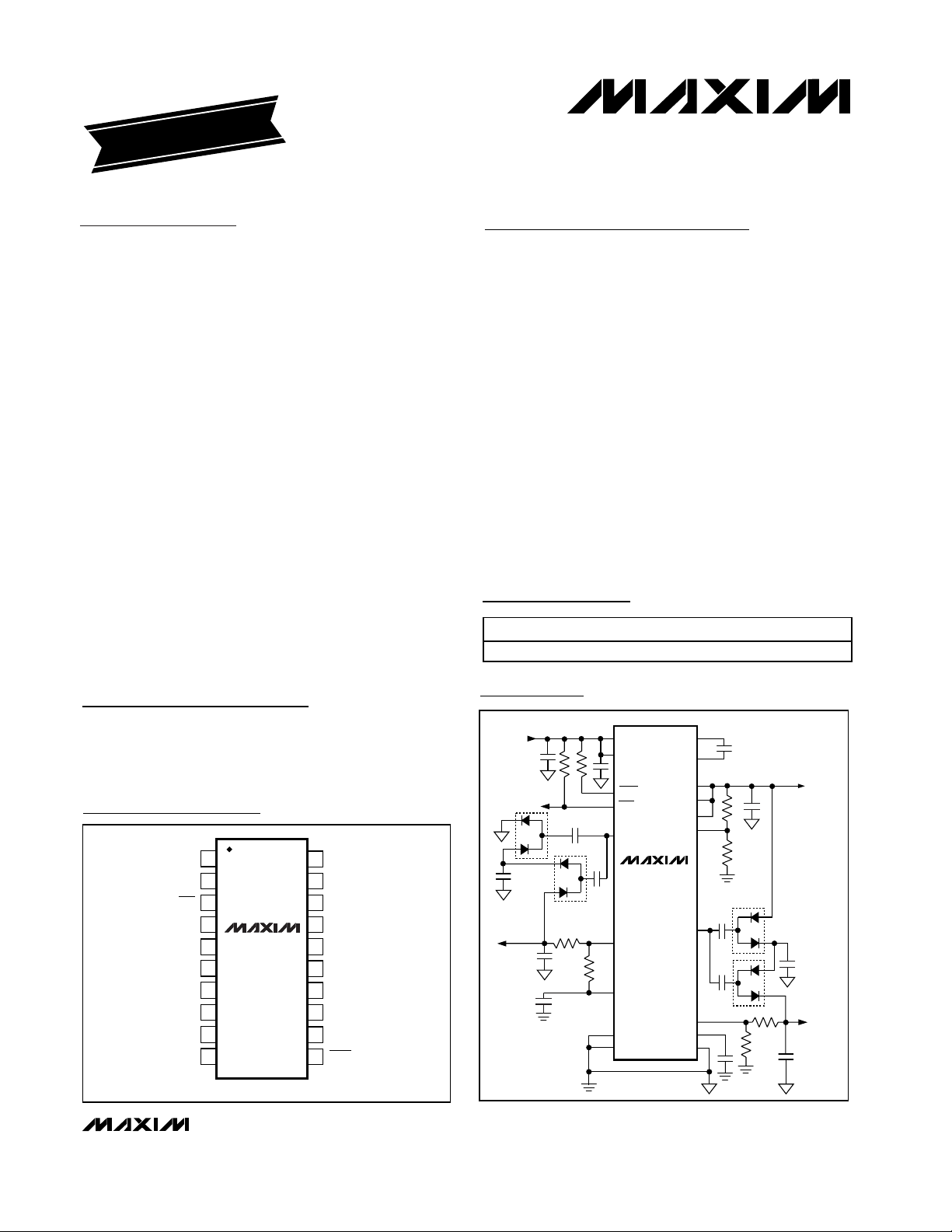
Pin Configuration
19-1788; Rev 0; 10/00
Ordering Information
Features
♦ Adjustable Outputs
Up to +5.5V Main High-Power Output
Up to +35V Positive Charge-Pump Output
Down to -35V Negative Charge-Pump Output
♦ 200kHz to 2MHz Adjustable Switching Frequency
♦ +2.7V to +4.5V Input Supply
♦ Internal Power MOSFETs
♦ 0.1µA Shutdown Current
♦ Internal Soft-Start
♦ Power-Ready Output
♦ Internal Supply Sequencing
♦ Fast Transient Response
♦ Ultra-Thin Solution (No Inductors)
♦ Thin TSSOP Package (1.1mm max)
Applications
TFT Active-Matrix LCDs
Passive-Matrix Displays
Personal Digital Assistants (PDAs)
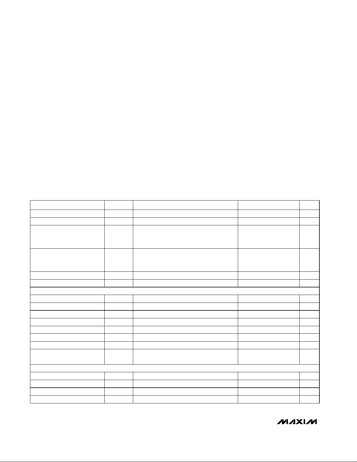
Typical Operating Circuit
EVALUATION KIT
AVAILABLE
TOP VIEW
TGND
TGND
RDY
INTG
GND
FBP
1
2
3
4
5
6
IN
7
8
9
10
20
OUT
19
CXP
18
SUPM
17
CXNFB
MAX1747
16
PGND
15
SUPP
14
DRVP
13
SUPNREF
12
DRVN
11
SHDNFBN
PART TEMP. RANGE PIN-PACKAGE
MAX1747EUP -40°C to +85°C 20 TSSOP
INPUT
TO µC
NEGATIVE
OUTPUT
MAX1747
CXP
CXN
OUT
SUPP
SUPN
DRVP
FBP
INTG
PGND
MAIN OUTPUT
FB
POSITIVE
OUTPUT
SUPM
IN
SHDN
RDY
DRVN
FBN
REF
TGND
GND
TSSOP
Page 2
MAX1747
Triple Charge-Pump TFT LCD
DC-DC Converter
2 _______________________________________________________________________________________
ABSOLUTE MAXIMUM RATINGS
ELECTRICAL CHARACTERISTICS
(VIN= V
SUPM
= +3.0V, V
SUPP
= V
SUPN
= +5V, TGND = PGND = GND, I
SHDN
= 22µA, C
OUT
= 2 ✕4.7µF, C
REF
= 0.22µF, C
INTG
=
1500pF, V
OUT
= +5V, TA= 0°C to +85°C, unless otherwise noted. Typical values are at TA= +25°C.)
Stresses beyond those listed under “Absolute Maximum Ratings” may cause permanent damage to the device. These are stress ratings only, and functional
operation of the device at these or any other conditions beyond those indicated in the operational sections of the specifications is not implied. Exposure to
absolute maximum rating conditions for extended periods may affect device reliability.
IN, SUPM, OUT, TGND to GND................................-0.3V to +6V
SHDN........................................................................-0.3V to +1V
PGND to GND.....................................................................±0.3V
SUPM to IN .........................................................................±0.3V
CXN to PGND.........................................-0.3V to (V
SUPM
+ 0.3V)
CXP to PGND ............................(V
SUPM
- 0.3V) to (V
OUT
+ 0.3V)
DRVN to GND .........................................-0.3V to (V
SUPN
+ 0.3V)
DRVP to GND..........................................-0.3V to (V
SUPP
+ 0.3V)
RDY to GND ...........................................................-0.3V to +14V
SUPP, SUPN to GND..............................................-0.3V to +14V
INTG, REF, FB, FBN, FBP to GND...............-0.3V to (V
IN
+ 0.3V)
Continuous Current into:
SUPM, CXN, CXP, OUT ..............................................±800mA
SUPP, SUPN, DRVN, DRVP........................................±200mA
SHDN...........................................................................+100µA
All Other Pins ....................................................................±10mA
Continuous Power Dissipation (T
A
= +70°C)
20-Pin TSSOP (derate 10.9mW/°C above +70°C) .......879mW
Operating Temperature Range............................-40°C to +85°C
Junction Temperature......................................................+150°C
Storage Temperature Range .............................-65°C to +150°C
Lead Temperature (soldering, 10s) .................................+300°C
)
Input Supply Range V
Input Undervoltage Threshold V
Input Quiescent Supply
Current
PARAMETER SYMBOL CONDITIONS MIN TYP MAX U N IT S
IN
UVLO
IIN +
I
SUPM
VIN falling, 40mV hysteresis (typ) 2.2 2.4 2.6 V
VFB = V
FBP
no load on DRVN and DRVP; CXN
and CXP open
= 1.5V, V
2.7 4.5 V
= -0.2V, V
FBN
OUT
= 5V,
0.9 1.0 mA
Output Quiescent Supply
Current
I
Q(OUT
Shutdown Supply Current V
Operating Frequency f
OSC
VFB = V
no load on DRVN and DRVP; CXN and
CXP open
SHDN
I
SHDN
= 1.5V, V
FBP
= -0.2V, V
FBN
OUT
= 5V,
2.5 4.0 mA
= 0, V
= 5V 0.1 20 µA
SUPM
= 22µA 0.65 1 1.2 MHz
MAIN CHARGE PUMP
Output Voltage Range V
Maximum Output Current I
OU T( M AX ) CX
FB Regulation Voltage V
FB Input Bias Current I
OUT
FB
FB
= 0.47µF 200 mA
VFB = 1.25V -50 +50 nA
4.5 5.5 V
1.237 1.248 1.263 V
Integrator Transconductance 530 µS
FB Power-Ready Trip Level Rising edge 1.09 1.125 1.16 V
FB Fault Trip Level Falling edge 1.100 V
Main Soft-Start Period
4.096
/ F
OSC
NEGATIVE LOW-POWER CHARGE PUMP
SUPN Input Supply Range V
SUPN Quiescent Current I
SUPN
SUPN
SUPN Shutdown Current V
FBN Regulation Voltage V
FBN
V
= -0.2V, no load on DRVN 0.6 0.8 mA
FBN
SHDN
= 0, V
= 13V 0.1 10 µA
SUPN
2.7 13 V
-50 0 +50 mV
s
Page 3
MAX1747
Triple Charge-Pump TFT LCD
DC-DC Converter
_______________________________________________________________________________________ 3
ELECTRICAL CHARACTERISTICS (continued)
(VIN= V
SUPM
= +3.0V, V
SUPP
= V
SUPN
= +5V, TGND = PGND = GND, I
SHDN
= 22µA, C
OUT
= 2 ✕4.7µF, C
REF
= 0.22µF, C
INTG
=
1500pF, V
OUT
= +5V, TA= 0°C to +85°C, unless otherwise noted. Typical values are at TA= +25°C.)
FBN Input Bias Current I
DRVN PCH On-Resistance 36Ω
DRVN NCH On-Resistance
FBN Power-Ready Trip Level Falling edge 80 125 165 mV
FBN Fault Trip Level Rising edge 140 mV
Negative Soft-Start Period
POSITIVE LOW-POWER CHARGE PUMP
SUPP Input Supply Range V
SUPP Quiescent Current I
SUPP Shutdown Current V
FBP Regulation Voltage V
FBP Input Bias Current I
DRVP PCH On-Resistance 36Ω
DRVP NCH On-Resistance
FBP Power-Ready Trip Level Rising edge 1.090 1.125 1.160 V
FBP Fault Trip Level Falling edge 1.100 V
Positive Soft-Start Period
REFERENCE
Reference Voltage V
Reference Undervoltage
Threshold
LOGIC SIGNALS
SHDN Input Low Voltage 0.4 V
SHDN Bias Voltage I
SHDN Bias Voltage Tempco 2 mV/°C
SHDN Input Current Range I
RDY Output Low Voltage I
RDY Output High Leakage V
PARAMETER SYMBOL CONDITIONS MIN TYP MAX U N IT S
V
FBN
SUPP
SUPP
FBP
FBP
REF
SHDN
= -50mV -50 +50 nA
FBN
V
= 50mV 1 5 Ω
FBN
= -50mV 20 kΩ
V
FBN
V
= 1.5V, no load on DRVP 0.6 0.8 mA
FBP
= 0, V
SHDN
V
= 1.5V -50 +50 nA
FBP
V
= 1.20V 1.5 5 Ω
FBP
V
= 1.30V 20 kΩ
FBP
-2µA < I
V
For 200kHz to 2MHz operation 3 65 µA
REF
rising 0.95 1.05 1.18 V
REF
= 22µA 580 724 830 mV
SHDN
= 2mA 0.25 0.5 V
SINK
= 13V 0.01 1 µA
RDY
= 13V 0.1 10 µA
SUPP
< 50µA 1.231 1.25 1.269 V
2.7 13 V
1.20 1.25 1.30 V
2.048/
F
OSC
2.048/
F
OSC
s
s
Page 4
MAX1747
Triple Charge-Pump TFT LCD
DC-DC Converter
4 _______________________________________________________________________________________
ELECTRICAL CHARACTERISTICS
(V
IN
= V
SUPM
= +3.0V, V
SUPP
= V
SUPN
= +5V, TGND = PGND = GND, I
SHDN
= 22µA, C
OUT
= 2 ✕4.7µF, C
REF
= 0.22µF, C
INTG
=
1500pF, V
OUT
= +5V, TA= -40°C to +85°C, unless otherwise noted.) (Note 1)
Input Supply Range V
Input Undervoltage Threshold V
Input Quiescent Supply
Current
PARAMETER SYMBOL CONDITIONS MIN MAX UNITS
IN
UVLO
IIN +
I
SUPM
VIN falling, 40mV hysteresis (typ) 2.2 2.6 V
VFB = V
FBP
no load on DRVN and DRVP; CXN and
CXP open
= 1.5V, V
FBN
= -0.2V, V
OUT
= 5V,
2.7 4.5 V
1.0 mA
Output Quiescent Supply
Current
I
Q(OUT)
Input Shutdown Current V
Operating Frequency f
OSC
VFB = V
no load on DRVN and DRVP; CXN and
CXP open
SHDN
I
SHDN
= 1.5V, V
FBP
= -0.2V, V
FBN
OUT
= 5V,
4.0 mA
= 0, V
= 5V 20 µA
SUPM
= 22µA 0.65 1.2 MHz
MAIN CHARGE PUMP
Output Voltage Range V
Output Current I
OU T ( M AX ) CX
FB Regulation Voltage V
FB Input Bias Current I
OUT
FB
FB
= 0.47µF 200 mA
VFB = 1.25V -50 +50 nA
4.5 5.5 V
1.222 1.271 V
FB Power-Ready Trip Level Rising edge 1.09 1.16 V
NEGATIVE LOW-POWER CHARGE PUMP
SUPN Input Supply Range V
SUPN Quiescent Current I
SUPN
SUPN
SUPN Shutdown Current V
FBN Regulation Voltage V
FBN Input Bias Current I
FBN
FBN
V
= -0.2V, no load on DRVN 0.8 mA
FBN
= 0, V
SHDN
V
= 0 -50 +50 nA
FBN
= 13V 10 µA
SUPN
2.7 13 V
-50 +50 mV
DRVN PCH On-Resistance 6 Ω
V
= 50mV 5 Ω
DRVN NCH On-Resistance
FBN
= -50mV 20 kΩ
V
FBN
FBN Power-Ready Trip Level Falling edge 80 165 mV
POSITIVE LOW-POWER CHARGE PUMP
SUPP Input Supply Range V
SUPP Quiescent Current I
SUPP
SUPP
SUPP Shutdown Current V
FBP Regulation Voltage V
FBP Input Bias Current I
FBP
FBP
V
= 1.5V, no load on DRVP 0.8 mA
FBP
= 0, V
SHDN
V
= 1.5V -50 +50 nA
FBP
= 13V 10 µA
SUPP
2.7 13 V
1.20 1.30 V
DRVP PCH On-Resistance 6 Ω
V
= 1.20V 5 Ω
DRVP NCH On-Resistance
FBP
V
= 1.30V 20 kΩ
FBP
FBP Power-Ready Trip Level Rising edge 1.09 1.16 V
Page 5

MAX1747
Triple Charge-Pump TFT LCD
DC-DC Converter
_______________________________________________________________________________________ 5
ELECTRICAL CHARACTERISTICS (continued)
(V
IN
= V
SUPM
= +3.0V, V
SUPP
= V
SUPM
= +5V, TGND = PGND = GND, I
SHDN
= 22µA, C
OUT
= 2 ✕4.7µF, C
REF
= 0.22µF, C
INTG
=
1500pF, V
OUT
= +5V, TA= -40°C to +85°C, unless otherwise noted.) (Note 1)
Note 1: Specifications from 0°C to -40°C are guaranteed by design, not production tested.
Typical Operating Characteristics
(Circuit of Figure 1, VIN= V
SUPM
= +3.3V, TA= +25°C, unless otherwise noted.)
4.97
4.99
4.98
5.01
5.00
5.02
5.03
0200100 300 400
MAX1747 toc01
I
OUT
(mA)
V
OUT
(V)
MAIN OUTPUT EFFICIENCY
vs. LOAD CURRENT
(MAIN CHARGE PUMP ONLY)
VIN = 3.3V
VIN = 4.0V
VIN = 2.8V
40
60
50
80
70
90
100
0200100 300 400
MAX1747 toc02
I
OUT
(mA)
EFFICIENCY (%)
MAIN OUTPUT EFFICIENCY
vs. LOAD CURRENT
(MAIN CHARGE PUMP ONLY)
V
OUT
= 5V
VIN = 3.3V
VIN = 4.0V
VIN = 2.8V
40
60
50
80
70
90
100
0200100 300 400
MAX1747 toc03
I
OUT
(mA)
EFFICIENCY (%)
MAIN OUTPUT EFFICIENCY
vs. LOAD CURRENT
(MAIN CHARGE PUMP ONLY)
V
OUT
= 5V
VIN = 3.3V
VIN = 4.0V
VIN = 2.8V
V
NEG
= -7V WITH I
NEG
= 10mA
V
POS
= 12V WITH I
POS
= 5mA
PARAMETER SYMBOL CONDITIONS MIN MAX UNITS
REFERENCE
Reference Voltage V
Reference Undervoltage
Threshold
REF
-2µA < I
V
REF
< 50µA 1.222 1.269 V
REF
rising 0.95 1.18 V
LOGIC SIGNALS
Input Low Voltage 0.4 V
SHDN
Bias Voltage I
SHDN
Input Current Range I
SHDN
Output Low Voltage I
RDY
Output High Leakage V
RDY
SHDN
= 22µA 580 900 mV
SHDN
For 200kHz to 2MHz operation 3 65 µA
= 2mA 0.5 V
SINK
= 13V 1 µA
RDY
Page 6

MAX1747
Triple Charge-Pump TFT LCD
DC-DC Converter
6 _______________________________________________________________________________________
Typical Operating Characteristics (continued)
(Circuit of Figure 1, VIN= V
SUPM
= +3.3V, TA= +25°C, unless otherwise noted.)
0
2
4
6
8
10
12
14
16
0 0.5 1.0 1.5 2.0
NO-LOAD SUPPLY CURRENT
vs. SWITCHING FREQUENCY
MAX1747 toc04
FREQUENCY (MHz)
I
CC
+ I
IN
(mA)
0
0.4
1.2
0.8
1.6
2.0
02010 30 40 50
SWITCHING FREQUENCY
vs. I
SHDN
MAX1747 toc05
I
SHDN
(mA)
FREQUENCY (MHz)
9.0
10.0
9.5
11.0
10.5
11.5
12.0
-40 10-15 35 60 85
MAX1747 toc06
TEMPERATURE (°C)
I
IN
+ I
SUPM
(mA)
NO-LOAD SUPPLY CURRENT
vs. TEMPERATURE
VON = 3.3V
R
FREQ
= 120k
Ω
0.85
0.95
0.90
1.05
1.00
1.10
1.15
-40 10-15 356085
MAX1747 toc07
TEMPERATURE (°C)
FREQUENCY (MHz)
SWITCHING FREQUENCY
vs. TEMPERATURE
VON = 3.3V
R
FREQ
= 120k
Ω
20
30
40
50
60
70
80
90
100
0 10203040
NEGATIVE LOW-POWER CHARGE-PUMP
EFFICIENCY vs. LOAD CURRENT
MAX1747 toc08
I
NEG
(mA)
EFFICIENCY (%)
V
SUPN
= 6V
V
SUPN
= 5V
V
SUPN
= 7V
V
NEG
= -7V
-7.1
-7.0
-6.9
-6.8
-6.7
-6.6
-6.5
-6.4
-6.3
0 10203040
NEGATIVE LOW-POWER CHARGE-PUMP
OUTPUT VOLTAGE vs. LOAD CURRENT
MAX1747 toc09
I
NEG
(mA)
V
NEG
(V)
V
SUPN
= 5V
V
SUPN
= 6V
V
SUPN
= 7V
-22
-18
-10
-14
-6
-2
37591113
MAXIMUM NEGATIVE CHARGE-PUMP
OUTPUT VOLTAGE vs. SUPPLY VOLTAGE
MAX1747 toc10
V
SUPN
(V)
V
NEG
(V)
I
NEG
= 10mA
I
NEG
= 1mA
V
NEG(NOMINAL)
= -20V
11.4
11.5
11.6
11.7
11.8
11.9
12.0
12.1
12.2
0 10203040
POSITIVE LOW-POWER CHARGE-PUMP
OUTPUT VOLTAGE vs. LOAD CURRENT
MAX1747 toc12
I
POS
(mA)
V
POS
(V)
V
SUPP
= 7V
V
SUPP
= 6V
V
SUPP
= 5V
20
30
40
50
60
70
80
90
100
0 10203040
POSITIVE LOW-POWER CHARGE-PUMP
EFFICIENCY vs. LOAD CURRENT
MAX1747 toc11
I
POS
(mA)
EFFICIENCY (%)
V
SUPP
= 6V
V
SUPP
= 5V
V
POS
= 12V
V
SUPP
= 7V
Page 7

MAX1747
Triple Charge-Pump TFT LCD
DC-DC Converter
_______________________________________________________________________________________ 7
Typical Operating Characteristics (continued)
(Circuit of Figure 1, VIN= V
SUPM
= +3.3V, TA= +25°C, unless otherwise noted.)
MAXIMUM POSITIVE CHARGE-PUMP
OUTPUT VOLTAGE vs. SUPPLY VOLTAGE
34
V
POS(NOMINAL)
28
22
(V)
POS
V
16
10
4
37591113
RIPPLE WAVEFORM
= 32V
MAX1747 toc15
MAX1747 toc13
V
OUT
20mV/div
V
NEG
10mV/div
V
POS
10mV/div
I
= 1mA
POS
I
= 10mA
POS
V
(V)
SUPP
200mA
100mA
5.05V
4.95V
LOAD TRANSIENT
0
5V
40µs/div
V
= 3.3V, V
IN
R
OUT
C
INTG
= 5.0V
OUT
= 500Ω TO 25
= 1500pF
Ω
STARTUP WAVEFORM (NO LOAD)
2V
0
4V
2V
4V
2V
0
MAX1747 toc14
MAX1747 toc16
I
OUT
100mA/div
V
OUT
50mV/div
V
ON
2V/div
V
CXP
2V/div
V
OUT
2V/div
V
OUT
V
NEG
V
POS
= +5.0V,I
= -7V, I
= +12V, I
NEG
OUT
= 10mA
POS
= 200mA
= 5mA
STARTUP WAVEFORM (200mA LOAD)
2V
0
4V
2V
4V
2V
0
400ns/div
V
= 5V, R
OUT
ON CONNECTED TO SHDN THROUGH
A 58kΩ RESISTOR
1ms/div
= 25Ω (200mA)
OUT
MAX1747 toc17
V
ON
2V/div
V
CXP
2V/div
V
OUT
2V/div
V
= 5V, NO LOAD
OUT
ON CONNECTED TO SHDN THROUGH
A 58kΩ RESISTOR
2V
0
5V
0
-10V
10V
0
V
= 5V, V
MAIN
ON CONNECTED TO SHDN THROUGH
A 58kΩ RESISTOR
1ms/div
POWER-UP SEQUENCE
2ms/div
NEG
= -7V, V
POS
= 12V
MAX1747 toc18
V
ON
2V/div
V
MAIN
5V/div
V
NEG
10V/div
V
POS
10V/div
Page 8

MAX1747
Triple Charge-Pump TFT LCD
DC-DC Converter
8 _______________________________________________________________________________________
Detailed Description
The MAX1747 is an efficient triple-output power supply
for TFT LCD applications. The device contains one
high-power charge pump and two low-power charge
pumps. The MAX1747 charge pumps switch continuously at a constant frequency, so the output noise contains well-defined frequency components, and the
circuit requires much smaller external capacitors for a
given output ripple. The adjustable switching frequency
is set by the current into the shutdown pin (see
Frequency Selection and Shutdown).
The main charge pump uses internal MOSFETs with
low R
ON
to provide high output current. The adjustable
output voltage of the main charge pump can be set up
to 5.5V with external resistors. The dual low-power
charge pumps independently regulate a positive output
Pin Description
PIN NAME FUNCTION
1, 2 TGND Must be connected to ground.
3 RDY Active-Low Open-Drain Output. Indicates all outputs are ready. The RON is 125Ω (typ).
4FB
5 INTG
6IN
7 GND Analog Ground. Connect to power ground (PGND) underneath the IC.
8 REF
9 FBP
10 FBN
11 SHDN
12 DRVN Negative Charge-Pump Driver Output. Output high level is V
13 SUPN
14 DRVP Positive Charge-Pump Driver Output. Output high level is V
15 SUPP
16 PGND Power Ground. Connect to analog ground (GND) underneath the IC.
17 CXN Negative Terminal of the Main Charge-Pump Flying Capacitor
18 SUPM Main Charge-Pump Supply Voltage Input
19 CXP Positive Terminal of the Main Charge-Pump Flying Capacitor
20 OUT
Main Charge-Pump Feedback Input. Regulates to 1.25V nominal. Connect to the center of a
feedback resistive divider between the main output (OUT) and analog ground (GND).
Main Charge-Pump Integrator Output. If used, connect 1500pF to analog ground (GND). To disable
the integrator, connect to GND.
Supply Input. +2.7V to +4.5V input range. Powers only the logic and reference. Bypass to analog
ground (GND) with a 0.1µF capacitor as close to the pin as possible.
Internal Reference Bypass Terminal. Connect a 0.22µF capacitor from this terminal to analog
ground (GND). External load capability to 50µA. REF is disabled in shutdown.
Positive Charge-Pump Feedback Input. Regulates to 1.25V nominal. Connect feedback resistive
divider to analog ground (GND).
Negative Charge-Pump Regulator Feedback Input. Regulates to 0V nominal. Connect feedback
resistive divider to the reference (REF).
Shutdown Input. Drive SHDN through an external resistor. When SHDN is pulled low, the device
turns off and draws only 0.1µA. OUT is also pulled low through an internal 10Ω resistor in shutdown
mode. When current is sourced into SHDN through R
input current sets the oscillator’s switching frequency:
R
(kΩ) = 45.5 (MHz / mA)
FREQ
Negative Charge-Pump Driver Supply Voltage. Bypass to power ground (PGND) with a 0.1µF
capacitor.
Positive Charge-Pump Driver Supply Voltage. Bypass to power ground (PGND) with a 0.1µF
capacitor.
Main Charge-Pump Output. Bypass to power ground (PGND) with 10µF for a 1MHz application
(see Output Capacitor Selection). An internal 10Ω resistor discharges the output when the device
is shut down.
, the device activates, and the SHDN
FREQ
✕
(VON - 0.7V) / f
SUPN
and low level is PGND.
SUPP
(MHz)
OSC
, and low level is PGND.
Page 9

MAX1747
Triple Charge-Pump TFT LCD
DC-DC Converter
_______________________________________________________________________________________ 9
(V
POS
) and a negative output (V
NEG
). These two outputs use external diode and capacitor stages (as many
stages as required) to regulate output voltages above
+35V and under -35V.
A proprietary regulation algorithm minimizes output ripple as well as capacitor sizes for all three charge
pumps. Also included in the MAX1747 are a precision
1.25V reference that sources up to 50µA, shutdown,
power-up sequencing, fault detection, and an activelow open-drain ready output.
Main Charge Pump
During the first half-cycle, the MAX1747 charges the
flying capacitor (CX) by connecting it between the supply voltage (V
SUPM
) and ground (Figure 2). This initial
charge is controlled by the variable N-channel on-resistance. During the second half-cycle, the MAX1747 level
shifts the flying capacitor by stacking the voltage
across CX on top of the supply voltage. This transfers
the sum of the two voltages to the output capacitor
(C
OUT
).
Dual Charge-Pump Regulators
The MAX1747 contains two individual low-power
charge pumps. Using a single stage, the first charge
pump inverts the supply voltage (V
SUPN
) and provides
a regulated negative output voltage. The second
charge pump doubles the supply voltage (V
SUPP
) and
provides a regulated positive output voltage. The
MAX1747 contains internal P-channel and N-channel
MOSFETs to control the power transfer. The internal
MOSFETs switch at a constant frequency set by the
current into the shutdown pin (see Frequency Selection
and Shutdown).
Figure 1. Typical Application Circuit
V
IN
= 3.0V
C
IN
10µF
C6
1.0µF
V
NEG
-7V, 10mA
100k
D3
D4
C10
1.0µF
SUPM
C1
C5
0.1µF
C
REF
0.1µF
C9
0.1µF
49.9k
R6
R7
R
FREQ
100k
D7
D8
R5
280k
0.22µF
IN
RDY
SHDN
DRVN
MAX1747
FBN
REF
TGND
GND
CXP
CXN
OUT
SUPP
SUPN
FB
DRVP
FBP
INTG
PGND
C11
0.1µF
C3
0.1µF
C7
0.1µF
CX
0.47µF
C12
0.1µF
C
INTG
1500pF
V
OUT
+5V, 200mA
C
OUT
(2) 4.7µF
D1
D2
R4
49.9k
D5
D6
432k
R1
150k
R2
49.9k
C4
1.0µF
V
POS
+12V, 5mA
R3
C8
1.0µF
Page 10

MAX1747
Triple Charge-Pump TFT LCD
DC-DC Converter
10 ______________________________________________________________________________________
Negative Charge Pump
During the first half-cycle, the P-channel MOSFET turns
on, and flying capacitor C5 charges to V
SUPN
minus a
diode drop (Figure 3). During the second half-cycle,
the P-channel MOSFET turns off, and the N-channel
MOSFET turns on, level shifting C5. This connects C5 in
parallel with the reservoir capacitor, C6. If the voltage
across C6 minus a diode drop is lower than the voltage
across C5, current flows from C5 to C6 until the diode
(D4) turns off. The amount of charge transferred to the
output is controlled by the variable N-channel RON.
Positive Charge Pump
During the first half-cycle, the N-channel MOSFET turns
on and charges the flying capacitor, C3 (Figure 4). This
initial charge is controlled by the variable N-channel
RON. During the second half-cycle, the N-channel
MOSFET turns off, and the P-channel MOSFET turns
on, level shifting C3 by V
SUPP
volts. This connects C3
in parallel with the reservoir capacitor, C4. If the voltage
across C4 plus a diode drop (V
POS
+ V
DIODE
) is smaller than the level-shifted flying capacitor voltage (VC3+
V
SUPP
), charge flows from C3 to C4 until the diode (D2)
turns off.
Frequency Selection and Shutdown
The shutdown pin (SHDN) on the MAX1747 performs a
dual function: it shuts down the device and determines
the oscillator frequency. The SHDN input looks like a
diode to ground and should be driven through a resistor (Figure 5).
Driving SHDN low forces all three MAX1747 converters
into shutdown mode. When disabled, the supply current drops to 20µA (max) to maximize battery life, and
OUT is pulled to ground through an internal 10Ω resistor. For the low-power charge pumps, the output
capacitance and load current determine the rate at
which each output voltage will decay. The device activates (see Power-up Sequencing) once SHDN is forward biased (minimum of 3µA of current). Do not leave
SHDN floating. For a typical application where shutdown is used only to set the switching frequency, connect SHDN to the input (V
IN
= 3.3V) with a 120kΩ
resistor for a 1MHz switching frequency.
The bias current into SHDN, programmed with an exter-
nal resistor, determines the oscillator frequency (see
Typical Operating Characteristics). To select the frequency, calculate the external resistor value, R
FREQ
,
using the following formula:
R
FREQ
= 45.5 (MHz / mA) ✕(VON– 0.7V) / f
OSC
where R
FREQ
is in kΩ and f
OSC
is in MHz. Program the
frequency in the 200kHz to 2MHz range. This frequency range corresponds to SHDN input currents between
3µA to 65µA. Proper operation of the oscillator is not
guaranteed beyond these limits. Forcing SHDN below
400mV disables the device.
Soft-Start
For the MAX1747, soft-start is achieved by controlling
the rise rate of the output voltage, regardless of output
capacitance or output load, and limited only by the output impedance of the regulator (see Startup Waveforms
Figure 2. Main Charge-Pump Block Diagram
Figure 3. Negative Charge-Pump Block Diagram
= V
V
SUPM
IN
2.7V TO 4.5V
C1
MAX1747
V
OUT
C
OUT
OSC
MAX1747
SUPM
OSC
OUT
CXP
SUPN
DRVN
= 2.7V TO 13V
V
SUPP
C5
D3
D4
CX
gm
C
INTG
INTG
PGND
V
REF
1.25V
CXN
FB
REF
GND
= [1+ (R1/R2)] ✕ V
V
OUT
V
= 1.25V
REF
R1
R2
C
REF
REF
V
NEG
C6
REF
R6
C
REF
V
V
R5
= -(R5/R6) ✕ V
NEG
= 1.25V
REF
FBN
V
REF
1.25V
REF
GND PGND
Page 11

MAX1747
Triple Charge-Pump TFT LCD
DC-DC Converter
______________________________________________________________________________________ 11
in the Typical Operating Characteristics). The main output voltage is controlled to be in regulation within 4096
clock cycles (1/f
OSC
). The negative and positive lowpower charge pumps are controlled to be in regulation
within 2048 clock cycles.
Power-Up Sequencing
Upon power-up or exiting shutdown, the MAX1747
starts a power-up sequence. First, the reference powers up. Then the primary charge pump powers up with
soft-start enabled. Once the main charge pump reaches 90% of its nominal value (VFB> 1.125V), the negative charge pump turns on. When the negative output
voltage reaches approximately 90% of its nominal value
(V
FBN
< 125mV), the positive charge pump starts up.
Finally, when the positive output voltage reaches 90%
of its nominal value (V
FBP
> 1.125V), the active-low
ready signal (RDY) goes low (see Power Ready).
Fault Detection
Once RDY is low, and if any output falls below its fault
detection threshold, RDY goes high impedance.
For the reference, the fault threshold is 1.05V. For the
main charge pump, the fault threshold is 88% of its
nominal value (VFB< 1.1V). For the negative charge
pump, the fault threshold is approximately 88% of its
nominal value (V
FBN
> 140mV). For the positive charge
pump, the fault threshold is 88% of its nominal value
(V
FBP
< 1.1V).
Once an output faults, all outputs later in the power
sequence shut down until the faulted output rises
above its power-up threshold. For example, if the negative charge-pump output voltage falls below the faultdetection threshold, the main charge pump remains
active while the positive charge pump stops switching
and its output voltage decays, depending on output
capacitance and load. The positive charge-pump output will not power up until the negative charge-pump
output voltage rises above its power-up threshold (see
Power-Up Sequencing).
Power Ready
Power ready is an open-drain output. When the powerup sequence is properly completed, the MOSFET turns
on and pulls RDY low with a typical 125Ω R
ON
. If a fault
is detected, the internal open-drain MOSFET appears
as a high impedance. Connect a 100kΩ pullup resistor
between RDY and IN for a logic level output.
Voltage Reference
The voltage at REF is nominally 1.25V. The reference
can source up to 50mA with excellent load regulation
(see Typical Operating Characteristics). Connect a
0.22µF bypass capacitor between REF and GND.
During shutdown, the reference is disabled.
Design Procedure
Efficiency Considerations
The efficiency characteristics of the MAX1747 regulated charge pumps are similar to a linear regulator. They
are dominated by quiescent current at low output currents and by the input voltage at higher output currents
(see Typical Operating Characteristics). Therefore, the
maximum efficiency may be approximated by:
Efficiency ≅ V
OUT
/ (2 ✕V
SUPM
) for the main
charge pump
Efficiency ≅ - V
NEG
/ (V
SUPN
✕
N) for the negative
low-power charge pump
MAX1747
Figure 4. Positive Charge-Pump Block Diagram
Figure 5. Frequency Adjustment
OSC
SUPP
DRVP
VON = V
V
= 2.7V TO 13V
SUPP
C3
D1
D2
MAX1747
OSC
SHDN
IN
R
FREQ
IN
C
IN
FBP
V
REF
1.25V
GND
PGND
R3
R4
V
= [1 + (R3/R4)] ✕ V
POS
V
= 1.25V
REF
V
POS
C4
REF
GND
= k
FREQ
IS IN kΩ, k
IS IN MHz.
OSC
✕
(VON - 0.7V)/f
IS 45.5MHz/mA,
FREQ
OSC
R
R
AND f
FREQ
FREQ
Page 12

MAX1747
Triple Charge-Pump TFT LCD
DC-DC Converter
12 ______________________________________________________________________________________
Efficiency ≅ V
POS
/ [V
SUPP
✕
(N+1)] for the
positive low-power charge pump
where N is the number of charge-pump stages.
Output Voltage Selection
Adjust the main output voltage by connecting a voltage-divider from the output (V
OUT
) to FB and GND (see
Typical Operating Circuit). Adjust the negative lowpower output voltage by connecting a voltage-divider
from the output (V
NEG
) to FBN to REF. Adjust the positive low-power output voltage by connecting a voltagedivider from the output (V
POS
) to FBP to GND. Select
R2, R4, and R6 in the 10kΩ to 200kΩ range. Calculate
the remaining resistors with the following equations:
R1 = R2 [(V
OUT
/ V
REF
) – 1]
R3 = R4 [(V
POS
/ V
REF
) – 1]
R5 = R6 |V
NEG
/ V
REF
|
where V
REF
= 1.25V. V
OUT
may range from 4.5V to
5.5V, V
POS
may range from V
SUPP
to +35V, and V
NEG
may range from 0 to -35V.
Flying Capacitors
Increasing the flying capacitor’s value increases the
output-current capability. Above a certain point, larger
capacitor values lower the secondary pole formed by
the transfer capacitor and switch RON, which destabilizes the output. For the main charge pump, use a
ceramic capacitor based on the following equation:
For the low-power charge pumps, a 0.1µF ceramic
capacitor works well in most applications. Smaller values may be used for lower current applications.
Component suppliers are listed in Table 1.
Output Capacitors
For the main charge pump, use a ceramic capacitor
based on the following equation:
For low-frequency applications (close to 200kHz),
selection of the output capacitor is limited solely by the
switching frequency. However, for high-frequency
applications (close to 2MHz), selection of the output
capacitor is limited by the secondary pole formed by
the flying capacitor and switch on-resistance.
For the low-power charge pumps, the output capacitor
should be anywhere from 5-times to 20-times larger
than the flying capacitor, depending on the ripple tolerance. Increasing the output capacitance or decreasing
the ESR reduces the output ripple voltage and the
peak-to-peak transient voltage.
Input Capacitors
Using an input capacitor with a value equal to or
greater than the output capacitor is recommended.
Place the capacitor as close to the IC as possible. If the
source impedance or inductance of the input supply is
large, additional input bypassing may be required.
For the low-power charge-pump inputs (SUPN and
SUPP), using bypass capacitors with values equal to or
greater than the flying capacitors is recommended.
Place these capacitors as close to the supply voltage
inputs as possible.
Rectifier Diodes
Use Schottky diodes with a current rating greater than
4 times the average output current, and with a voltage
rating of 1.5 times V
SUPP
for the positive charge pump
and V
SUPN
for the negative charge pump.
Integrator Capacitor
The MAX1747 contains an internal current integrator
that improves the DC load regulation but increases the
peak-to-peak transient voltage (see Load-Transient
Waveform in the Typical Operating Characteristics).
Connect a ceramic capacitor between INTG and GND
based on the following equation:
Table 1. Component Suppliers
C
≤
X
F MHz
µ×047.
f
OSC
C
20 2
≥××
OUT X
M
C
Hz
f AND
OSC
µ
×
FHz
f
OSC
M
C
INTG
SUPPLIER PHONE FAX
CAPACITORS
AVX 803-946-0690 803-626-3123
Kemet 408-986-0424 408-986-1442
Sanyo 619-661-6835 619-661-1055
Taiyo Yuden 408-573-4150 408-573-4159
DIODES
Central
International
Rectifier
Motorola 602-303-5454 602-994-6430
Nihon 847-843-7500 847-843-2798
Hz C
×150
≥
516-435-1110 516-435-1824
310-322-3331 310-322-3332
f
OSC
OUT
Page 13

MAX1747
Triple Charge-Pump TFT LCD DC-DC Converter
Maxim cannot assume responsibility for use of any circuitry other than circuitry entirely embodied in a Maxim product. No circuit patent licenses are
implied. Maxim reserves the right to change the circuitry and specifications without notice at any time.
Maxim Integrated Products, 120 San Gabriel Drive, Sunnyvale, CA 94086 408-737-7600 ____________________ 13
© 2000 Maxim Integrated Products Printed USA is a registered trademark of Maxim Integrated Products.
Package Information
PC Board Layout and Grounding
Careful printed circuit layout is important to minimize
ground bounce and noise. First, place the main chargepump flying capacitor less than 0.2in (5mm) from the
CXP and CXN pins with wide traces and no vias. Then
place 0.1µF ceramic bypass capacitors near the
charge-pump input pins (SUPP and SUPN) to the
PGND pin. Keep the charge-pump circuitry as close to
the IC as possible, using wide traces and avoiding vias
when possible. Locate all feedback resistive dividers as
close to their respective feedback pins as possible. The
PC board should feature separate analog and power
ground areas connected at only one point under the IC.
To maximize output power and efficiency, and minimize
output power ripple voltage, use extra-wide power
ground traces, and solder the IC’s power ground pin
directly to it. Avoid having sensitive traces near the
switching nodes and high-current lines.
Refer to the MAX1747 evaluation kit for an example of
proper board layout.
Chip Information
TRANSISTOR COUNT: 2534
TSSOP,NO PADS.EPS
 Loading...