

Page 1
General Description
The MAX1733/MAX1734 step-down DC-DC converters
deliver over 250mA to outputs as low as 1.25V. These
converters use a unique proprietary current-limited control scheme that achieves over 90% efficiency. These
devices maintain extremely low quiescent supply current (40µA), and their high 1.2MHz (max) operating frequency permits small, low-cost external components.
This combination of features makes the MAX1733/
MAX1734 excellent high-efficiency alternatives to linear
regulators in space-constrained applications.
Internal synchronous rectification greatly improves efficiency and eliminates the external Schottky diode
required in conventional step-down converters. Both
devices also include internal digital soft-start to limit
input current upon startup and reduce input capacitor
requirements.
The MAX1733 provides an adjustable output voltage
(1.25V to 2.0V). The MAX1734 provides factory-preset
output voltages (see Selector Guide). Both are available in space-saving 5-pin SOT23 packages.
Applications
Cellular, PCS, and Cordless Telephones
PDAs, Palmtops, and Handy-Terminals
Battery-Powered Equipment
Features
♦ 250mA Guaranteed Output Current
♦ Synchronous Rectifier for Over 90% Efficiency
♦ Tiny 5-Pin SOT23 Package
♦ 40µA Quiescent Supply Current
♦ 0.01µA Logic-Controlled Shutdown
♦ Up to 1.2MHz Switching Frequency
♦ Fixed 1.8V or 1.5V Outputs (MAX1734)
♦ Adjustable Output Voltage (MAX1733)
♦ ±1.5% Initial Accuracy
♦ 2.7V to 5.5V Input Range
♦ Soft-Start Limits Startup Current
MAX1733/MAX1734
Low-Voltage, Step-Down DC-DC Converters
in SOT23
________________________________________________________________ Maxim Integrated Products 1
GND
OUT (FB)
( ) ARE FOR MAX1733 ONLY.
SHDN
15LXIN
MAX1733
MAX1734
SOT23-5
TOP VIEW
2
34
Pin Configuration
OUT
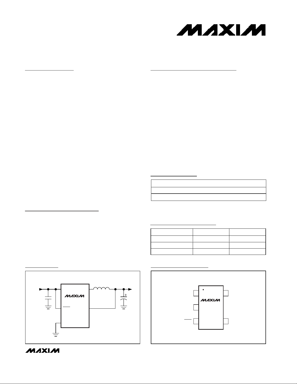
V
OUT
AT
250mA
INPUT
+2.7V TO +5.5V
LX
IN
MAX1734
SHDN
GND
10µH
22µF
2.2µF
Typical Operating Circuit
19-1586; Rev 0; 7/00
For free samples and the latest literature, visit www.maxim-ic.com or phone 1-800-998-8800.
For small orders, phone 1-800-835-8769.
Note: The MAX1734 offers two output voltages. See the Selector
Guide, then insert the proper designator into the blanks above to
complete the part number.
Ordering Information
Selector Guide
PART TEMP. RANGE PIN-PACKAGE
MAX1733EUK-T -40°C to +85°C 5 SOT23-5
M A X1 7 3 4 E U K_ _- T -40°C to +85°C 5 SOT23-5
PART V
MAX1733EUK Adjustable ADKY
MAX1734EUK18 1.8 ADKW
MAX1734EUK15 1.5 ADKX
(V) TOP MARK
OUT
Page 2

MAX1733/MAX1734
Low-Voltage, Step-Down DC-DC Converters
in SOT23
2 _______________________________________________________________________________________
ABSOLUTE MAXIMUM RATINGS
ELECTRICAL CHARACTERISTICS
(VIN= +2.7V to +5.5V, SHDN = IN, TA= 0°C to +85°C. Typical values are at TA= +25°C, unless otherwise noted.)
Stresses beyond those listed under “Absolute Maximum Ratings” may cause permanent damage to the device. These are stress ratings only, and functional
operation of the device at these or any other conditions beyond those indicated in the operational sections of the specifications is not implied. Exposure to
absolute maximum rating conditions for extended periods may affect device reliability.
IN, SHDN to GND .....................................................-0.3V to +6V
OUT, FB, LX to GND....................................-0.3V to (V
IN
+ 0.3V)
OUT Short Circuit to GND ..........................................Continuous
Continuous Power Dissipation (T
A
= +70°C)
5-Pin SOT23 (derate 7.1mW/°C above +70°C)............571mW
Operating Temperature Range ...........................-40°C to +85°C
Junction Temperature......................................................+150°C
Storage Temperature Range .............................-65°C to +150°C
Lead Temperature (soldering, 10s) .................................+300°C
)
Input Voltage Range V
Startup Voltage V
UVLO Threshold V
UVLO Hysteresis 200 mV
Quiescent Supply Current I
Shutdown Supply Current I
Outp ut V ol tag e Range ( MAX 1733) V
Output Voltage Accuracy
(MAX1734)
Load Regulation I
Line Regulation VIN = 2.7V to 5.5V 0 %/V
OUT Sense Current (MAX1734) V
FB Feedback Threshold
(MAX1733)
FB Leakage Current (MAX1733) I
SHDN Input High Voltage V
SHDN Input Low Voltage V
SHDN Leakage Current I
High-Side Current Limit I
Low-Side Current Limit I
High-Side On-Resistance R
Rectifier On-Resistance R
Rectifier Off-Current Threshold I
LX Leakage Current I
LX Reverse Leakage Current I
Minimum On-Time t
Minimum Off-Time
PARAMETER SYMBOL CONDITIONS MIN TYP MAX UNITS
IN
START
UVLO
IN
SHDN
OUT
V
FB
FB
SHDN
LIMP
LIMN
ONP
ONN
LXOFF
LXLEAKVIN
LXLK,R
ON(MIN
t
OFF( M IN)
VIN rising 1.85 1.95
VIN falling 1.55 1.65
No switching, no load (FB/OUT above trip
point)
SHDN = GND 0.01 4 µA
I
= 0, TA = +25°C -1.5 +1.5
OUT
I
= 0 to 250mA -3 +3
OUT
= 0 to 250mA 0 %/mA
OUT
= V
OUT
REG
TA = +25°C, VIN = 3.6V 1.231 1.250 1.269
VIN = 3.6V 1.220 1.280
V
= 1.5V 0.001 0.2 µA
FB
2.7V < VIN < 5.5V 1.6 V
IH
2.7V < VIN < 5.5V 0.4 V
IL
SHDN = GND or IN 0.001 1 µA
I
= -50mA, VIN = 3.0V 0.7 1.4
LX
I
= -50mA, VIN = 5.5V 0.5 1.1
LX
I
= -50mA, VIN = 3.0V 1.0 2
LX
I
= -50mA, VIN = 5.5V 0.8 1.6
LX
= 5.5V, VLX = 0 to V
IN unconnected, VLX = 5.5V, SHDN = GND 0.1 5 µA
VIN = 3.6V 0.28 0.4 0.5 µs
VIN = 3.6V 0.28 0.4 0.5 µs
2.7 5.5 V
40 70 µA
1.25 2.0 V
, VIN = V
= 5V 4 8 µA
SHDN
300 425 535 mA
200 325 430 mA
40 mA
IN
0.1 5 µA
2.0 V
V
%
V
Ω
Ω
Page 3
MAX1733/MAX1734
Low-Voltage, Step-Down DC-DC Converters
in SOT23
_______________________________________________________________________________________ 3
Note 1: All devices are 100% production tested at TA= +25°C. Limits over the operating temperature range are guaranteed by design.
ELECTRICAL CHARACTERISTICS
(VIN= +2.7V to +5.5V, SHDN = IN, TA= -40°C to +85°C, unless otherwise noted.) (Note 1)
)
Input Voltage Range V
Startup Voltage V
UVLO Threshold V
Quiescent Supply Current I
Shutdown Supply Current I
Outp ut V ol tag e Range ( MAX 1733) V
Output Voltage Accuracy
(MAX1734)
OUT Sense Current (MAX1734) I
FB Feedback Threshold
(MAX1733)
FB Leakage Current (MAX1733) I
SHDN Input High Voltage V
SHDN Input Low Voltage V
SHDN Leakage Current I
High-Side Current Limit I
Low-Side Current Limit I
High-Side On-Resistance R
Rectifier On-Resistance R
LX Leakage Current I
LX Reverse Leakage Current I
Minimum On-Time t
Minimum Off-Time
PARAMETER SYMBOL CONDITIONS MIN MAX UNITS
IN
START
UVLO
IN
SHDN
OUT
OUT
V
FB
FB
SHDN
LIMP
LIMN
ONP
ONN
LXLEAKVIN
LXLK,R
ON(MIN
t
OFF( M IN)
VIN rising, 200mV typical hysteresis 1.95
VIN falling 1.55
No switching (FB/OUT above trip point) 70 µA
SHDN = GND 4 µA
= 0 to 250mA -3 +3 %
I
OUT
V
= V
REG
, VIN = V
OUT
VIN = 3.6V 1.210 1.280 V
V
= 1.5V 0.2 µA
FB
2.7V < VIN < 5.5V 1.6 V
IH
2.7V < VIN < 5.5V 0.4 V
IL
SHDN = GND or IN 1 µA
ILX = -50mA, VIN = 3.0V 1.4
ILX = -50mA, VIN = 5.5V 1.1
ILX = -50mA, VIN = 3.0V 2
ILX = -50mA, VIN = 5.5V 1.6
= 5.5V, VLX = 0 to V
IN unconnected, VLX = 5.5V, SHDN = GND 5 µA
= 5V 8 µA
SHDN
IN
2.7 5.5 V
2.0 V
V
1.25 2.0 V
300 565 mA
200 430 mA
Ω
Ω
5 µA
0.25 0.55 µs
0.25 0.55 µs
Page 4

MAX1733/MAX1734
Low-Voltage, Step-Down DC-DC Converters
in SOT23
4 _______________________________________________________________________________________
Typical Operating Characteristics
(CIN= 2.2µF ceramic, C
OUT
= 22µF tantalum, L = 10µH, unless otherwise noted.)
100 1000
30
40
50
60
80
70
90
100
0.1 1 10
EFFICIENCY vs.
LOAD CURRENT (V
OUT
= 1.8V)
LOAD CURRENT (mA)
EFFICIENCY (%)
VIN = 5.0V
VIN = 3.6V
VIN = 2.7V
MAX1733/4-01
100 1000
30
40
50
60
80
70
90
100
0.1 1 10
EFFICIENCY vs.
LOAD CURRENT (V
OUT
= 1.5V)
MAX1733/4-02
LOAD CURRENT (mA)
EFFICIENCY (%)
VIN = 5.0V
VIN = 3.6V
VIN = 2.7V
46
48
50
52
54
56
58
60
62
2.5 3.53.0 4.0 4.5 5.0 5.5
NO-LOAD SUPPLY CURRENT
vs. SUPPLY VOLTAGE
MAX1733/4-03
SUPPLY VOLTAGE (V)
SUPPLY CURRENT (µA)
V
OUT
= 1.5V, TA = -40°C
V
OUT
= 1.5V, TA = +25°C
V
OUT
= 1.8V, TA = +85°C
V
OUT
= 1.8V, TA = +25°C
3.0
-3.0
0.1 10 1001 1000
OUTPUT ACCURACY vs.
LOAD CURRENT (V
OUT
= 1.8V)
MAX1733/4-04
LOAD CURRENT (mA)
OUTPUT ACCURACY (%)
-2.0
-1.0
0
1.0
2.0
VIN = 3.6V, TA = -40°C
VIN = 5.0V, TA = +25°C
VIN = 3.6V, TA = +85°C
VIN = 2.7V, TA = +25°C
3.0
-3.0
0.1 10 10011000
OUTPUT ACCURACY vs.
LOAD CURRENT (V
OUT
= 1.5V)
MAX1733/4-05
LOAD CURRENT (mA)
OUTPUT ACCURACY (%)
-2.0
-1.0
0
1.0
2.0
VIN = 3.6V, TA = -40°C
VIN = 2.7V, TA = +25°C
VIN = 3.6V, TA = +85°C
VIN = 5.0V, TA = +25°C
1.50
1.25
1.00
0.75
0.50
2.7 3.33.0 3.6 3.9 4.2
SWITCHING FREQUENCY
vs. SUPPLY VOLTAGE
MAX1733/4-06
SUPPLY VOLTAGE (V)
SWITCHING FREQUENCY (MHz)
V
OUT
= 1.8V
V
OUT
= 1.5V
I
LOAD
= 50mA TO 250mA
LIGHT-LOAD SWITCHING WAVEFORMS
MAX1733/4-07
400ns/div
V
LX
2V/div
V
OUT
AC-COUPLED
20mV/div
VIN = 3.6V, V
OUT
= 1.8V, I
LOAD
= 20mA
HEAVY-LOAD SWITCHING WAVEFORMS
MAX1733/4-08
400ns/div
V
LX
2V/div
V
OUT
AC-COUPLED
20mV/div
VIN = 3.6V, V
OUT
= 1.8V, I
LOAD
= 200mA
Page 5

MAX1733/MAX1734
Low-Voltage, Step-Down DC-DC Converters
in SOT23
_______________________________________________________________________________________ 5
Typical Operating Characteristics (continued)
(CIN= 2.2µF ceramic, C
OUT
= 22µF tantalum, L = 10µH, unless otherwise noted.)
LOAD-TRANSIENT RESPONSE
MAX1733/4-12
4µs/div
V
OUT
AC-COUPLED
50mV/div
I
LOAD
100mA/div
VIN = 3.6V, V
OUT
= 1.8V, I
LOAD
= 20mA TO 200mA
LIGHT-LOAD LINE-TRANSIENT RESPONSE
MAX1733/4-10
4µs/div
V
OUT
AC-COUPLED
50mV/div
V
IN
AC-COUPLED
200mV/div
VIN = 3.4V TO 3.8V, V
OUT
= 1.8V, I
LOAD
= 20mA
HEAVY-LOAD LINE-TRANSIENT RESPONSE
MAX1733/4-11
4µs/div
V
OUT
AC-COUPLED
50mV/div
V
IN
AC-COUPLED
200mV/div
VIN = 3.4V TO 3.8V, V
OUT
= 1.8V, I
LOAD
= 200mA
SOFT-START AND SHUTDOWN RESPONSE
MAX1733/4-09
200µs/div
V
OUT
1V/div
VIN = 3.6V, V
OUT
= 1.8V, R
LOAD
= 7Ω
V
SHDN
5V/div
I
IN
100mA/div
Pin Description
PIN NAME FUNCTION
1IN
2 GND Ground
3 SHDN
FB
4
OUT MAX1734 Voltage Sense Input. OUT is connected to an internal voltage-divider.
5 LX Inductor Connection
Supply Voltage Input. Input range from +2.7V to +5.5V. Bypass with a 2.2µF ceramic capacitor to
GND.
Active-Low Shutdown Input. Connect SHDN to IN for normal operation. In shutdown, LX becomes
high impedance and quiescent current drops to 0.01µA.
MAX1733 Voltage Feedback Input. FB regulates to 1.25V nominal. Connect FB to an external
voltage-divider between the output voltage and GND.
Page 6

MAX1733/MAX1734
Detailed Description
The MAX1733/MAX1734 step-down DC-DC converters
deliver over 250mA to outputs as low as 1.25V. They
use a unique proprietary current-limited control scheme
that maintains extremely low quiescent supply current
(40µA), and their high 1.2MHz (max) operating frequency permits small, low-cost external components. Figure
2 is a simplified functional diagram.
Control Scheme
The MAX1733/MAX1734 use a proprietary, current-limited control scheme to ensure high-efficiency, fast transient response, and physically small external
components. This control scheme is simple: when the
output voltage is out of regulation, the error comparator
begins a switching cycle by turning on the high-side
switch. This switch remains on until the minimum ontime of 400ns expires and the output voltage regulates
or the current-limit threshold is exceeded. Once off, the
high-side switch remains off until the minimum off-time
of 400ns expires and the output voltage falls out of regulation. During this period, the low-side synchronous
rectifier turns on and remains on until either the highside switch turns on again or the inductor current
approaches zero. The internal synchronous rectifier
eliminates the need for an external Schottky diode.
This control scheme allows the MAX1733/MAX1734 to
provide excellent performance throughout the entire
load-current range. When delivering light loads, the
high-side switch turns off after the minimum on-time to
reduce peak inductor current, resulting in increased
efficiency and reduced output voltage ripple. When
delivering medium and higher output currents, the
MAX1733/MAX1734 extend either the on-time or the offtime, as necessary to maintain regulation, resulting in
nearly constant frequency operation with high efficiency and low output voltage ripple.
Shutdown Mode
Connecting SHDN to GND places the MAX1733/
MAX1734 in shutdown mode and reduces supply current to 0.01µA. In shutdown, the control circuitry, internal switching MOSFET, and synchronous rectifier turn
off and LX goes high impedance. Connect SHDN to IN
for normal operation.
Soft-Start
The MAX1733/MAX1734 have internal soft-start circuitry
that limits current draw at startup, reducing transients on
the input source. Soft-start is particularly useful for higher
impedance input sources, such as Li+ and alkaline cells.
Soft-start is implemented by starting with the current limit
at 25% of its full current value and gradually increasing it
in 25% steps until the full current limit is reached. See
Soft-Start and Shutdown Response in the Typical
Operating Characteristics section.
Design Information
Setting the Output Voltage (MAX1733)
Select an output voltage for the MAX1733 by connecting FB to a resistive divider between the output and
Low-Voltage, Step-Down DC-DC Converters
in SOT23
6 _______________________________________________________________________________________
Figure 1. MAX1733 Typical Application Circuit
Figure 2. Simplified Functional Diagram
INPUT
+2.7V TO +5.5V
C1
2.2µF
IN
SHDN
GND
LX
MAX1733
FB
L1
10µH
R1
R2
V
OUT
C2
22µF
IN
MAX1733
MAX1734
DIGITAL
SOFT-START
SHDN
( ) ARE FOR MAX1733 ONLY.
SHUTDOWN
CONTROL
GND
CURRENT
CONTROL
LOGIC
LIMIT
P
LX
N
OUT (FB)
V
REF
Page 7

GND (Figure 1). Choose R2 to be less than 50kΩ:
where V
REF
= 1.25V.
Inductor Selection
The MAX1733/MAX1734 are optimized to use a 10µH
inductor over the entire operating range. A 300mA
rated inductor is enough to prevent saturation for output currents up to 250mA. Saturation occurs when the
inductor’s magnetic flux density reaches the maximum
level the core can support and inductance falls.
Choose a low DC-resistance inductor to improve efficiency. Tables 1 and 3 list some suggested inductors
and suppliers.
Capacitor Selection
The MAX1733/MAX1734 require output voltage ripple
(approximately 30mVp-p) for stable switching behavior.
Use a 10µF to 47µF tantalum output capacitor with
about 200mΩ to 300mΩ ESR to provide stable switching while minimizing output ripple. Choose input and
output capacitors to filter inductor currents for acceptable voltage ripple. The input capacitor reduces peak
currents and noise at the voltage source. Input capacitors must meet the input ripple requirements and voltage rating. Use the following equation to calculate the
maximum RMS input current:
Tables 2 and 3 list some suggested capacitors and
suppliers.
Using Ceramic C
OUT
with MAX1733
The circuit of Figure 3 is designed to allow the use of
ceramic output capacitors with the MAX1733.
Feedback is derived from the LX pin instead of the output to remove the effects of phase lag in the feedback
loop. Compared to the standard applications circuit,
there are three benefits: 1) availability of ceramic vs.
tantalum; 2) size of 2.2µF 0805 vs. 22µF A-case; 3) output ripple less than 10mVp-p vs. greater than 30mVp-p.
Increase the output capacitance to 4.7µF to further
reduce the output ripple. Note that this circuit exhibits
load regulation equal to the series resistance of the
inductor multiplied by the load current. This small
amount of load regulation is helpful in reducing overshoot of the output voltage during load transients.
MAX1733/MAX1734
Low-Voltage, Step-Down DC-DC Converters
in SOT23
_______________________________________________________________________________________ 7
Table 1. Suggested Inductors
Table 2. Suggested Capacitors
Table 3. Component Suppliers
Figure 3. Using a Ceramic Output Capacitor with the MAX1733
INDUCTOR VALUE
(µH)
10 Sumida
10 Coilcraft DT1608C-103
CAPACITOR
TYPE
Tantalum
(22µF)
Ceramic
(2.2µF)
MANUFACTURER
MANUFACTURER
Taiyo Yuden LMK212BJ225MG
AVX TAJA226M006R
PART
NUMBER
CR43-100
CDRH4D18-100
PART
NUMBER
RR
12 1=× −
V
V
OUT
REF
COMPANY PHONE FAX
AVX 843-946-0238 843-626-3123
Coilcraft 847-639-6400 847-639-1469
Kemet 408-986-0424 408-986-1442
Murata 814-237-1431 814-238-0490
Sumida
Taiyo Yuden 408-573-4150 408-573-4159
USA 847-956-0666 847-956-0702
Japan 81-3-3607-5111 81-3-3607-5144
12/
I
RMS
I V V OUT
OUT OUT IN
=
()
V
IN
−
IN
Li+
2.7V TO 4.2V
2.2µF
X7R
MAX1733
GND
SHDN
OFFON
LX
FB
10µH
30k
1000pF
68k
OUTPUT
1.8V at 250mA
2.2µF
X7R
Page 8
MAX1733/MAX1734
Low-Voltage, Step-Down DC-DC Converters
in SOT23
Maxim cannot assume responsibility for use of any circuitry other than circuitry entirely embodied in a Maxim product. No circuit patent licenses are
implied. Maxim reserves the right to change the circuitry and specifications without notice at any time.
8 _____________________Maxim Integrated Products, 120 San Gabriel Drive, Sunnyvale, CA 94086 408-737-7600
© 2000 Maxim Integrated Products Printed USA is a registered trademark of Maxim Integrated Products.
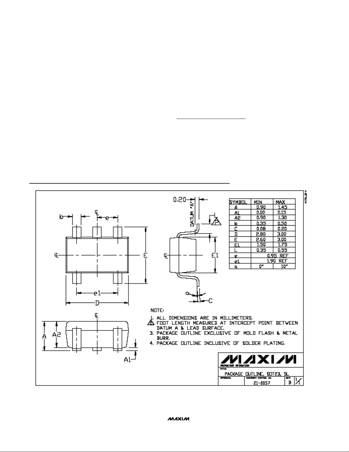
Package Information
Layout Considerations
High switching frequencies make PC board layout a
very important part of design. Good design minimizes
excessive EMI on the feedback paths and voltage gradients in the ground plane, both of which can result in
instability or regulation errors. Connect the inductor,
input filter capacitor, and output filter capacitor as
close to the device as possible, and keep their traces
short, direct, and wide. Connect their ground pins at a
single common node in a star ground configuration.
The external voltage-feedback network should be very
close to the FB pin, within 0.2 inches (5mm). Keep
noisy traces, such as the LX trace, away from the volt-
age-feedback network; also keep them separate, using
grounded copper. The MAX1733/MAX1734 evaluation
kit data sheet includes a proper PC board layout and
routing scheme.
Chip Information
TRANSISTOR COUNT: 1190
PROCESS: BiCMOS
 Loading...