

Page 1
General Description
The MAX1730 regulated step-down charge pump generates up to 50mA at fixed output voltages of 1.8V or
1.9V from an input voltage in the 2.7V to 5.5V range.
Specifically designed to provide high-efficiency logic
supplies in applications that demand a compact
design, the MAX1730 employs fractional conversion
techniques to provide efficiency exceeding that of a linear regulator.
The MAX1730 operates at up to 2MHz, permitting the
use of small 0.22µF flying capacitors while maintaining
low 75µA quiescent supply current. Proprietary softstart circuitry prevents excessive current from being
drawn from the supply during startup, making the
MAX1730 compatible with higher impedance sources
such as alkaline and lithium-ion cells.
The MAX1730 is available in a space-saving 10-pin
µMAX package that is only 1.09mm high and occupies
one-half the area of an 8-pin SO.
Applications
Low-Voltage Logic Supplies
Wireless Handsets
PDAs
PC Cards
Hand-Held Instruments
Features
♦ > 85% Peak Efficiency
♦ 50mA Guaranteed Output Current
♦ Dual-Mode 1.8V or 1.9V Output
♦ ±3% Output Voltage Accuracy
♦ Up to 2MHz Operating Frequency
♦ Small 0.22µF Capacitors
♦ No Inductor Required
♦ 2.7V to 5.5V Input Voltage Range
♦ Output Disconnects from Input in Shutdown Mode
♦ Small 10-Pin µMAX Package (1.09mm max height)
MAX1730
50mA Regulated Step-Down Charge Pump
for 1.8V or 1.9V Logic
________________________________________________________________ Maxim Integrated Products 1
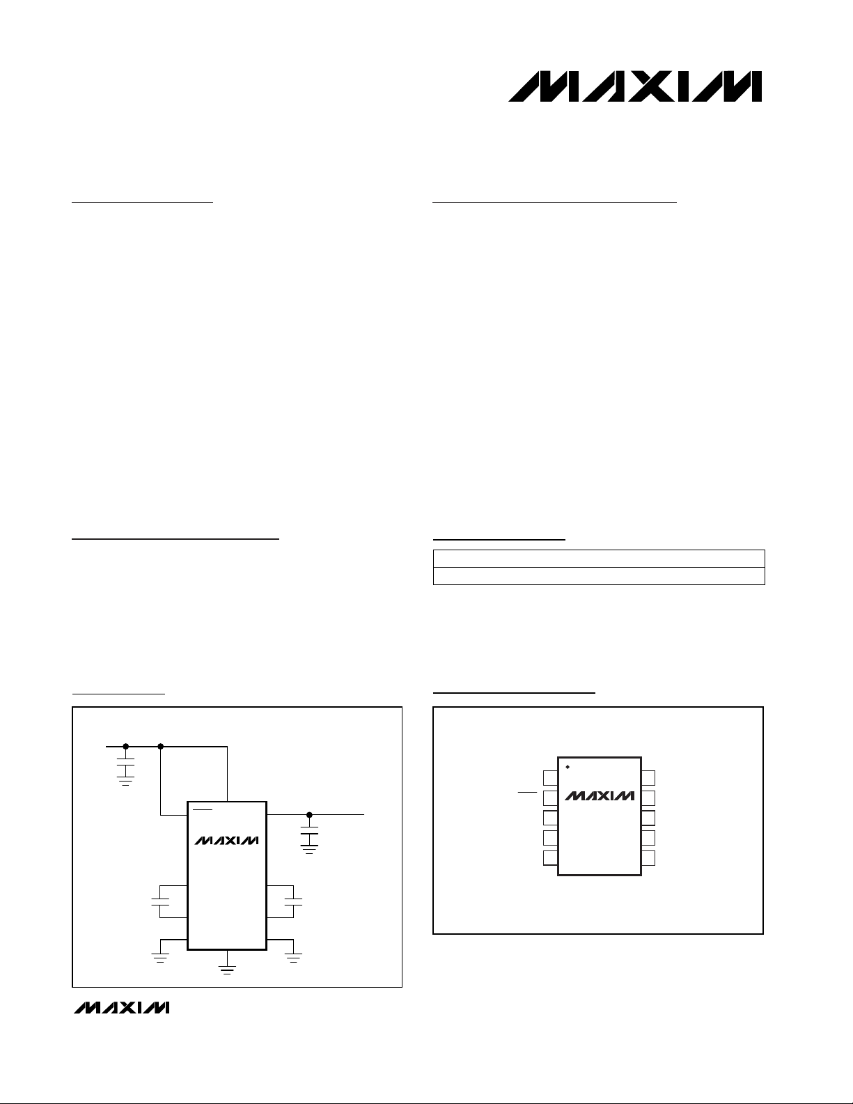
Typical Operating Circuit
19-1618; Rev 0; 4/00
PART
MAX1730EUB -40°C to +85°C
TEMP. RANGE PIN-PACKAGE
10 µMAX
Pin Configuration
Ordering Information
For free samples and the latest literature, visit www.maxim-ic.com or phone 1-800-998-8800.
For small orders, phone 1-800-835-8769.
10
IN
9
MAX1730
µMAX
OUT
8
C2P
7
C2NC1N
PGNDGND
6
INPUT
2.7V TO 5.5V
1µF
0.22µF
TOP VIEW
1
FB
OUTPUT
OUT
C2P
C2N
1.8V OR 1.9V, UP TO 50mA
4.7µF
0.22µF
IN
SHDN
MAX1730
C1P
C1N
FB
GND
PGND
SHDN
C1P
2
3
4
5
Page 2
MAX1730
50mA Regulated Step-Down Charge Pump
for 1.8V or 1.9V Logic
2 _______________________________________________________________________________________
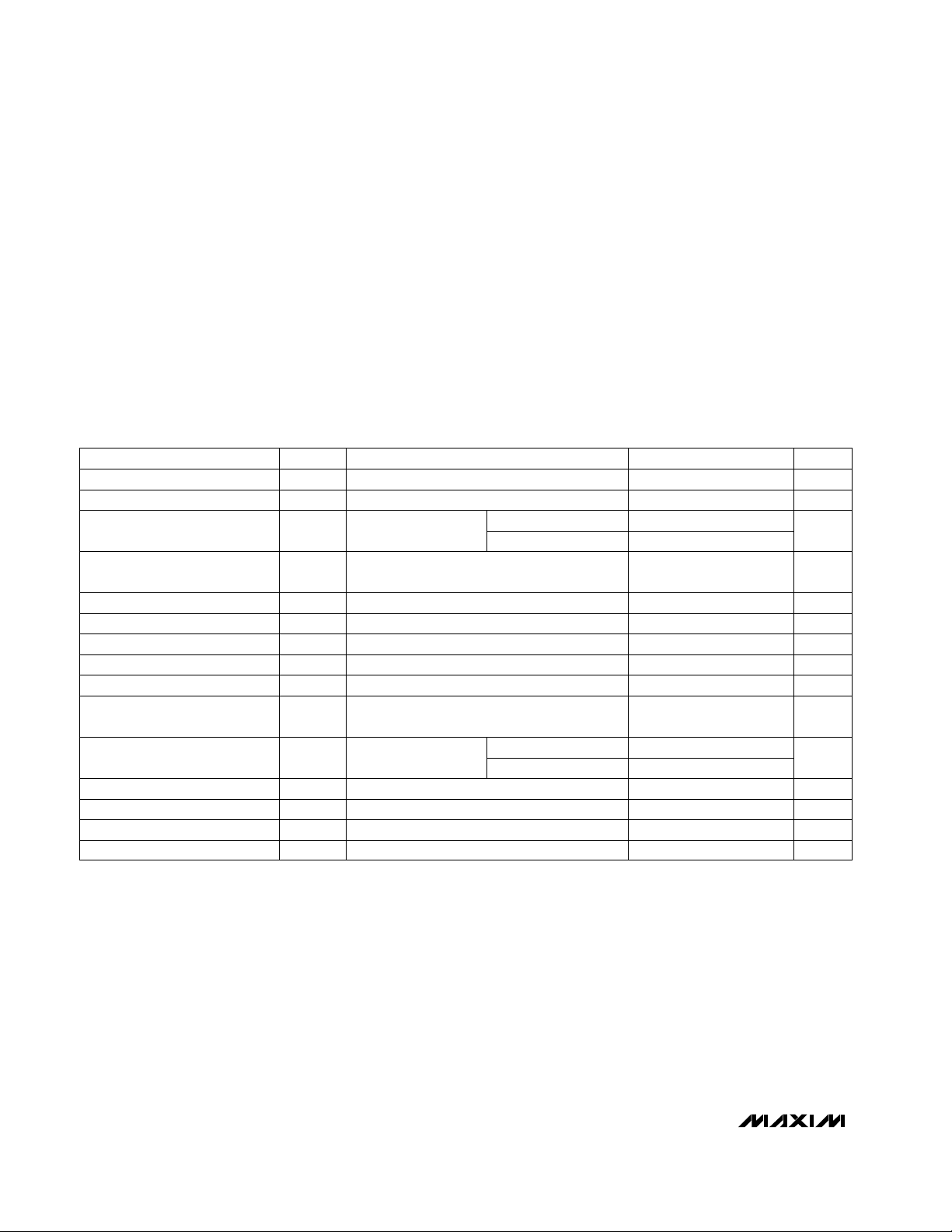
ABSOLUTE MAXIMUM RATINGS
ELECTRICAL CHARACTERISTICS
(VIN= +3.6V, FB = GND, SHDN = IN, TA= 0°C to +85°C, unless otherwise noted. Typical values are at TA= +25°C.)
Stresses beyond those listed under “Absolute Maximum Ratings” may cause permanent damage to the device. These are stress ratings only, and functional
operation of the device at these or any other conditions beyond those indicated in the operational sections of the specifications is not implied. Exposure to
absolute maximum rating conditions for extended periods may affect device reliability.
IN, OUT, SHDN, FB to GND .....................................-0.3V to +6V
C1P, C1N, C2P, C2N to GND......................-0.3V to (V
IN
+ 0.3V)
GND to PGND.....................................................................±0.3V
Output Short-Circuit Duration ........................................Indefinite
Continuous Power Dissipation (T
A
= +70°C)
10-Pin µMAX (derate 5.6mW/°C above +70°C) ...........444mW
Junction Temperature......................................................+150°C
Operating Temperature Range ...........................-40°C to +85°C
Storage Temperature Range .............................-65°C to +150°C
Lead Temperature Range (soldering, 10s)......................+300°C
FB = GND
FB = IN
SHDN = IN or GND
VIN= 2.7V to 5.5V
VIN= 2.7V to 5.5V
Falling edge (100mV hysteresis)
V
OUT
= GND
V
IN
= 4.2V, SHDN = GND, V
OUT
= 1.8V or GND
SHDN = IN
OUT forced to 1.8V, VIN= 1.8V to 5.5V,
SHDN = GND
VIN= 2.7V to 5.5V,
I
OUT
= 0 to 50mA
CONDITIONS
µA
-1 1
I
SHDN
Shutdown Logic Input Current
V
0.6
V
IL
SHDN Logic Input Low Voltage
V
1.4
V
IH
SHDN Logic Input High Voltage
ms
4.1
Startup Timer
V
IN
Transition Voltage
(V
IN
Rising)
°C
15
Thermal Shutdown Threshold
Hysteresis
°C
150
Thermal Shutdown Threshold
MHz
1.5 2.0 2.5
Oscillator Frequency
V
1.746 1.80 1.854
V
OUT
Output Voltage
V
2.3 2.6
V
2.7 5.5
V
IN
Input Voltage Range
Input Undervoltage Lockout
mA
45 125
Output Short-Circuit Current
µA
15
Shutdown Supply Current
µA
75 150
No-Load Supply Current
µA
15
Output Leakage Current
1.843 1.90 1.957
UNITSMIN TYP MAXSYMBOLPARAMETER
V
4.00 4.12 4.30
3.1 3.2 3.35
From 2:3 to 1:2
From 1:1 to 2:3
FB = GND
Page 3
MAX1730
50mA Regulated Step-Down Charge Pump
for 1.8V or 1.9V Logic
_______________________________________________________________________________________ 3
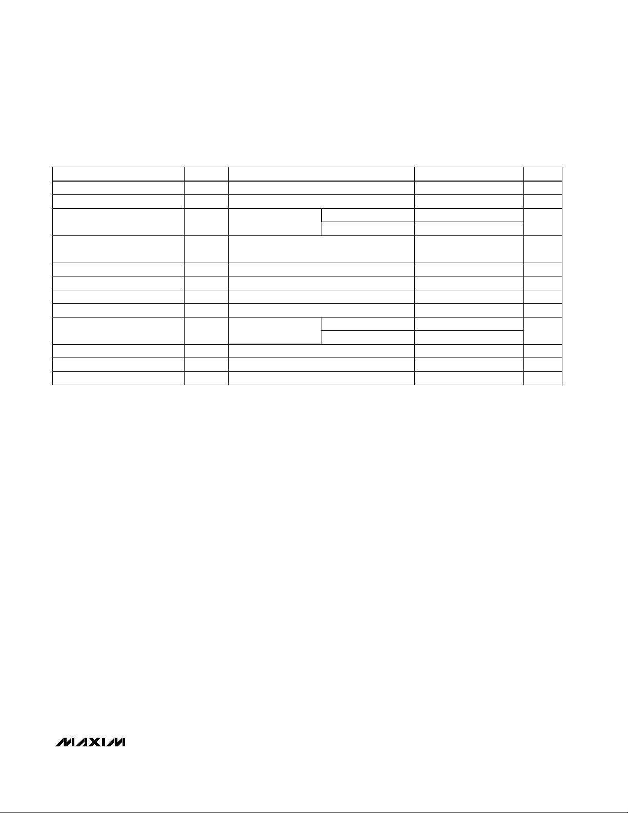
ELECTRICAL CHARACTERISTICS
(VIN= +3.6V, FB = GND, SHDN = IN, TA= -40°C to +85°C, unless otherwise noted.) (Note 1)
Note 1: Specifications to -40°C are guaranteed by design, not production tested.
SHDN = IN or GND
VIN= 2.7V to 5.5V
VIN= 2.7V to 5.5V
Falling edge (100mV hysteresis)
FB = GND
V
OUT
= GND
V
IN
= 4.2V, SHDN = GND
SHDN = IN
OUT forced to 1.8V, VIN= 1.8V to 5.5V,
SHDN = GND
VIN= 2.7V to 5.5V,
I
OUT
= 0 to 50mA
CONDITIONS
FB = GND
FB = IN
µA
-1 1
I
SHDN
Shutdown Logic Input Current
V
0.6
V
IL
SHDN Logic Input Low Voltage
V
1.4
V
IH
SHDN Logic Input High Voltage
V
3.1 3.35
VINTransition Voltage
(VINRising)
MHz
1.5 2.5
fOscillator Frequency
V
1.746 1.854
V
OUT
Output Voltage
V
2.3 2.6
V
2.7 5.5
V
IN
Input Voltage Range
Input Undervoltage Lockout
mA
125
Output Short-Circuit Current
µA
5
Shutdown Supply Current
µA
150
No-Load Supply Current
µA
5
Output Leakage Current
1.843 1.957
From 1:1 to 2:3
UNITSMIN MAXSYMBOLPARAMETER
From 2:3 to 1:2
4.00 4.30
Page 4
MAX1730
50mA Regulated Step-Down Charge Pump
for 1.8V or 1.9V Logic
4 _______________________________________________________________________________________
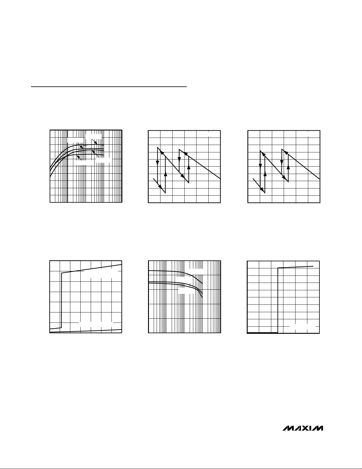
Typical Operating Characteristics
(VIN= +3.6V, FB = GND, SHDN = IN, CIN= 1µF, C1 = C2 = 0.22µF, C
OUT
= 4.7µF, TA= +25°C, unless otherwise noted.)
0.1 101 100 1000
EFFICIENCY
vs. OUTPUT CURRENT
MAX1730 TOC01
OUTPUT CURRENT (mA)
EFFICIENCY (%)
100
90
80
70
60
0
10
30
20
50
40
VIN = 5.0V
VIN = 2.7V
VIN = 3.6V
VIN = 3.3V
50
65
60
55
70
75
80
85
90
95
100
2.5 3.53.0 4.0 4.5 5.0 5.5
EFFICIENCY vs. INPUT VOLTAGE
MAX1730 TOC02
INPUT VOLTAGE (V)
EFFICIENCY (%)
I
OUT
= 25mA
50
65
60
55
70
75
80
85
90
95
100
2.5 3.53.0 4.0 4.5 5.0 5.5
EFFICIENCY vs. INPUT VOLTAGE
MAX1730 TOC02
INPUT VOLTAGE (V)
EFFICIENCY (%)
I
OUT
= 50mA
0
20
10
40
30
60
50
70
2.0 3.0 3.52.5 4.0 4.5 5.0 5.5
INPUT CURRENT vs. INPUT VOLTAGE
MAX1730 TOC04
INPUT VOLTAGE (V)
INPUT CURRENT (µA)
SHUTDOWN CURRENT
NO-LOAD
SUPPLY CURRENT
0.1 101 100 1000
OUTPUT VOLTAGE
vs. OUTPUT CURRENT
MAX1730 TOC05
OUTPUT CURRENT (mA)
OUTPUT VOLTAGE (V)
1.85
1.75
1.77
1.79
1.83
1.81
VIN = 5.0V
VIN = 2.7V
VIN = 3.3V
0
0.4
0.2
0.8
0.6
1.2
1.4
1.6
1.8
1.0
2.0
0231 456
OUTPUT VOLTAGE vs. INPUT VOLTAGE
MAX1730 TOC06
INPUT VOLTAGE (V)
OUTPUT VOLTAGE (V)
I
OUT
= 0 to 50mA
Page 5
MAX1730
50mA Regulated Step-Down Charge Pump
for 1.8V or 1.9V Logic
_______________________________________________________________________________________ 5
Typical Operating Characteristics (continued)
(VIN= +3.6V, FB = GND, SHDN = IN, CIN= 1µF, C1 = C2 = 0.22µF, C
OUT
= 4.7µF, TA= +25°C, unless otherwise noted.)
Pin Description
Output. Bypass to GND with a 4.7µF or greater capacitor.OUT9
Input Supply. Connect to a +2.7V to +5.5V supply. Bypass to GND with a 1µF ceramic capacitor as close to
the IC as possible.
IN10
GroundGND5
Power GroundPGND6
C2 Flying Capacitor Negative ConnectionC2N7
C2 Flying Capacitor Positive ConnectionC2P8
C1 Flying Capacitor Negative ConnectionC1N4
C1 Flying Capacitor Positive ConnectionC1P3
PIN
Active-Low Shutdown Input. Connect to logic control or to IN for normal operation. OUT disconnects from the
input in shutdown and goes to high impedance.
SHDN
2
Feedback Input. Connect FB to GND for a 1.8V output. Connect FB to IN for a 1.9V output. Do not leave FB
unconnected.
FB1
FUNCTIONNAME
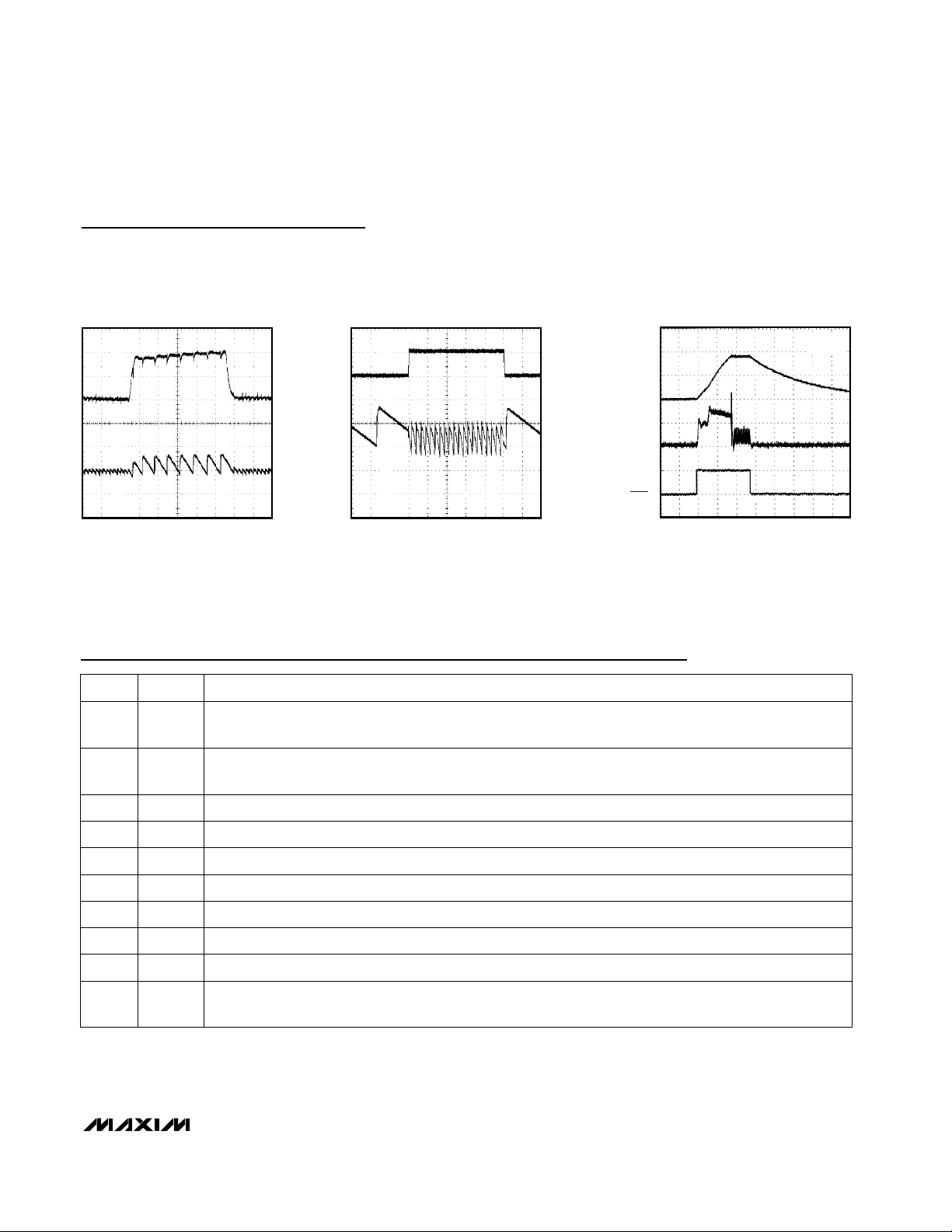
LINE-TRANSIENT RESPONSE
10µs/div
MAX1730 TOC07
4V
V
IN
3V
V
OUT
AC-COUPLED
50mV/div
LOAD-TRANSIENT RESPONSE
10µs/div
MAX1730 TOC08
50mA
I
OUT
5mA
V
OUT
AC-COUPLED
20mV/div
50mA/div
STARTUP AND SHUTDOWN RESPONSE
V
O
1V/div
I
IN
V
SHDN
5V/div
MAX1730 TOC09
RL = 72Ω
100µs/div
Page 6
MAX1730
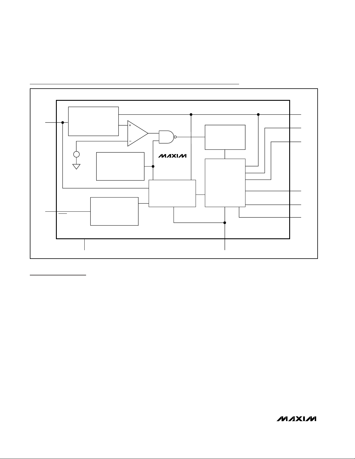
Detailed Description
The MAX1730 step-down charge pump automatically
switches between charge pump configurations (Figures
1, 2, and 3) and utilizes pulse-skipping pulse-frequency
modulation (PFM) to provide a regulated output voltage
with high efficiency. The output voltage is pin-selectable
to 1.8V or 1.9V. The MAX1730 accepts inputs between
2.7V and 5.5V and guarantees up to 50mA output current.
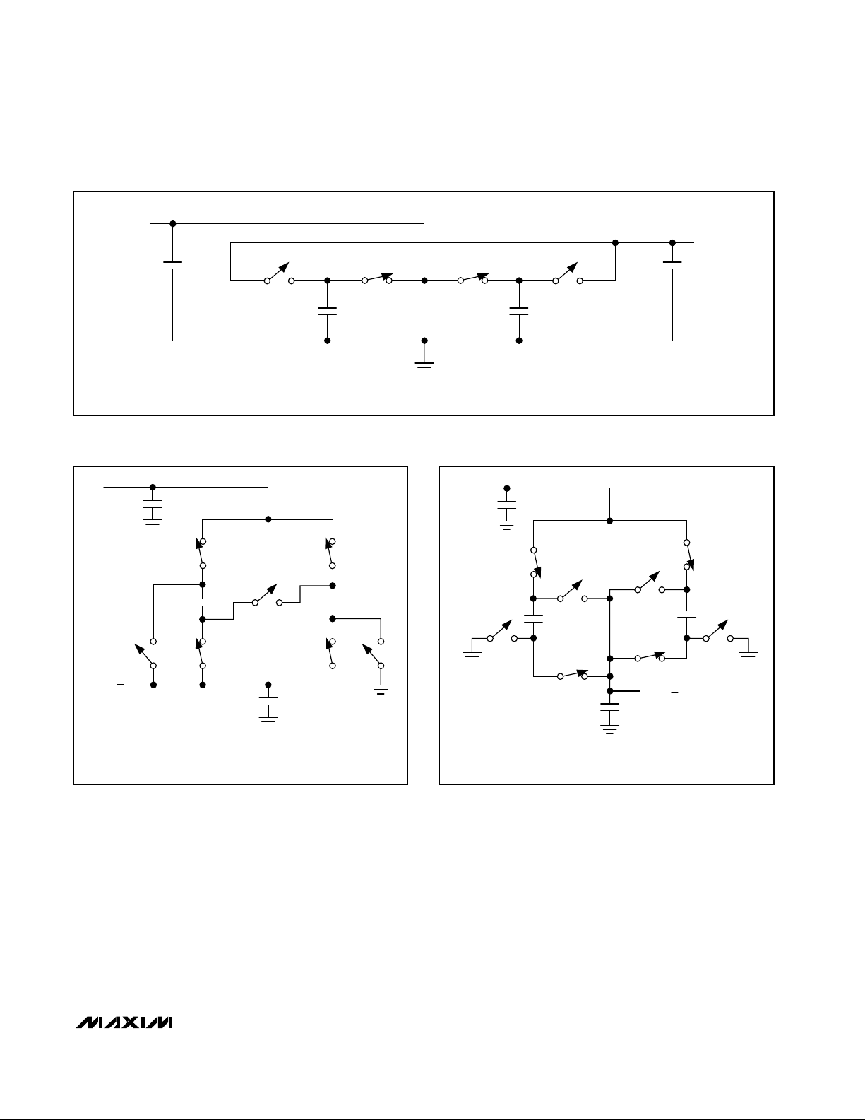
Charge-Pump Configurations
Charge pumps work by passing energy through capacitors. They generally work in two phases. In the first phase,
the input source charges the flying capacitors. The input
capacitor helps reduce the source’s input impedance. In
the second phase, the switching capacitors transfer their
charge to the output as needed.
Figure 1 shows the 1:1 charge-pump configuration. C1
and C2 charge in parallel between IN and GND during
the first phase. In the second phase, C1 and C2 connect
in parallel between OUT and GND.
Figure 2 shows the 3:2 charge-pump configuration. C1
and C2 charge in parallel between IN and OUT during
the first phase. In the second phase, C1 and C2 connect
in series between OUT and GND.
Figure 3 shows the 2:1 charge-pump configuration. C1
and C2 charge in parallel between IN and OUT during
the first phase. In the second phase, C1 and C2 connect
in parallel between OUT and GND.
Pulse-Skipping PFM and Mode
Transitions
In the MAX1730, pulse-skipping PFM mode pauses the
oscillator when the output is in regulation. Using the 2:1
charge-pump configuration as an example, when the
output is set to half the input, the switching frequency is
near the oscillator frequency. However, for outputs below
half the input, switching pauses once the desired output
level is achieved. With no output current, the device
switches occasionally. With higher levels of current, the
switching frequency increases to supply the load.
50mA Regulated Step-Down Charge Pump
for 1.8V or 1.9V Logic
6 _______________________________________________________________________________________
Functional Diagram
FB
FB CONTROL
OUT
C1P
SHDN
VREF
+
OSCILLATOR
SHUTDOWN
GND
MAX1730
CONTROL LOGIC
DRIVERS
SWITCH ARRAY
IN
C1N
C2P
C2N
PGND
Page 7
To maximize efficiency, the MAX1730 automatically
switches between charge-pump configurations (Figures
1, 2, and 3). Efficiency is greatest when the IN/OUT voltage ratio is close to the voltage ratio of the selected
capacitor configuration and decreases for output voltages lower than the divider ratio. To choose between
configurations, the MAX1730 senses the input voltage
and the output voltage. The MAX1730 uses a control
scheme with hysteresis to prevent oscillation between
capacitor configurations.
Applications Information
Setting the Output Voltage
For an output voltage of 1.8V, connect FB to GND. For
an output voltage of 1.9V, connect FB to IN.
MAX1730
50mA Regulated Step-Down Charge Pump
for 1.8V or 1.9V Logic
_______________________________________________________________________________________ 7
Figure 1. 1:1 Capacitor Configuration
Figure 2. 3:2 Capacitor Configuration
Figure 3. 2:1 Capacitor Configuration
V
IN
C
IN
NOTE: SWITCH STATES SET FOR STAGE 1.
ALL SWITCHES REVERSE STATE FOR STAGE 2.
C1 C2
V
= V
OUT
IN
C
OUT
V
IN
C
IN
C1 C2
2
V
= V
OUT
IN
3
NOTE: SWITCH STATES SET FOR STAGE 1.
ALL SWITCHES REVERSE STATE FOR STAGE 2.
C
OUT
V
IN
C
IN
1
= V
2
C2
IN
C1
NOTE: SWITCH STATES SET FOR STAGE 1.
ALL SWITCHES REVERSE STATE FOR STAGE 2.
V
OUT
C
OUT
Page 8

MAX1730
50mA Regulated Step-Down Charge Pump
for 1.8V or 1.9V Logic
Maxim cannot assume responsibility for use of any circuitry other than circuitry entirely embodied in a Maxim product. No circuit patent licenses are
implied. Maxim reserves the right to change the circuitry and specifications without notice at any time.
8 _____________________Maxim Integrated Products, 120 San Gabriel Drive, Sunnyvale, CA 94086 408-737-7600
© 2000 Maxim Integrated Products Printed USA is a registered trademark of Maxim Integrated Products.
Shutdown
The MAX1730 features an active-low shutdown pin
(SHDN) to decrease supply current to below 5µA.
When in shutdown, the output disconnects from the
input and OUT goes to high impedance.
Capacitor Selection
The input capacitor provides the charge pump with a lowimpedance supply. For most applications, a 1µF ceramic
capacitor is adequate. Lower-value capacitors and those
with higher ESR may be inadequate for proper operation
and may result in lower output current capability and
higher output ripple.
To reduce the output voltage ripple, the value of the
output capacitor should exceed that of the flying
capacitors (C1 + C2) by 10:1 or more. Values for C1
and C2 between 0.22µF and 0.47µF are recommended
for most applications. Use ceramic capacitors to
increase maximum output current and improve efficiency.
Layout Considerations
The MAX1730’s high-frequency operation demands
careful layout. All components should be placed as
close to the IC as possible, with priority going to CIN,
C1, and C2. Traces should be kept short, wide, and as
straight as possible. Connect PGND and GND together
with a low-impedance ground plane.
Chip Information
TRANSISTOR COUNT: 2295
Package Information
10LUMAX.EPS
Note: The MAX1730 does not have an exposed pad.
 Loading...