

Page 1
General Description
The MAX1722/MAX1723/MAX1724 compact, high-efficiency, step-up DC-DC converters are available in tiny, 5pin thin SOT23 packages. They feature an extremely low
1.5µA quiescent supply current to ensure the highest possible light-load efficiency. Optimized for operation from
one to two alkaline or nickel-metal-hydride (NiMH) cells, or
a single Li+ cell, these devices are ideal for applications
where extremely low quiescent current and ultra-small size
are critical.
Built-in synchronous rectification significantly improves
efficiency and reduces size and cost by eliminating the
need for an external Schottky diode. All three devices feature a 0.5Ω N-channel power switch. The MAX1722/
MAX1724 also feature proprietary noise-reduction circuitry,
which suppresses electromagnetic interference (EMI)
caused by the inductor in many step-up applications. The
family offers different combinations of fixed or adjustable
outputs, shutdown, and EMI reduction (see Selector
Guide).
Applications
Features
♦ Up to 90% Efficiency
♦ No External Diode or FETs Needed
♦ 1.5µA Quiescent Supply Current
♦ 0.1µA Logic-Controlled Shutdown
♦ ±1% Output Voltage Accuracy
♦ Fixed Output Voltage (MAX1724) or Adjustable
Output Voltage (MAX1722/MAX1723)
♦ Up to 150mA Output Current
♦ 0.8V to 5.5V Input Voltage Range
♦ 0.91V Guaranteed Startup (MAX1722/MAX1724)
♦ Internal EMI Suppression (MAX1722/MAX1724)
♦ Thin SOT23-5 Package (1.1mm max Height)
MAX1722/MAX1723/MAX1724
1.5µA IQ, Step-Up DC-DC Converters
in Thin SOT23-5
________________________________________________________________ Maxim Integrated Products 1
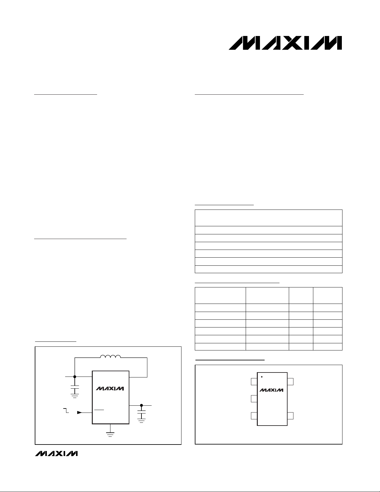
Typical Operating Circuit
19-1735; Rev 0; 7/01
Ordering Information
Selector Guide
Pagers
Remote Controls
Remote Wireless
Transmitters
Personal
Medical Devices
Digital Still Cameras
Single-Cell BatteryPowered Devices
Low-Power Hand-Held
Instruments
MP3 Players
Personal Digital
Assistants (PDA)
Pin Configurations are continued at end of data sheet.
PART
MAX1722EZK
MAX1723EZK
MAX1724EZK27 Fixed 2.7
Adjustable
Adjustable
OUTPUT (V)
SHDN
No
Yes
Yes
MAX1724EZK30
MAX1724EZK33
MAX1724EZK50 Fixed 5.0
Fixed 3.3
Fixed 3.0 Yes
Yes
Yes
LX
DAMPING
Yes
No
Yes
Yes
Yes
Yes
ADQK
ADQJ
ADQI
ADQH
ADQG
ADQF
TOP
MARK
5 SOT23
5 SOT23
5 SOT23-40°C to +85°C
-40°C to +85°C
-40°C to +85°C
MAX1724EZK50-T
MAX1724EZK33-T
MAX1724EZK30-T
5 SOT23
5 SOT23
5 SOT23
PINPACKAGE
TEMP. RANGE
-40°C to +85°C
-40°C to +85°C
-40°C to +85°C
MAX1724EZK27-T
MAX1723EZK-T
MAX1722EZK-T
PART
For pricing, delivery, and ordering information, please contact Maxim/Dallas Direct! at
1-888-629-4642, or visit Maxim’s website at www.maxim-ic.com.
Pin Configurations
10µH
IN
0.8V TO 5.5V
BATT
LX
TOP VIEW
15LXBATT
MAX1724
ON
OFF
SHDN
OUT
GND
OUT
3.3V AT
UP TO 150mA
GND
MAX1722
2
34
THIN SOT23-5
OUTFB
Page 2
MAX1722/MAX1723/MAX1724
1.5µA IQ, Step-Up DC-DC Converters
in Thin SOT23-5
2 _______________________________________________________________________________________
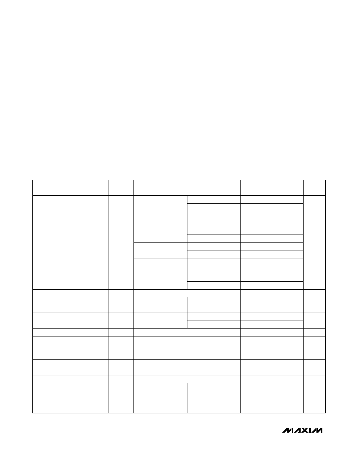
ABSOLUTE MAXIMUM RATINGS
ELECTRICAL CHARACTERISTICS
(V
BATT
= 1.2V, V
OUT
= 3.3V (MAX1722/MAX1723), V
OUT
= V
OUT(NOM)
(MAX1724), SHDN = OUT, RL= ∞, TA= 0°C to +85°C,
unless otherwise noted. Typical values are at T
A
= +25°C.) (Note 1)
Stresses beyond those listed under “Absolute Maximum Ratings” may cause permanent damage to the device. These are stress ratings only, and functional
operation of the device at these or any other conditions beyond those indicated in the operational sections of the specifications is not implied. Exposure to
absolute maximum rating conditions for extended periods may affect device reliability.
OUT, SHDN, BATT, LX to GND ................................-0.3V to +6V
FB to GND ................................................-0.3V to (V
OUT
+ 0.3V)
OUT, LX Current.......................................................................1A
Continuous Power Dissipation (TA= +70°C)
5-Pin Thin SOT23 (derate 7.1mW/°C above +70°C)...571mW
Operating Temperature Range ...........................-40°C to +85°C
Junction Temperature......................................................+150°C
Storage Temperature Range .............................-65°C to +150°C
Lead Temperature (soldering, 10s) ................................ +300°C
TA= +85°C
TA= +25°C
TA= 0°C to +85°C
TA= +25°C
TA= 0°C to +85°C
TA= +25°C
TA= 0°C to +85°C
TA= +25°C
TA= 0°C to +85°C
TA= +25°C
TA= 0°C to +85°C
TA= +25°C
MAX1723 (Note 2)
MAX1722/MAX1724
Shutdown Current into OUT
0.1
µA
Quiescent Current into OUT
1.5 3.6
µA
Quiescent Current into BATT
0.01
µA
MAX1723/MAX1724
(Notes 3, 4)
(Notes 3, 4)
MAX1722/MAX1724
(Note 4)
PARAMETER SYMBOL
MIN TYP MAX
UNITS
2.633 2.767
Output Voltage V
OUT
2.673 2.7 2.727
V
0.87 1.2
Minimum Startup Input Voltage
0.83 0.91
V
2.970 3.0 3.030
2.925 3.075
3.267 3.3 3.333
3.218 3.383
Operating Input Voltage
Minimum Input Voltage
0.8
V
V
IN
0.91 5.5
V
1.2 5.5
4.950 5.0 5.050
4.875 5.125
Output Voltage Range V
OUT
2 5.5
V
Feedback Voltage V
FB
1.223 1.235 1.247
V
1.210 1.260
Feedback Bias Current I
FB
1.5 20
nA
2.2
N-Channel On-Resistance R
DS(ON)
0.5 1.0
Ω
P-Channel On-Resistance R
DS(ON)
1.0 2.0
Ω
N-Channel Switch Current Limit I
LIM
400 500 600
mA
Switch Maximum On-Time t
ON
3.5 5 6.5
µs
Synchronous Rectifier ZeroCrossing Current
52035
mA
CONDITIONS
MAX1724EZK50
MAX1724EZK27
TA= +25°C,
RL= 3kΩ
MAX1724EZK30
MAX1722/MAX1723
MAX1722/MAX1723
MAX1724EZK33
MAX1722/MAX1723
MAX1722/MAX1724
V
OUT
forced to 3.3V
TA= +25°C
V
OUT
forced to 3.3V
V
OUT
forced to 3.3V
V
OUT
forced to 3.3V
MAX1722/MAX1724
MAX1723 (Note 2)
TA= +85°C
TA= +25°C
0.01 0.5
TA= +85°C
TA= +25°C
0.001 0.5
Page 3
MAX1722/MAX1723/MAX1724
1.5µA IQ, Step-Up DC-DC Converters
in Thin SOT23-5
_______________________________________________________________________________________ 3
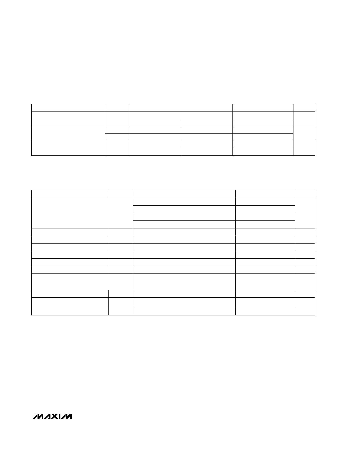
ELECTRICAL CHARACTERISTICS (continued)
(V
BATT
= 1.2V, V
OUT
= 3.3V (MAX1722/MAX1723), V
OUT
= V
OUT(NOM)
(MAX1724), SHDN = OUT, RL= ∞, TA= 0°C to +85°C,
unless otherwise noted. Typical values are at T
A
= +25°C.) (Note 1)
Note 1: Limits are 100% production tested at T
A
= +25°C. Limits over the operating temperature range are guaranteed by design.
Note 2: Guaranteed with the addition of a Schottky MBR0520L external diode between LX and OUT when using the MAX1723
with only one cell, and assumes a 0.3V voltage drop across the Schottky diode (see Figure 3).
Note 3: Supply current is measured with an ammeter between the output and OUT pin. This current correlates directly with actual
battery supply current, but is reduced in value according to the step-up ratio and efficiency.
Note 4: V
OUT
forced to the following conditions to inhibit switching: V
OUT
= 1.05 ✕V
OUT(NOM)
(MAX1724), V
OUT
= 3.465V
(MAX1722/MAX1723).
V
IL
MAX1723/MAX1724
TA= +85°C
TA= +25°C
TA= +85°C
TA= +25°C
0.001 0.5
SHDN Voltage Threshold
V
IH
500 800
mV
Shutdown Current into BATT
0.01
µA
SHDN Input Bias Current
7
nA
MAX1724 (Note 4)
MAX1723/MAX1724,
V
SHDN
= 5.5V
PARAMETER SYMBOL
MIN TYP MAX
UNITSCONDITIONS
MAX1723/MAX1724
75 400
2 100
ELECTRICAL CHARACTERISTICS
(V
BATT
= 1.2V, V
OUT
= 3.3V (MAX1722/MAX1723), V
OUT
= V
OUT(NOM)
(MAX1724), SHDN = OUT, RL= ∞, TA= -40°C to +85°C,
unless otherwise noted.) (Note 1)
PARAMETER SYMBOL CONDITIONS MIN TYP MAX UNITS
O utp ut V ol tag eV
O utp ut V ol tag e Rang eV
Feedback Voltage V
N-Channel On-Resistance
P-Channel On-Resistance
N-Channel Switch Current Limit I
Switch Maximum On-Time t
Synchronous Rectifier ZeroCrossing Current
Quiescent Current into OUT (Notes 3,4) 3.6 µA
SHDN Voltage Threshold
OUT
OUT
FB
R
DS(ON)
R
DS(ON)
LIM
ON
V
V
MAX1724EZK27 2.633 2.767
MAX1724EZK30 2.925 3.075
MAX1724EZK33 3.218 3.383
MAX1724EZK50 4.875 5.125
MAX1722/MAX1723 2 5.5 V
MAX1722/MAX1723 1.200 1.270 V
V
OUT
V
OUT
V
OUT
V
OUT
MAX1723/MAX1724 75
IL
MAX1723/MAX1724 800
IH
forced to 3.3V 1.0 Ω
forced to 3.3V 2.0 Ω
forced to 3.3V 400 620 mA
forced to 3.3V 5 35 mA
3.5 6.5 µs
V
mV
Page 4
MAX1722/MAX1723/MAX1724
1.5µA IQ, Step-Up DC-DC Converters
in Thin SOT23-5
4 _______________________________________________________________________________________
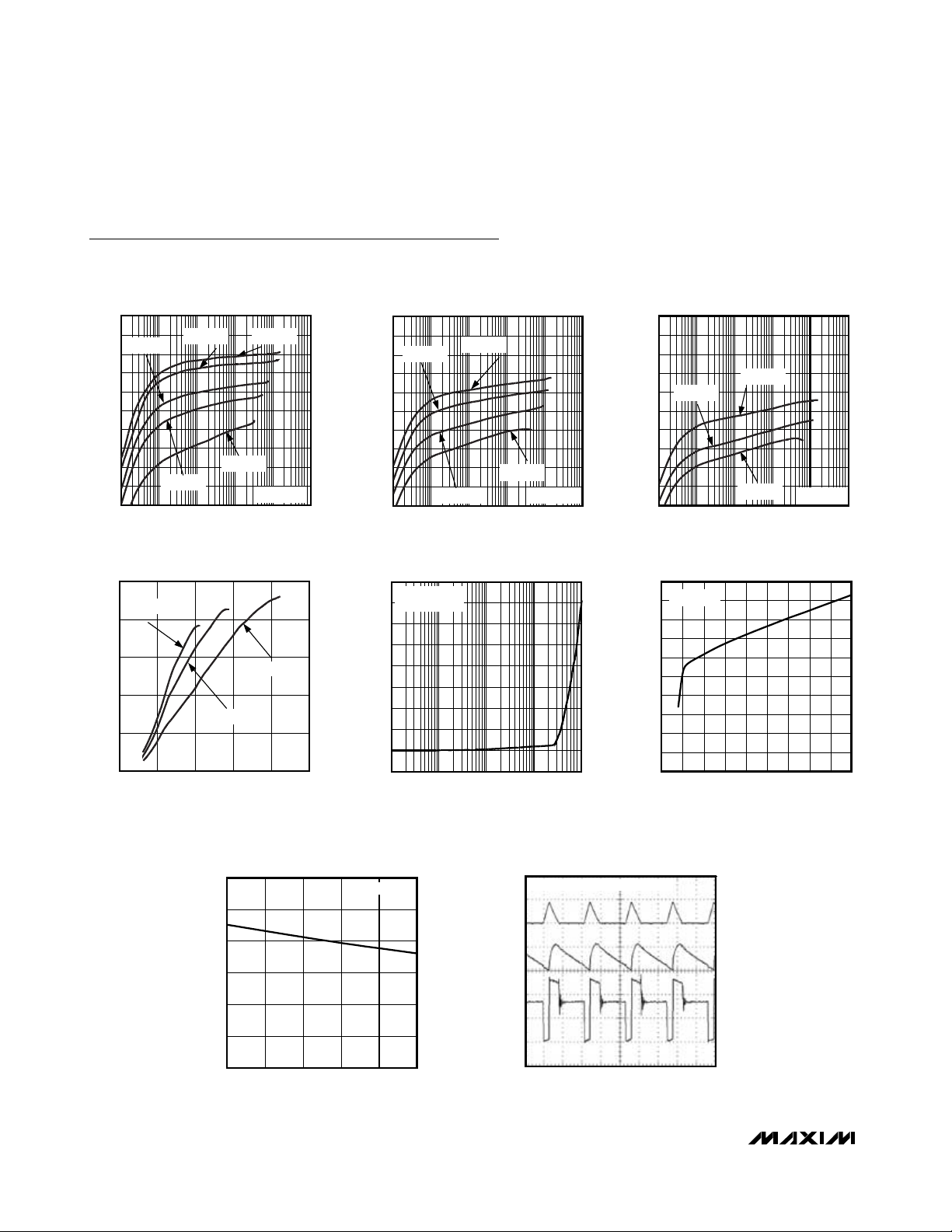
Typical Operating Characteristics
(Figure 3 (MAX1723), Figure 7 (MAX1722), Figure 8 (MAX1724), V
BATT
= VIN= 1.5V, L = 10µH, CIN= 10µF, C
OUT
= 10µF, TA= +25°C,
unless otherwise noted.)
0
40
120
80
160
200
021345
MAXIMUM OUTPUT CURRENT
vs. INPUT VOLTAGE
MAX1722 toc04
INPUT VOLTAGE (V)
I
OUT(MAX)
(mA)
V
OUT
= 2.5V
V
OUT
= 5.0V
V
OUT
= 3.3V
10 100
0.8
1.0
1.2
1.4
1.6
2.0
1.8
2.2
2.4
0.01 0.1 1
STARTUP VOLTAGE
vs. LOAD CURRENT
MAX1722 toc05
LOAD CURRENT (mA)
STARTUP VOLTAGE (V)
0.6
RESISTIVE LOAD
V
OUT
= 5.0V
0
0.4
0.2
0.8
0.6
1.2
1.0
1.4
1.8
1.6
2.0
1.0 2.0 2.5 3.01.5 3.5 4.0 4.5 5.0 5.5
MAX1722 toc06
QUIESCENT CURRENT (µA)
OUTPUT VOLTAGE (V)
QUIESCENT CURRENT INTO OUT
vs. OUTPUT VOLTAGE
NO LOAD
100
0.01 0.1 1 10 100 1000
EFFICIENCY vs. LOAD CURRENT
(V
OUT
= 5.0V)
MAX1722 toc01
LOAD CURRENT (mA)
EFFICIENCY (%)
60
80
50
70
90
VIN = 2.0V
VIN = 3.3V VIN = 4.0V
VIN = 1.5V
VIN = 1.0V
L = DO1606
100
0.01 0.1 1 10 100 1000
EFFICIENCY vs. LOAD CURRENT
(V
OUT
= 3.3V)
MAX1722 toc02
LOAD CURRENT (mA)
EFFICIENCY (%)
60
80
50
70
90
VIN = 2.0V
VIN = 2.5V
VIN = 1.5V
VIN = 1.0V
L = DO1606
100
0.01 0.1 1 10 100 1000
EFFICIENCY vs. LOAD CURRENT
(V
OUT
= 2.5V)
MAX1722 toc03
LOAD CURRENT (mA)
EFFICIENCY (%)
60
80
50
70
90
VIN = 1.5V
VIN = 2.0V
VIN = 1.0V
L = DO1606
0
0.4
0.2
0.8
0.6
1.0
1.2
-40 85
STARTUP VOLTAGE vs.
TEMPERATURE
MAX1722 toc07
TEMPERATURE (°C)
STARTUP VOLTAGE (V)
10-15 35 60
NO LOAD
1µs/div
I
LX
500mA/div
V
OUT
50mV/div
V
LX
2V/div
SWITCHING WAVEFORMS
MAX1722 toc08
I
OUT
= 50mA, V
OUT
= 5.0V, VIN = 3.3V
Page 5

MAX1722/MAX1723/MAX1724
1.5µA IQ, Step-Up DC-DC Converters
in Thin SOT23-5
_______________________________________________________________________________________ 5
Pin Description
1ms/div
V
SHDN
1V/div
5V
0
0
2V
SHUTDOWN RESPONSE
MAX1722 toc10
VIN = 3.3V, V
OUT
= 5.0V, R
OUT
= 100
Ω
V
OUT
2V/div
0
0.1
0.2
0.3
0.4
0.5
0.6
0.7
0.8
-40 -15 10 35 60 85
SHUTDOWN INPUT THRESHOLD
vs. TEMPERATURE
MAX1722 toc11
TEMPERATURE (°C)
SHUTDOWN THRESHOLD (mV)
RISING EDGE
FALLING EDGE
Typical Operating Characteristics (continued)
(Figure 3 (MAX1723), Figure 7 (MAX1722), Figure 8 (MAX1724), V
BATT
= VIN= 1.5V, L = 10µH, CIN= 10µF, C
OUT
= 10µF, TA= +25°C,
unless otherwise noted.)
MAX1724MAX1722
MAX1723
OUT
LX
FB
GND
SHDN
BATT
NAME
4
5
—
2
3
1
Power Output. OUT also provides bootstrap power to the IC.44
Internal N-channel MOSFET Switch Drain and P-Channel Synchronous
Rectifier Drain
55
Feedback Input to Set Output Voltage. Use a resistor-divider network to
adjust the output voltage. See Setting the Output Voltage section.
33
Ground22
PIN
Shutdown Input. Drive high for normal operation. Drive low for shutdown.1—
Battery Input and Damping Switch Connection—1
FUNCTION
200µs/div
A
A: V
OUT
, 50mV/div
B: I
OUT
, 20mA/div
B
LOAD-TRANSIENT RESPONSE
MAX1722 toc09
3.3V
50mA
0
Page 6

MAX1722/MAX1723/MAX1724
1.5µA IQ, Step-Up DC-DC Converters
in Thin SOT23-5
6 _______________________________________________________________________________________
Detailed Description
The MAX1722/MAX1723/MAX1724 compact, high-efficiency, step-up DC-DC converters are guaranteed to
start up with voltages as low as 0.91V and operate with
an input voltage down to 0.8V. Consuming only 1.5µA of
quiescent current, these devices include a built-in synchronous rectifier that reduces cost by eliminating the
need for an external diode and improves overall efficiency by minimizing losses in the circuit (see Synchronous
Rectification section). The MAX1722/MAX1724 feature a
clamp circuit that reduces EMI due to inductor ringing.
The MAX1723/MAX1724 feature an active-low shutdown
that reduces quiescent supply current to 0.1µA. The
MAX1722/MAX1723 have an adjustable output voltage,
while the MAX1724 is available with four fixed-output
voltage options (see Selector Guide). Figure 1 is the
MAX1723 simplified functional diagram and Figure 2 is
the MAX1724 simplified functional diagram.
PFM Control Scheme
A forced discontinuous, current-limited, pulse-frequencymodulation (PFM) control scheme is a key feature of the
MAX1722/MAX1723/MAX1724. This scheme provides
ultra-low quiescent current and high efficiency over a
wide output current range. There is no oscillator; the
inductor current is limited by the 0.5A N-channel current limit or by the 5µs switch maximum on-time.
Following each on cycle, the inductor current must
ramp to zero before another cycle may start. When the
error comparator senses that the output has fallen
below the regulation threshold, another cycle begins.
Synchronous Rectification
The internal synchronous rectifier eliminates the need
for an external Schottky diode, thus reducing cost and
board space. While the inductor discharges, the Pchannel MOSFET turns on and shunts the MOSFET
body diode. As a result, the rectifier voltage drop is significantly reduced, improving efficiency without the
addition of external components.
Low-Voltage Startup Circuit
The MAX1722/MAX1723/MAX1724 contain a low-voltage startup circuit to control DC-DC operation until the
output voltage exceeds 1.5V (typ). The minimum start-
Figure 1. MAX1723 Simplified Functional Diagram
OUT
MAX1723
STARTUP
CIRCUITRY
SHDN
CONTROL
LOGIC
FB
ERROR
COMPARATOR
1.235V REFERENCE
DRIVER
CURRENT
LIMIT
ZEROCROSSING
DETECTOR
P
LX
N
GND
Page 7

MAX1722/MAX1723/MAX1724
1.5µA IQ, Step-Up DC-DC Converters
in Thin SOT23-5
_______________________________________________________________________________________ 7
up voltage is a function of load current (see Typical
Operating Characteristics). This circuit is powered from
the BATT pin for the MAX1722/MAX1724, guaranteeing
startup at input voltages as low as 0.91V. The MAX1723
lacks a BATT pin; therefore, this circuit is powered
through the OUT pin. Adding a Schottky diode in parallel with the P-channel synchronous rectifier allows for
startup voltages as low as 1.2V for the MAX1723
(Figure 3). The external Schottky diode is not needed
for input voltages greater than 1.8V. Once started, the
output maintains the load as the battery voltage
decreases below the startup voltage.
Shutdown (MAX1723/MAX1724)
The MAX1723/MAX1724 enter shutdown when the
SHDN pin is driven low. During shutdown, the body
diode of the P-channel MOSFET allows current to flow
from the battery to the output. V
OUT
falls to approximately VIN- 0.6V and LX remains high impedance.
Shutdown can be pulled as high as 6V, regardless of
the voltage at BATT or OUT. For normal operation, connect SHDN to the input.
BATT
Figure 2. MAX1724 Simplified Functional Diagram
Figure 3. MAX1723 Single-Cell Operation
SHDN
DAMPING
SWITCH
OUT
MAX1724
ZERO-
DRIVER
CURRENT
LIMIT
CROSSING
DETECTOR
P
LX
N
STARTUP
CIRCUITRY
R
2
CONTROL
LOGIC
ERROR
COMPARATOR
R
1
1.235V REFERENCE
µH
1.2V
TO V
10µF
OUT
10
SHDN
OUT
MAX1723
GND FB
R2
2.37MΩ
R1
1.24MΩ
D1
V
= 3.6V
OUT
10µF
LX
GND
Page 8

MAX1722/MAX1723/MAX1724
1.5µA IQ, Step-Up DC-DC Converters
in Thin SOT23-5
8 _______________________________________________________________________________________
BATT/Damping Switch
(MAX1722/MAX1724)
The MAX1722/MAX1724 include an internal damping
switch (Figure 4) to minimize ringing at LX and reduce
EMI. When the energy in the inductor is insufficient to
supply current to the output, the capacitance and
inductance at LX form a resonant circuit that causes
ringing. The damping switch supplies a path to quickly
dissipate this energy, suppressing the ringing at LX.
This does not reduce the output ripple, but does
reduce EMI with minimal impact on efficiency. Figures
5 and 6 show the LX node voltage waveform without
and with the damping switch, respectively.
Design Procedure
Setting the Output Voltage
(MAX1722/MAX1723)
The output voltage can be adjusted from 2V to 5.5V
using external resistors R1 and R2 (Figure 7). Since FB
leakage is 20nA (max), select feedback resistor R1 in
the 100kΩ to 1MΩ range. Calculate R2 as follows:
where VFB= 1.235V.
Figure 6. LX Ringing With Damping Switch (MAX1722/MAX1724)
Figure 5. LX Ringing Without Damping Switch (MAX1723)
Figure 4. Simplified Diagram of Damping Switch
V
OUT
V
IN
OUT
MAX1722
MAX1724
PDRV
P
BATT
N
GND
DAMPING
SWITCH
TIMING
CIRCUIT
DAMP
NDRV
1V/div
1µs/div
LX
1V/div
1µs/div
V
RR
21 1 =−
OUT
V
FB
Page 9

MAX1722/MAX1723/MAX1724
1.5µA IQ, Step-Up DC-DC Converters
in Thin SOT23-5
_______________________________________________________________________________________ 9
Inductor Selection
The control scheme of the MAX1722/MAX1723/
MAX1724 permits flexibility in choosing an inductor. A
10µH inductor value performs well in most applications.
Smaller inductance values typically offer smaller physical size for a given series resistance, allowing the
smallest overall circuit dimensions. Circuits using larger
inductance values may start up at lower battery voltages, provide higher efficiency, and exhibit less ripple,
but they may reduce the maximum output current. This
occurs when the inductance is sufficiently large to prevent the maximum current limit (I
LIM
) from being
reached before the maximum on-time (t
ON(MAX)
)
expires.
For maximum output current, choose the inductor value
so that the controller reaches the current-limit before
the maximum on-time is triggered:
where the maximum on-time is typically 5µs, and the
current limit (I
LIM
) is typically 500mA (see Electrical
Characteristics table).
For larger inductor values, determine the peak inductor
current (I
PEAK)
by:
The inductor’s incremental saturation current rating should
be greater than the peak switching current. However, it is
generally acceptable to bias the inductor into saturation
by as much as 20%, although this will slightly reduce efficiency. Table 1 lists suggested inductors and suppliers.
Maximum Output Current
The maximum output current depends on the peak inductor current, the input voltage, the output voltage, and the
overall efficiency (η):
Figure 8. MAX1724 Standard Application Circuit
Table 1. Suggested Inductors and
Suppliers
Figure 7. Adjustable Output Circuit
INPUT
OUT
0.8V TO V
10µF
BATT
10µH
MAX1722
GND
OUT
LX
FB
OUTPUT
2V TO 5.5V
R2
10µF
R1
MANUFACTURER INDUCTOR
Coilcraft
Murata LQH4C Series
Sumida
DO1608 Series
DO1606 Series
CDRH4D18 Series
CR32 Series
CMD4D06 Series
PHONE
WEBSITE
847-639-2361
www.coilcraft.com
770-436-1300
www.murata.com
847-545-6700
www.sumida.com
Vt
BATT ON MAX
L
<
I
LIM
()
10µF
0.8V TO V
C1
INPUT
ON
OUT
OFF
I
PEAK
Vt
BATT ON MAX
=
10µH
BATT
MAX1724
SHDN
GND
()
L
LX
OUT
OUTPUT
V
OUT (NOM)
C2
10µF
Sumitomo/
Daidoo Electronics
Toko
CXLD140 Series
3DF Type
D412F Type
+81 (06) 6355-5733
www.daidoo.co.jp
847-297-0070
www.toko.com
II
OUT MAX PEAK
()
1
=
2
V
BATT
V
OUT
η
Page 10

For most applications, the peak inductor current equals
the current limit. However, for applications using large
inductor values or low input voltages, the maximum ontime limits the peak inductor current (see Inductor
Selection section).
Capacitor Selection
Choose input and output capacitors to supply the input
and output peak currents with acceptable voltage ripple. The input filter capacitor (CIN) reduces peak currents drawn from the battery and improves efficiency.
Low equivalent series resistance (ESR) capacitors are
recommended. Ceramic capacitors have the lowest
ESR, but low ESR tantalum or polymer capacitors offer
a good balance between cost and performance.
Output voltage ripple has two components: variations
in the charge stored in the output capacitor with each
LX pulse, and the voltage drop across the capacitor’s
ESR caused by the current into and out of the capacitor:
where I
PEAK
is the peak inductor current (see Inductor
Selection section). For ceramic capacitors, the output
voltage ripple is typically dominated by V
RIPPLE(C)
. For
example, a 10µF ceramic capacitor and a 10µH inductor typically provide 75mV of output ripple when stepping up from 3.3V to 5V at 50mA. Low input-to-output
voltage differences (i.e. two cells to 3.3V) require higher output capacitor values.
Capacitance and ESR variation of temperature should
be considered for best performance in applications
with wide operating temperature ranges. Table 2 lists
suggested capacitors and suppliers.
PC Board Layout Considerations
Careful PC board layout is important for minimizing
ground bounce and noise. Keep the IC’s GND pin and
the ground leads of the input and output capacitors
less than 0.2in (5mm) apart using a ground plane. In
addition, keep all connections to FB
(MAX1722/MAX1723 only) and LX as short as possible.
MAX1722/MAX1723/MAX1724
1.5µA IQ, Step-Up DC-DC Converters
in Thin SOT23-5
10 ______________________________________________________________________________________
Table 2. Suggested Surface-Mount Capacitors and Manufacturers (C1 and C2)
Chip Information
TRANSISTOR COUNT: 863
MANUFACTURER
AVX
Sanyo 33µF to 330µF TPC Polymer Series
Taiyo Yuden 33µF to 330µF X5R/X7R Ceramic
TDK 1µF to 10µF X7R Ceramic
Vishay Sprague 10µF to 330µF
CAPACITOR
VALUE
1µF to 10µF X7R Ceramic
10µF to 330µF
1µF to 22µF X5R/X7R Ceramic
10µF to 330µF T494 Tantalum SeriesKemet
68µF to 330µF T520 Tantalum Series
DESCRIPTION
TAJ Tantalum Series
TPS Tantalum Series
594D Tantalum Series
595D Tantalum Series
VV V
V
V
=+
RIPPLE RIPPLE C RIPPLE ESR
RIPPLE ESR
RIPPLE C
() ( )
≈
I R
() ( )
()
PEAK ESR COUT
1
≈
2
VVC
()
L
-
OUT BATT OUT
I-
()
PEAK OUT
2
2
I
PHONE
WEBSITE
843-448-9411
www.avxcorp.com
864-963-6300
www.kemet.com
408-749-9714
www.secc.co.jp
800-368-2496
www.t-yuden.org
847-803-6100
www.tdk.com
203-452-5664
www.vishay.com
Page 11

MAX1722/MAX1723/MAX1724
1.5µA IQ, Step-Up DC-DC Converters
in Thin SOT23-5
______________________________________________________________________________________ 11
Package Information
Pin Configurations (continued)
TOP VIEW
15LXSHDN
MAX1723
2
GND
34
THIN SOT23-5
OUTFB
15LXBATT
MAX1724
2
GND
34
SHDN
THIN SOT23-5
OUT
THIN SOT23.EPS
Page 12

MAX1722/MAX1723/MAX1724
1.5µA IQ, Step-Up DC-DC Converters
in Thin SOT23-5
Maxim cannot assume responsibility for use of any circuitry other than circuitry entirely embodied in a Maxim product. No circuit patent licenses are
implied. Maxim reserves the right to change the circuitry and specifications without notice at any time.
12 ____________________Maxim Integrated Products, 120 San Gabriel Drive, Sunnyvale, CA 94086 408-737-7600
© 2001 Maxim Integrated Products Printed USA is a registered trademark of Maxim Integrated Products.
Package Information (continued)
 Loading...