

Page 1
19-5241; Rev 0; 4/10
EVALUATION KIT
AVAILABLE
Internal-Switch Boost Regulator with Integrated
7-Channel Scan Driver, Op Amp, and LDO
General Description
The MAX17117 includes a high-performance step-up
regulator, a 350mA low-dropout (LDO) linear regulator,
a high-speed operational amplifier, and a high-voltage
level-shifting scan driver with gate-shading control. The
device is optimized for thin-film transistor (TFT) liquidcrystal display (LCD) applications.
The step-up DC-DC converter provides the regulated
supply voltage for panel source-driver ICs. The high
1.2MHz switching frequency allows the use of ultra-small
inductors and ceramic capacitors. The current-mode
control architecture provides a fast-transient response to
pulsed loads typical of source driver loads. The step-up
regulator features an adjustable soft-start and an adjustable cycle-by-cycle current limit.
The high-current operational amplifier is designed to
drive the LCD backplane (VCOM). The amplifier features
high output current (Q200mA typ), fast slew rate (40V/Fs
typ), wide bandwidth (16MHz typ), and rail-to-rail inputs
and outputs.
The low-voltage LDO linear regulator has an integrated
0.8I pass element and can provide at least 350mA. The
output voltage is accurate within Q1%.
The high-voltage, level-shifting scan driver with gateshading control is designed to drive the TFT panel gate
drivers. Its seven outputs swing 40V (maximum) between
+35V (maximum) and -15V (minimum) and can swiftly
drive capacitive loads.
The MAX17117 is available in a 32-pin, 5mm x 5mm, thin
QFN package with a maximum thickness of 0.8mm for
thin LCD panels.
Ordering Information
PART TEMP RANGE PIN-PACKAGE
MAX17117ETJ+ -40NC to +85NC 32 TQFN-EP*
+Denotes a lead(Pb)-free/RoHS-compliant package.
*EP = Exposed pad.
Applications
Notebook Computer Displays
Features
S 2.3V to 5.5V IN Supply-Voltage Range
S 1.2MHz Current-Mode Step-Up Regulator
Fast-Transient Response
High-Accuracy Reference (1%)
Integrated 16V, 2A, 200mI MOSFET
High Efficiency (> 85%)
Adjustable Cycle-by-Cycle Current Limit
S High-Performance Operational Amplifier
200mA Output Short-Circuit Current
40V/µs Slew Rate
16MHz, -3dB Bandwidth
Low-Dropout Linear Regulator
High-Accuracy Output Voltage (1.0%)
S High-Voltage Drivers with Scan Logic
+35V to -15V Outputs
40V Maximum Voltage Swing
Gate-Shading Control
S Thermal-Overload Protection
S 32-Pin, 5mm x 5mm, Thin QFN Package
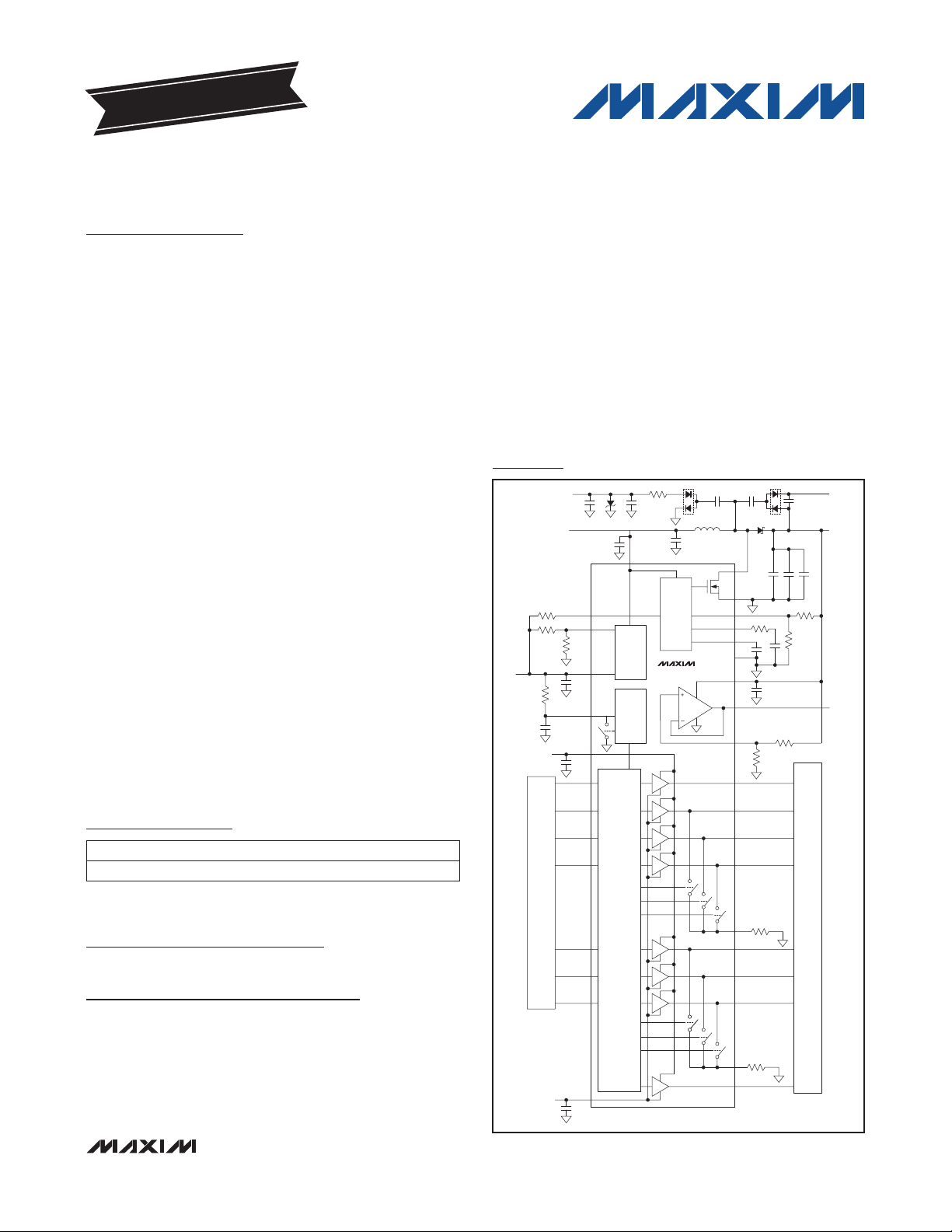
Simplified Operating Circuit
PANEL
V
GHON
V
MAIN
TO VCOM
BACKPLANE
V
VGL
V
IN
IN
LINEAR
GATE-
TIMING
SETUP
CONTROLLER
MAX17117
OP
ENA
LDOADJ
REGULATOR
V
SYSTEM
LDOO
DTS
SHADING
CONTROL
GHON
GHON
ST
CK1
CK3
CK5
SCAN DRIVER AND
GATE-SHADING
CONTROL LOGIC
CK2
CK4
CK6
VGL
V
VGL
V
LOGIC
LX
PGND
FB
COMP
SS
AGND
(EP)
OPAS
OUT
POS
STH
CKH1
CKH3
CKH5
S1
S3
S5
RO
CKH2
CKH4
CKH6
S2
S4
S6
RE
VGLC
MAX17117
_______________________________________________________________ Maxim Integrated Products 1
For pricing, delivery, and ordering information, please contact Maxim Direct at 1-888-629-4642,
or visit Maxim’s website at www.maxim-ic.com.
Page 2
Internal-Switch Boost Regulator with Integrated
7-Channel Scan Driver, Op Amp, and LDO
ABSOLUTE MAXIMUM RATINGS
IN, ENA, FB, COMP, SS, DTS, LDOADJ, ST,
CK1–CK6, LDOO to AGND ...............................-0.3V to +7.5V
PGND to AGND .................................................... -0.3V to +0.3V
LX, OPAS to PGND ...............................................-0.3V to +18V
GHON to PGND ....................................................-0.3V to +45V
VGL to PGND ....................................................... -20V to +0.3V
GHON to VGL .................................................................... +45V
STH, CKH1–CKH6, VGLC, RO,
RE to VGL .........................................-0.3V to (V
MAX17117
OUT, POS to PGND ..............................-0.3V to (V
Stresses beyond those listed under “Absolute Maximum Ratings” may cause permanent damage to the device. These are stress ratings only, and functional
operation of the device at these or any other conditions beyond those indicated in the operational sections of the specifications is not implied. Exposure to absolute
maximum rating conditions for extended periods may affect device reliability.
GHON
OPAS
+ 0.3V)
+ 0.3V)
ELECTRICAL CHARACTERISTICS
(VIN = +3V, Circuit of Figure 1, V
noted. Typical values are at TA = +25NC.)
PARAMETER CONDITIONS MIN TYP MAX UNITS
IN Input Voltage Range 2.3 5.5 V
IN Undervoltage-Lockout
Threshold
IN Quiescent Current
IN Standby Current V
GHON Standby Current V
OPAS Standby Current V
Thermal Shutdown Temperature rising 145 170
STEP-UP REGULATOR
Output Voltage Range V
OPAS Overvoltage Threshold OPAS rising 16.5 17 18 V
Operating Frequency 1000 1200 1400 kHz
Oscillator Maximum Duty Cycle 91 94 97 %
FB Regulation Voltage No load 1.227 1.240 1.252 V
FB Fault-Trip Level Falling edge 1.05 1.10 1.15 V
Fault-Trigger Delay 160 ms
FB Load Regulation 0 < I
FB Line Regulation
FB Input-Bias Current
FB Transconductance
LX Current Limit
LX On-Resistance ILX = 1A 200 500
LX Input-Bias Current
Current-Sense Transresistance 0.10 0.20 0.30 V/A
Soft-Start Pullup Current 2 4 6
= +8.5V, V
OPAS
VIN rising, typical hysteresis = 150mV 1.80 2.00 2.20 V
VFB = 1.3V, LX not switching 1.0 2.5
VFB = 1.2V, LX switching 2.5 5
= V
ENA
ENA
ENA
VIN = 2.5V to 5.5V, TA = +25NC
VFB = 1.24V, TA = +25NC
DI
R
ENA
V
LX
VGL
= V
VGL
= V
VGL
< full load -0.2 %
LOAD
= Q2.5FA, FB = COMP
COMP
= 10kW, duty cycle = 60%
= 13.5V, TA = +25NC
= +24V, V
GHON
= 0V, VIN = 5.5V, V
= 0V, VIN = 5.5V, V
= 0V, VIN = 5.5V, V
GHON and VGL RMS Current Rating ..................................0.8A
VGLC, STH, and CKH1–CKH6 RMS Current Rating ...........0.8A
LX, PGND RMS Current Rating ............................................1.6A
Continuous Power Dissipation (TA = +70NC)
32-Pin TQFN (derate 24.9mW/NC above +70NC) .......1990mW
Operating Temperature Range .......................... -40NC to +85NC
Junction Temperature .....................................................+150NC
Storage Temperature Range ............................ -65NC to +160NC
Lead Temperature (soldering, 10s) ................................+300NC
Soldering Temperature (reflow) ......................................+260NC
= -6.2V, VST = VCK_ = 0V, TA = 0NC to +85NC, unless otherwise
VGL
= 4V 0.7 2 mA
GHON
= 4V 100 200
GHON
= 4V 20 50
GHON
IN
0.1 0.25 %/V
65 200 nA
75 160 280
1.6 2 2.4 A
10 20
15 V
mA
FA
FA
NC
FS
mI
FA
FA
2 ______________________________________________________________________________________
Page 3
Internal-Switch Boost Regulator with Integrated
7-Channel Scan Driver, Op Amp, and LDO
ELECTRICAL CHARACTERISTICS (continued)
(VIN = +3V, Circuit of Figure 1, V
noted. Typical values are at TA = +25NC.)
PARAMETER CONDITIONS MIN TYP MAX UNITS
VCOM BUFFER
OPAS Voltage Range 5 15 V
OPAS Supply Current V
OUT Voltage Swing High I
OUT Voltage Swing Low I
OUT Short-Circuit Current
POS Input-Bias Current
POS Input-Offset Voltage V
Gain-Bandwidth Product 8 MHz
-3dB Bandwidth
Slew Rate
HIGH-VOLTAGE SCAN DRIVER
GHON Voltage Range 12 35 V
VGL Voltage Range -15 -3 V
GHON-to-VGL Voltage Range V
GHON Supply Current CK1 through CK6 and ST low 350 550
VGL Supply Current CK1 through CK6 and ST low -500 -300
Output Impedance Low STH, CKH_, VGLC, I
Output Impedance High STH, CKH_, VGLC, I
Gate-Shading Switch Resistance
RO, RE Resistance Range 100
Propagation Delay from ST
Rising Edge to STH Rising Edge
Propagation Delay from ST
Falling Edge to STH Falling Edge
Propagation Delay from CK_
Rising Edge to CKH_ Rising
Edge
Propagation Delay from CK_
Falling Edge to CKH_ Falling
Edge
STH, VGLC, CKH_ Rise Time
STH, VGLC, CKH_ Fall Time
STH, CKH_ Operating Frequency
Range
= +8.5V, V
OPAS
= V
POS
OUT
OUT
OPAS
= 5mA
= 5mA 50 100 mV
Sourcing, short to V
Sinking, short to V
V
= V
POS
OUT
R
LOAD
OPAS
= V
OPAS
= 10kI, C
5V pulse applied to POS, OUT measured from 10% to
90%
- V
GHON
GHON
= +24V, V
= -6.2V, VST = VCK_ = 0V, TA = 0NC to +85NC, unless otherwise
VGL
/2, no load 0.8 1.2 mA
/2 - 1V 100 200
OPAS
/2 + 1V 100 200
OPAS
/2, TA = +25NC
V
OPAS
- 100
V
OPAS
- 50
-50 +50 nA
/2 -15 +15 mV
LOAD
= 10pF
16 MHz
10 40
VGL
= -20mA 80
OUT
= +20mA 80
OUT
CKH1, CKH3, CKH5, IRE = 10mA 100
CKH2, CKH4, CKH6, IRO = 10mA 100
C
= 100pF, R
LOAD
C
= 100pF, R
LOAD
C
= 100pF, R
LOAD
C
= 100pF, R
LOAD
C
= 5nF, R
LOAD
V
= -10V; measured from 10% to 90%
VGL
C
= 5nF, R
LOAD
V
= -10V; measured from 10% to 90%
VGL
C
= 5nF, R
LOAD
LOAD
LOAD
LOAD
LOAD
LOAD
LOAD
LOAD
= 0I; V
= 0I; V
= 0I
= 0I
= 0I
= 0I
= 0I
GHON
GHON
= 30V,
= 30V,
100 200 ns
100 200 ns
100 200 ns
100 200 ns
0.5 1
0.5 1
mV
mA
V/Fs
40 V
FA
FA
I
I
I
I
Fs
Fs
100 kHz
MAX17117
_______________________________________________________________________________________ 3
Page 4
Internal-Switch Boost Regulator with Integrated
7-Channel Scan Driver, Op Amp, and LDO
ELECTRICAL CHARACTERISTICS (continued)
(VIN = +3V, Circuit of Figure 1, V
noted. Typical values are at TA = +25NC.)
PARAMETER CONDITIONS MIN TYP MAX UNITS
GATE-SHADING TIMING CONTROL
Gate-Shading Detection
Threshold
Gate-Shading Detection Current V
MAX17117
DTS Switch Resistance V
DTS Rising Edge Threshold 1.215 1.240 1.265 V
DTS Falling Edge Threshold 100 150 mV
LDO
LDOO Output Voltage Range 1.8 V
Dropout Voltage VIN = 3.3V, V
LDOO Line Regulation VIN = 2.8V to 5.5V, V
LDOO Load Regulation V
LDOO Current Limit V
LDOADJ Feedback Voltage 1.227 1.240 1.252 V
LDOADJ Input-Bias Current
DIGITAL INPUTS
ST, CK_ Input High Level 1.8V < V
ST, CK_ Input Low Level 1.8V < V
ENA Input Logic-High Level
ENA Input Logic-Low Level
ENA Resistor Range 0 200
= +8.5V, V
OPAS
DTS falling 100 150 mV
= 0.5V 5 10 15 µA
DTS
= 1.3V, I
DTS
= 2.5V, I
LDOO
= 1.0V 0.4 0.62 0.8 A
LDOADJ
V
1.8V < V
V
1.8V < V
V
= 1.3V, TA = +25NC
LDOADJ
LDOO
LDOO
LDOO
> 3.0V 2.1 V
LDOO
LDOO
> 3.0V 0.8 V
LDOO
= +24V, V
GHON
= 1mA 10 50
DTS
= 1.1V, I
LDOADJ
LDOO
= 1mA to 300mA 0.2 0.5 %/V
LDOO
< 5.5V
< 5.5V
< 3.0V
< 3.0V
= -6.2V, VST = VCK_ = 0V, TA = 0NC to +85NC, unless otherwise
VGL
= 350mA 300 500 mV
LDOO
= 2.5V, I
= 100mA 0.1 0.3 %/V
LDOO
0.7 x
V
LDOO
0.7 x
V
LDOO
IN
100 200 nA
0.3 x
V
LDOO
0.3 x
V
LDOO
I
V
V
V
V
V
kI
ELECTRICAL CHARACTERISTICS
(VIN = +3V, Circuit of Figure 1, V
erwise noted.)
PARAMETER CONDITIONS MIN TYP MAX UNITS
IN Input Voltage Range 2.3 5.5 V
IN Undervoltage-Lockout
Threshold
IN Quiescent Current
IN Standby Current V
GHON Standby Current V
OPAS Standby Current V
Thermal Shutdown Temperature rising 145
4 ______________________________________________________________________________________
= +8.5V, V
OPAS
VIN rising, typical hysteresis = 150mV 1.80 2.20 V
VFB = 1.3V, LX not switching 2.5
VFB = 1.2V, LX switching 5
= V
ENA
ENA
ENA
= V
= V
VGL
VGL
VGL
= +24V, V
GHON
= 0V, VIN = 5.5V, V
= 0V, VIN = 5.5V, V
= 0V, VIN = 5.5V, V
VGL
= -6.2V, VST = V
= 4V 2 mA
GHON
= 4V 160
GHON
= 4V 50
GHON
= 0V, TA = -40NC to +85NC, unless oth-
CK_
mA
FA
FA
NC
Page 5
Internal-Switch Boost Regulator with Integrated
7-Channel Scan Driver, Op Amp, and LDO
ELECTRICAL CHARACTERISTICS (continued)
(VIN = +3V, Circuit of Figure 1, V
erwise noted.)
PARAMETER CONDITIONS MIN TYP MAX UNITS
STEP-UP REGULATOR
Output Voltage Range V
OPAS Overvoltage Threshold OPAS rising 16.5 18 V
Operating Frequency 1000 1400 kHz
Oscillator Maximum Duty Cycle 91 97 %
FB Regulation Voltage No load 1.227 1.252 V
FB Fault-Trip Level Falling edge 1.05 1.15 V
FB Line Regulation
FB Input-Bias Current
FB Transconductance
LX Current Limit VFB = 1.2V, duty cycle = 60% 1.6 2.4 A
LX On-Resistance ILX = 1A 500
LX Input-Bias Current
Current-Sense Transresistance 0.10 0.30 V/A
Soft-Start Pullup Current 2 6
VCOM BUFFER
OPAS Voltage Range 5 15 V
OPAS Supply Current V
OUT Voltage Swing High I
OUT Voltage Swing Low I
OUT Short-Circuit Current
POS Input-Bias Current
POS Input-Offset Voltage V
Slew Rate
HIGH-VOLTAGE SCAN DRIVER
GHON Voltage Range 12 35 V
VGL Voltage Range -15 -3 V
GHON-to-VGL Voltage Range V
GHON Supply Current CK1 through CK6 and ST low 550
VGL Supply Current CK1 through CK6 and ST low -500
Output Impedance Low STH, CKH_, VGLC, I
Output Impedance High STH, CKH_, VGLC, I
Gate-Shading Switch Resistance
RO, RE Resistance Range 100
Propagation Delay from ST
Rising Edge to STH Rising Edge
= +8.5V, V
OPAS
VIN = 2.5V to 5.5V, TA = +25NC
VFB = 1.3V, TA = +25NC
DI
= Q2.5FA, FB = COMP
COMP
V
= 13.5V, TA = +25NC
LX
= V
POS
OUT
OUT
Sourcing, short to V
Sinking, short to V
V
POS
OUT
5V pulse applied to POS, OUT measured from 10% to
90%
GHON
CKH1, CKH3, CKH5, IRE = 10mA 100
CKH2, CKH4, CKH6, IRO = 10mA 100
C
OPAS
= 5mA
= 5mA 100 mV
= V
OPAS
= V
OPAS
- V
VGL
= 100pF, R
LOAD
= +24V, V
GHON
/2, no load 1.2 mA
/2 - 1V 100
OPAS
/2 + 1V 100
OPAS
/2, TA = +25NC
/2 -15 +15 mV
= -20mA 80
OUT
= +20mA 80
OUT
= 0I
LOAD
= -6.2V, VST = V
VGL
= 0V, TA = -40NC to +85NC, unless oth-
CK_
IN
75 280
V
OPAS
- 100
-50 +50 nA
10
15 V
0.3 %/V
200 nA
FS
mI
20
40 V
200 ns
FA
FA
mV
mA
V/Fs
FA
FA
I
I
I
I
MAX17117
_______________________________________________________________________________________ 5
Page 6
Internal-Switch Boost Regulator with Integrated
7-Channel Scan Driver, Op Amp, and LDO
ELECTRICAL CHARACTERISTICS (continued)
(VIN = +3V, Circuit of Figure 1, V
erwise noted.)
PARAMETER CONDITIONS MIN TYP MAX UNITS
Propagation Delay from ST
Falling Edge to STH Falling Edge
Propagation Delay from CK_
Rising Edge to CKH_ Rising Edge
MAX17117
Propagation Delay from CK_
Falling Edge to CKH_ Falling
Edge
STH, VGLC, CKH_ Rise Time
STH, VGLC, CKH_ Fall Time
STH, CKH_ Operating Frequency
Range
GATE-SHADING TIMING CONTROL
Gate-Shutdown Detection
Threshold
Gate-Shutdown Detection Current V
DTS Switch Resistance V
DTS Rising Edge Threshold 1.210 1.265 V
DTS Falling Edge Threshold 150 mV
LDO
LDOO Output Voltage Range 1.8 V
Dropout Voltage VIN = 3.3V, V
LDOO Line Regulation VIN = 2.8V to 5.5V, V
LDOO Load Regulation V
LDOO Current Limit V
LDOADJ Feedback Voltage 1.227 1.252 V
LDOADJ Input-Bias Current
DIGITAL INPUTS
ST, CK_ Input High Level 1.8V < V
ST, CK_ Input Low Level 1.8V < V
ENA Input Logic-High Level
ENA Input Logic-Low Level
ENA Resistor Range 0 200
OPAS
C
C
C
C
V
C
V
C
= +8.5V, V
= 100pF, R
LOAD
= 100pF, R
LOAD
= 100pF, R
LOAD
= 5nF, R
LOAD
= -10V; measured from 10% to 90%
VGL
= 5nF, R
LOAD
= -10V; measured from 10% to 90%
VGL
= 5nF, R
LOAD
GHON
LOAD
LOAD
LOAD
= +24V, V
= 0I
LOAD
= 0I
LOAD
= 0I
LOAD
= 0I; V
= 0I; V
= 0I
= -6.2V, VST = V
VGL
= 30V,
GHON
= 30V,
GHON
= 0V, TA = -40NC to +85NC, unless oth-
CK_
200 ns
200 ns
200 ns
1
1
100 kHz
DTS falling 100 150 mV
= 0.5V 5 10 15 µA
DTS
= 1.3V, I
DTS
= 2.5V, I
LDOO
= 1.0V 0.4 0.8 A
LDOADJ
V
1.8V < V
V
1.8V < V
V
= 1.3V, TA = +25NC
LDOADJ
LDOO
LDOO
LDOO
> 3.0V 2.1
LDOO
LDOO
> 3.0V 0.8
LDOO
= 1mA 50
DTS
LDOADJ
LDOO
< 5.5V
= 1.1V, I
= 2.5V, I
LDOO
= 1mA to 300mA 0.5
= 350mA 500 mV
LDOO
= 100mA 0.3
LDOO
0.7 x
V
LDOO
< 5.5V
< 3.0V
0.7 x
V
LDOO
< 3.0V
IN
200 nA
0.3 x
V
LDOO
0.3 x
V
LDOO
Fs
Fs
I
V
%/V
%/V
V
V
V
V
kI
6 ______________________________________________________________________________________
Page 7
Internal-Switch Boost Regulator with Integrated
7-Channel Scan Driver, Op Amp, and LDO
Typical Operating Characteristics
(T
= +25°C, unless otherwise noted.)
A
MAX17117
STEP-UP REGULATOR EFFICIENCY
vs. LOAD CURRENT
100
V
= 5.0V
90
80
70
EFFICIENCY (%)
60
50
40
1 1000
IN
V
= 2.3V
IN
10010
LOAD CURRENT (mA)
STEP-UP CONVERTER PEAK INDUCTOR
CURRENT LIMIT vs. R
3.0
2.5
2.0
1.5
V
= 3.3V
IN
= 8.5V
V
1.0
PEAK INDUCTOR CURRENT LIMIT (A)
MAIN
= 2.5V
V
LDO
L1 = 10µH
0.5
0 250
V
V
MAIN
R
IN
ENA
= 3.0V
= 8.5V
(kI)
0.25
MAX17117 toc01
0.20
0.15
0.10
LINE REGULATION (%)
0.05
ENA
20015010050
STEP-UP REGULATOR LINE REGULATION
vs. INPUT VOLTAGE
I
= 200mA
MAIN
I
= 0mA
MAIN
0
2.3 5.5
IN VOLTAGE (V)
5.14.74.33.93.53.12.7
STEP-UP REGULATOR LOAD-TRANSIENT
MAX17117 toc04
0V
0A
0V
20mA
STEP-UP REGULATOR OUTPUT LOAD
REGULATION vs. LOAD CURRENT
0.10
MAX17117 toc02
RESPONSE (20mA TO 300mA)
0
-0.10
-0.20
-0.30
LOAD-REGULATION ERROR (%)
-0.40
-0.50
LOAD CURRENT (mA)
MAX17117 toc05
100µs/div
V
IN
= 2.3V
V
V
LX
10V/div
INDUCTOR
CURRENT
1A/div
V
MAIN
(AC-COUPLED)
200mV/div
I
MAIN
200mA/div
L1 = 10µH
R
COMP
C
COMP
V
= 5.0V
IN
= 3.0V
IN
100101 1000
= 56.2kI
= 1000pF
MAX17117 toc03
STEP-UP REGULATOR PULSED
LOAD-TRANSIENT RESPONSE (20mA TO 1A)
0V
0A
0V
20mA
10µs/div
MAX17117 toc06
V
LX
10V/div
INDUCTOR
CURRENT
500mA/div
V
MAIN
(AC-COUPLED)
100mV/div
I
MAIN
1A/div
L1 = 10µH
R
= 56.2kI
COMP
C
= 1000pF
COMP
LOAD-REGULATION ERROR (%)
LDO OUTPUT LOAD REGULATION
vs. LOAD CURRENT
0.10
0
-0.10
-0.20
-0.30
-0.40
-0.50
V
= 3.0V
IN
LOAD CURRENT (mA)
V
= 5.0V
IN
100101 1000
MAX17117 toc07
_______________________________________________________________________________________ 7
Page 8

Internal-Switch Boost Regulator with Integrated
7-Channel Scan Driver, Op Amp, and LDO
Typical Operating Characteristics (continued)
(T
= +25°C, unless otherwise noted.)
A
0.15
0.12
MAX17117
0.09
0.06
LINE REGULATION (%)
0.03
0
0mV
LDO LINE REGULATION
vs. INPUT VOLTAGE
I
= 250mA
LDO
I
= 100mA
LDO
IN VOLTAGE (V)
OPERATIONAL AMPLIFIER
LOAD-TRANSIENT RESPONSE
MAX17117 toc10
MAX17117 toc08
5.45.14.84.54.23.93.63.33.02.7
V
VCOM
(AC-COUPLED)
1V/div
POWER-UP SEQUENCE
(CK1 AND ST CONNECTED TO V
0V
0V
0V
0V
0V
0V
0V
0V
40ms/div
OPERATIONAL AMPLIFIER
LARGE-SIGNAL STEP RESPONSE
0V
LDO
MAX17117 toc09
MAX17117 toc11
)
V
IN
5V/div
V
LDO
5V/div
V
MAIN
10V/div
V
GHON
20V/div
V
VGL
10V/div
V
STH
50V/div
V
CKH1
50V/div
V
VGLC
20V/div
V
POS
2V/div
I
0mA
OPERATIONAL AMPLIFIER
SMALL-SIGNAL STEP RESPONSE
0mV
0mV
2µs/div
MAX17117 toc12
200ns/div
VCOM
100mA/div
V
POS
(AC-COUPLED)
100mV/div
V
VCOM
(AC-COUPLED)
100mV/div
0V
200ns/div
CKH_ OUTPUT WAVEFORMS WITH LOGIC
INPUT AND GATE-SHADING CONTROL
0V
0V
0V
0V
0V
4µs/div
MAX17117 toc13
8 ______________________________________________________________________________________
V
VCOM
2V/div
V
CK1
5V/div
V
CK2
5V/div
V
DTS
2V/div
V
CKH1
20V/div
V
CKH2
20V/div
Page 9

Internal-Switch Boost Regulator with Integrated
7-Channel Scan Driver, Op Amp, and LDO
Pin Configuration
MAX17117
TOP VIEW
COMP
POS
OUTFBRO
GHON
EP
CK1STCK6
VGL
17
16
STH
CKH1
15
14
CKH2
CKH3
13
12
CKH4
CKH5
11
10
CKH6
9
VGLC
8
RE
PGND
ENA
LDOO
LDOADJ
DTS
OPAS
2324 22 20 19 18
21
25
LX
26
27
28
IN
CK4
3
CK3
MAX17117
4 5 6 7
CK2
29
30
31
32
SS
1+2
CK5
THIN QFN
Pin Description
PIN NAME FUNCTION
1–5, 7
6 ST Start-Pulse, Level-Shifter Logic-Level Input
8 RE Gate-Shading Discharge for CKH2, CKH4, and CKH6
9 VGLC VGL Voltage Output
10–15 CKH6–CKH1 Level-Shifter Outputs
16 STH Start-Pulse Level-Shifter Output
17 VGL
18 GHON
19 RO Gate-Shading Discharge for CKH1, CKH3, and CKH5
20 OUT Operational Amplifier Output
21 POS Operational Amplifier Noninverting Input
22 OPAS
23 COMP
24 FB
CK5–CK1,
CK6
Level-Shifter Logic-Level Inputs
Gate-Off Supply. VGL is the negative supply voltage for the STH, CKH1–CKH6, and VGLC high-voltage driver outputs. Bypass to PGND with a minimum of 0.1FF ceramic capacitor.
Gate-On Supply. GHON is the positive supply voltage for the STH, CKH1–CKH6, and VGLC highvoltage scan-driver outputs. Bypass to PGND with a minimum of 0.1FF ceramic capacitor.
Operational Amplifier Supply Input. Connect to V
(Figure 1) and bypass to AGND with a 0.1FF or
MAIN
greater ceramic capacitor.
Compensation for Error Amplifier. Connect a series RC from this pin to AGND. Typical values are
56kI and 1000pF.
Step-Up Regulator Feedback. Reference voltage is 1.24V nominal. Connect the midpoint of an external resistor-divider to FB and minimize trace area. Set V
according to V
MAIN
= 1.24V (1 + R1/R2).
MAIN
_______________________________________________________________________________________ 9
Page 10

Internal-Switch Boost Regulator with Integrated
7-Channel Scan Driver, Op Amp, and LDO
Pin Description (continued)
PIN NAME FUNCTION
25 PGND Power Ground. Source connection of the internal step-up regulator power switch.
26 LX Switching Node. Connect inductor/catch diode here and minimize trace area for lowest EMI.
27 ENA
28 IN
MAX17117
29 LDOO
30 LDOADJ Linear Regulator Feedback Input. Reference voltage is 1.24V nominal.
31 DTS Gate-Shading Discharge Time Adjust
32 SS Step-Up Regulator Soft-Start Control
— EP
Chip-Enable Control and OCP Set Input. When ENA = low, the step-up converter and op amp are
disabled, the LDO remains active, and the level-shifter outputs are high impedance.
Step-Up Regulator and Low-Dropout Regulator Supply. Bypass IN to AGND with a 1FF or greater
ceramic capacitor.
Internal Linear Regulator Output. Bypass LDOO to AGND with a 1FF capacitor.
Exposed Backside Pad. Connect to the analog ground plane for proper electrical and thermal
performance.
10 _____________________________________________________________________________________
Page 11

Internal-Switch Boost Regulator with Integrated
7-Channel Scan Driver, Op Amp, and LDO
0.1µF
D3
0.22µF
V
GHON
23V, 25mA
MAX17117
MAX17117
10µF
D2
0.1µF
L1
10µH
C3
LX
PGND
FB
COMP
SS
AGND
(EP)
OPAS
OUT
POS
0.1µF
R
56.2kI
COMP
D1
10µF
C4
C
1000pF
C
SS
0.33µF
0.1µF
R4
56.2kI
COMP
56.2kI
D4
C5
10µFC610µF
R2
17.4kI
R3
R
102kI
V
MAIN
8.5V, 200mA
1
TO VCOM
BACKPLANE
V
VGL
-6.0V, 10mA
V
LOGIC
R
SET
29.4kI
V
GHON
R5
51.1kI
V
IN
49.9kI
R
62kI
C
100pF
0.1µF
2.2µF
D5
ENA
ENA
LDOADJ
R6
LDOO
C1
1µF
DTS
SET
GHON
6.2V,
200mW
1µF
86.6I
0.22µF
C2
IN
SYSTEM
V
VGL
0.1µF
Figure 1. Typical Application Circuit
______________________________________________________________________________________ 11
CK1
CK3
CK5
CK2
CK4
CK6
VGL
STH
ST
CKH1
CKH3
CKH5
RO
CKH2
CKH4
CKH6
RE
VGLC
1kI
R
1kI
0
PANEL
R
E
Page 12

Internal-Switch Boost Regulator with Integrated
7-Channel Scan Driver, Op Amp, and LDO
Table 1. Component List
DESIGNATION DESCRIPTION
1FF ±10%, 16V X5R ceramic capacitors
C1, C2
MAX17117
C3
C4, C5, C6
D1
D2, D3, D4
D5
L1
(0603)
Murata GRM188R61C105K
TDK C1608X5R1C105K
10FF Q10%, 10V X5R ceramic capacitor
(0805)
TDK C2012X5R1A106K
Murata GRM21BR61A106K
10FF Q10%, 16V X5R ceramic capacitors (1206)
Murata GRM31CR61C106K
TDK C3216X5R1C106K
1A, 30V Schottky diode (S-Flat)
Central CMMSH1-40 LEAD FREE
Nihon EP10QY03
Toshiba CRS02 (TE85L, Q, M)
200mA, 100V dual diodes (SOT23)
Fairchild MMBD4148SE (Top Mark: D4)
Central CMPD7000+ (Top Mark: C5C)
6.2V, 200mW zener diode (SOD-323)
ROHM UDZSTE-176.2B
Fairchild MM3Z6V2B
10FH, 1.85A, 74.4mI inductor (6mm x
6mm x 3mm)
Sumida CDRH5D28RHPNP-100M
Typical Application Circuit
The MAX17117 typical application circuit (Figure 1) generates a +8.5V source-driver supply and approximately
+23V and -6V gate-driver supplies for TFT displays. The
input voltage range for the IC is from +2.3V to +5.5V,
but the circuit in Figure 1 is designed to run from 2.5V to
3.6V. Table 1 lists the recommended components and
Table 2 lists the component suppliers.
Detailed Description
The MAX17117 includes a high-performance step-up
regulator, a 350mA low-dropout (LDO) linear regulator,
a high-speed operational amplifier, and a high-voltage,
level-shifting scan driver with gate-shading control.
Figure 2 shows the functional diagram.
Step-Up Regulator
The step-up regulator employs a peak current-mode
control architecture with a fixed 1.2MHz switching frequency that maximizes loop bandwidth and provides
a fast-transient response to pulsed loads found in
source drivers of TFT LCD panels. The high switching
frequency allows the use of low-profile inductors and
ceramic capacitors to minimize the thickness of LCD
panel designs. The integrated high-efficiency MOSFET
reduces the number of external components required.
The output voltage can be set from VIN to 15V with an
external resistive voltage-divider.
Table 2. Component Suppliers
SUPPLIER WEBSITE
Central Semiconductor Corp. www.centralsemi.com
Fairchild Semiconductor www.fairchildsemi.com
Murata Electronics North America, Inc. www.murata-northamerica.com
Nihon Inter Electronics Corp. www.niec.co.jp
ROHM Co., Ltd. www.rohm.com
Sumida Corp. www.sumida.com
TDK Corp. www.component.tdk.com
Toshiba America Electronic Components, Inc. www.toshiba.com/taec
12 _____________________________________________________________________________________
Page 13

Internal-Switch Boost Regulator with Integrated
7-Channel Scan Driver, Op Amp, and LDO
V
GHON
V
VGL
V
V
IN
MAIN
MAX17117
IN
ENA
LDOADJ
LINEAR
REGULATOR
V
LOGIC
V
GHON
SYSTEM
LDOO
GHON
DTS
CK1
CK3
CK5
CK2
ST
S
DTS
SCAN DRIVER
AND GATE-
CONTROL LOGIC
SHADING
GATE-
SHADING
TIMING
CONTROL
SET-UP
CONTROLLER
MAX17117
OP
S1
LX
PGND
FB
COMP
SS
AGND
(EP)
OPAS
OUT
POS
STH
CKH1
CKH3
CKH5
S3
S5
RO
CKH2
PANEL
TO VCOM
BACKPLANE
Figure 2. Functional Diagram
______________________________________________________________________________________ 13
CK4
CK6
S2
VGL
V
VGL
CKH4
CKH6
S4
S6
RE
VGLC
Page 14

Internal-Switch Boost Regulator with Integrated
7-Channel Scan Driver, Op Amp, and LDO
The regulator controls the output voltage and the power
delivered to the output by modulating the duty cycle (D)
of the internal power MOSFET in each switching cycle.
The duty cycle of the MOSFET is approximated by:
V V
−
MAIN IN
D
≈
V
MAIN
Figure 3 shows the step-up regulator block diagram.
An error amplifier compares the signal at FB to 1.24V
MAX17117
and changes the COMP output. The voltage at COMP
determines the current trip point each time the internal
MOSFET turns on. As the load varies, the error amplifier
sources or sinks current to the COMP output accordingly to produce the inductor peak current necessary to
service the load. To maintain stability at high duty cycles,
a slope compensation signal is summed with the currentsense signal.
On the rising edge of the internal clock, the controller sets
a flip-flop, turning on the n-channel MOSFET and applying the input voltage across the inductor. The current
through the inductor ramps up linearly, storing energy in
CLOCK
LOGIC AND
DRIVER
ILIM
COMPARATOR
its magnetic field. Once the sum of the current-feedback
signal and the slope compensation exceed the COMP
voltage, the controller resets the flip-flop and turns off
the MOSFET. Since the inductor current is continuous,
a transverse potential develops across the inductor that
turns on the diode (D1). The voltage across the inductor
then becomes the difference between the output voltage
and the input voltage. This discharge condition forces
the current through the inductor to ramp back down,
transferring the energy stored in the magnetic field to the
output capacitor and the load. The MOSFET remains off
for the rest of the clock cycle.
Undervoltage Lockout (UVLO)
The UVLO circuit compares the input voltage at IN with
the UVLO threshold (2.0V typ) to ensure that the input
voltage is high enough for reliable operation. The 150mV
(typ) hysteresis prevents supply transients from causing a restart. Once the input voltage exceeds the UVLO
rising threshold, startup begins. When the input voltage
falls below the UVLO falling threshold, the controller
turns off the main step-up regulator.
LX
PGND
I
LIMIT
SLOPE COMP
PWM
1.2MHz
OSCILLATOR
TO FAULT LOGIC
Figure 3. Step-Up Regulator Block Diagram
14 _____________________________________________________________________________________
COMPARATOR
FAULT
COMPARATOR
1.10V
CURRENT
SENSE
FB
ERROR AMP
1.24V
COMP
Page 15

Internal-Switch Boost Regulator with Integrated
7-Channel Scan Driver, Op Amp, and LDO
Overvoltage Protection
The MAX17117 monitors OPAS for an overvoltage condition. If the OPAS voltage is above 17V (typ), the
MAX17117 disables the gate driver of the step-up regulator and prevents the internal MOSFET from switching. The
OPAS overvoltage condition does not set the fault latch.
Overcurrent Protection
The step-up regulator features an adjustable cycleby-cycle current limit. The inductor current is sensed
through the LX switch during the LX switch on-time. If
the peak inductor current rises above the current-limit
threshold set by R
off until the next switching cycle, effectively limiting the
peak-inductor current each cycle.
The soft-start feature effectively limits the inrush current
at startup by slowly raising the regulation voltage of the
step-up converter’s feedback pin (VFB) at a rate determined by the selection of the soft-start capacitor (CSS).
At startup, once ENA is pulled high through R
internal 4FA (typ) current source begins to charge the
soft-start capacitor (CSS), slowly bringing up the voltage at the soft-start pin (VSS). VFB follows V
1.24V. Once VSS exceeds 1.24V, V
allowing V
During steady-state operation, the MAX17117 monitors
the FB voltage. If the FB voltage falls below 1.1V (typ),
the MAX17117 activates an internal fault timer. If there is
a continuous fault more than 160ms (typ), the MAX17117
sets the fault latch, turning off all outputs except LDOO.
Once the fault condition is removed, cycle the input voltage to clear the fault latch and reactivate the device. The
fault-detection circuit is disabled during the soft-start time.
to reach its full regulation voltage.
MAIN
, the LX switch immediately turns
ENA
Soft-Start
SS
remains at 1.24V,
FB
Fault Protection
ENA
for V
, an
SS
Operational Amplifier
The MAX17117 has an operational amplifier that is
typically used to drive the LCD backplane (VCOM) or
the gamma-correction-divider string. The operational
amplifier features Q200mA (typ) output short-circuit current, 40V/Fs (typ) slew rate, and 16MHz (typ) bandwidth.
While the op amp is a rail-to-rail input and output design,
its accuracy is significantly degraded for input voltages
within 1V of its supply rails (OPAS and AGND).
The operational amplifier limits short-circuit current to
approximately Q200mA (typ) if the output is directly
shorted to OPAS or to AGND. If the short-circuit condition persists, the junction temperature of the IC rises until
it reaches the thermal-shutdown threshold (+170NC typ).
Once the junction temperature reaches the thermal-shutdown threshold, an internal thermal sensor immediately
shuts down all outputs until the input voltage is cycled
off, then on again.
The operational amplifier is typically used to drive the
LCD backplane (VOUT) or the gamma-correction-divider
string. The LCD backplane consists of a distributed
series capacitance and resistance, a load that can be
easily driven by the operational amplifier. However, if the
operational amplifier is used in an application with a pure
capacitive load, steps must be taken to ensure stable
operation. As the operational amplifier’s capacitive load
increases, the amplifier’s bandwidth decreases and gain
peaking increases. A 5I to 50I small resistor placed
between VOUT and the capacitive load reduces peaking, but also reduces the gain. An alternative method
<
of reducing peaking is to place a series RC network
(snubber) in parallel with the capacitive load. The RC
network does not continuously load the output or reduce
the gain. Typical values of the resistor are between 100I
and 200I and the typical value of the capacitor is 10pF.
The high-voltage, level-shifting scan driver with gateshading control is designed to drive the TFT panel
gate drivers. Its seven outputs swing 40V (maximum)
between +35V (maximum) and -15V (minimum) and can
swiftly drive capacitive loads. The driver outputs (STH,
CKH_) swing between their power-supply rails (GHON
and VGL), according to the input logic levels on their
corresponding inputs (ST, CK_) except during a gateshading period. During a gate-shading period, a CKH_
output driver becomes high impedance and an internal
switch connected between the CKH_ output’s capacitive load and either RO or RE closes (S1–S6) whenever
the state of its corresponding CK_ input is logic-low.
This allows part of an output’s GHON-to-VGL transition
to be completed by partially discharging its capacitive
load through an external resistor attached to either RO
or RE for a duration set by the gate-shading period. See
Figure 4.
Short-Circuit Current Limit
Driving Pure Capacitive Loads
High-Voltage Scan Driver
MAX17117
______________________________________________________________________________________ 15
Page 16

Internal-Switch Boost Regulator with Integrated
7-Channel Scan Driver, Op Amp, and LDO
If the gate-shading control is enabled, a gate-shading
period is initiated by a falling edge of a CK_ input whenever V
period is initiated, a switch across C
allowing C
reaches 1.24V, S
is less than 100mV. Once the gate-shading
DTS
(S
) opens,
DTS
. Once V
SET
to be charged through R
SET
closes to discharge C
DTS
SET
SET
gate-shading period is terminated, and the CKH_ output
states are directly determined by their corresponding
CK_ input logic states again. Once a gate-shading
MAX17117
period is initiated, V
must charge to 1.24V and sub-
DTS
sequently discharge back below 100mV, before the next
CK_ falling can activate a new gate-shading period.
By configuring R
SET
and C
as shown in Figure 1, the
SET
gate-shading period time duration is determined by R
and C
SET
and V
(see the Setting the Gate-Shading
LDOO
Period Time Duration section). The gate-shading control
can be disabled by removing R
CK1
CK2
CK3
SET
. If R
is removed,
SET
DTS
, the
SET
the states of the CKH_ outputs are always determined by
their corresponding CK_ input logic states. See Figure 5.
Low-Dropout Linear Regulator (LDO)
The MAX17117 has an integrated 0.8I pass element
and can provide at least 350mA. The output voltage is
accurate within Q1%.
Thermal-Overload Protection
When the junction temperature exceeds TJ = +170NC
(typ), a thermal sensor activates a fault-protection latch,
which shuts down all outputs, allowing the IC to cool
down. All outputs remain off until the IC cools and the
input voltage is cycled below, then back above the IN
UVLO threshold.
The thermal-overload protection protects the IC in the
event of fault conditions. For continuous operation, do
not exceed the absolute maximum junction temperature
rating of TJ = +150NC.
CKH1
CKH3
CKH5
CK4
CK5
CK6
LDOO
R
SET
DTS
C
SET
S
DTS
Figure 4. Scan-Driver Block Diagram
16 _____________________________________________________________________________________
LDO
LEVEL SHIFTER
AND
GATE-SHADING
LOGIC
MAX17117
S1
S3
S5
R
O
RO
CKH2
CKH4
CKH6
S2
S4
S6
R
E
RE
Page 17

Internal-Switch Boost Regulator with Integrated
7-Channel Scan Driver, Op Amp, and LDO
CK1 0
MAX17117
CK2
CK3
CK4
CK5
CK6
DTS
CKH1
CKH2
0
0
0
0
0
1.24V
0
0
0
CKH3
CKH4
CKH5
CKH6
Figure 5. Scan-Driver Operation with Gate-Shading Control Enabled
______________________________________________________________________________________ 17
0
0
0
0
Page 18

Internal-Switch Boost Regulator with Integrated
( )
7-Channel Scan Driver, Op Amp, and LDO
Design Procedure
Main Step-Up Regulator
Inductor Selection
The minimum inductance value, peak current rating, and
series resistance are factors to consider when selecting the inductor. These factors influence the converter’s
efficiency, maximum output-load capability, transientresponse time, and output-voltage ripple. Physical size
MAX17117
and cost are also important factors to be considered.
The maximum output current, input voltage, output voltage, and switching frequency determine the inductor
value. Very high-inductance values minimize the current
ripple and therefore reduce the peak current, which
decreases core losses in the inductor and I2R losses in
the entire power path. However, large inductor values
also require more energy storage and more turns of wire,
which increase physical size and can increase I2R losses in the inductor. Low-inductance values decrease the
physical size but increase the current ripple and peak
current. Finding the best inductor involves choosing the
best compromise among circuit efficiency, inductor size,
and cost.
The equations used here include a constant called LIR,
which is the ratio of the inductor peak-to-peak ripple current to the average DC inductor current at the full-load
current. The best trade-off between inductor size and
circuit efficiency for step-up regulators generally has an
LIR between 0.3 and 0.5. However, depending on the
AC characteristics of the inductor core material and ratio
of inductor resistance to other power-path resistances,
the best LIR can shift up or down. If the inductor resistance is relatively high, more ripple can be accepted to
reduce the number of turns required and increase the
wire diameter. If the inductor resistance is relatively low,
increasing inductance to lower the peak current can
decrease losses throughout the power path. If extremely
thin high-resistance inductors are used, as is common
for LCD panel applications, the best LIR can increase to
between 0.5 and 1.0.
Once a physical inductor is chosen, higher and lower
values of the inductor should be evaluated for efficiency
improvements in typical operating regions.
In Figure 1, the LCD’s gate-on and gate-off supply
voltages are generated from two unregulated charge
pumps driven by the step-up regulator’s LX node. The
additional load on LX must therefore be considered in
the inductance and current calculations. The effective
maximum output current, I
MAIN(EFF),
becomes the sum
of the maximum load current of the step-up regulator’s
output plus the contributions from the positive and negative charge pumps:
I I n I (n 1) I= + × + + ×
MAIN(EFF) MAIN(MAX) VN VN VP VP
where I
rent, nVN is the number of negative charge-pump stages, nVP is the number of positive charge-pump stages,
IVN is the negative charge-pump output current, and IVP
is the positive charge-pump output current, assuming
the initial pump source for IVP is V
Calculate the approximate inductor value using the
typical input voltage (VIN), the maximum output current (I
from an appropriate curve in the Typical Operating
Characteristics, the desired switching frequency (f
and an estimate of LIR based on the above discussion:
Choose an available inductor value from an appropriate
inductor family. Calculate the maximum DC input current
at the minimum input voltage V
tion of energy and the expected efficiency at that operating point (E
Typical Operating Characteristics:
Calculate the ripple current at that operating point and
the peak current required for the inductor:
The inductor’s saturation current rating and the
MAX17117 LX current limit should exceed I
inductor’s DC current rating should exceed I
For good efficiency, choose an inductor with less than
0.1I series resistance.
Considering the typical application circuit, the maximum
load current (I
and a typical input voltage of 3.3V. The effective full-load
step-up current is:
MAIN(MAX)
MAIN(EFF)
L
=
I
RIPPLE
I 200mA 1 10mA (2 1) 25mA 285mA= + × + + × =
MAIN(EFF)
is the maximum step-up output cur-
.
MAIN
), the expected efficiency (E
2
V V V
V I f LIR
MAIN MAIN(EFF) OSC
MIN
I
IN(DC,MAX)
I I2= +
PEAK IN(DC,MAX)
MAIN(MAX)
IN MAIN IN TYP
) taken from an appropriate curve in the
=
V V V
IN(MIN) MAIN IN(MIN)
=
L V f
) is 200mA, with an 8.5V output
− η
×
IN(MIN)
I V
MAIN(EFF) MAIN
V
IN(MIN) MIN
× −
× ×
×
× η
MAIN OSC
I
RIPPLE
TYP
using conserva-
PEAK
IN(DC,MAX)
) taken
),
OSC
and the
.
18 _____________________________________________________________________________________
Page 19

Internal-Switch Boost Regulator with Integrated
( )
7-Channel Scan Driver, Op Amp, and LDO
Choosing an LIR of 0.2 and estimating efficiency of 85%
at this operating point:
2
3.3V 8.5V 3.3V 0.85
L 9.7 H
= ≈ µ
8.5V 0.285A 1.2MHz 0.2
−
×
A 10FH inductor is chosen. Then, using the circuit’s
minimum input voltage (3.0V) and estimating efficiency
of 83% at that operating point:
0.285A 8.5V
I 0.973A
IN(DC,MAX)
= ≈
×
3V 0.83
×
The ripple current and the peak current at that input voltage are:
3V 8.5V 3V
I 0.162A
RIPPLE
= ≈
I 0.973A 1.05A
PEAK
× −
10 H 8.5V 1.2MHz
µ × ×
= + =
0.162A
2
Peak Inductor Current-Limit Setting
Connecting R
between the ENA pin and the LDOO
ENA
output, as shown in Figure 1, allows the inductor peak
current limit to be adjusted up to 2A max by choosing the
appropriate R
The above threshold set by R
resistor with the following equation:
ENA
R
(V 1.25V)(80000)
≈
ENA
LDOO
−
I
OCP
varies depending on
ENA
the step-up converter’s input voltage, output voltage,
and duty cycle. Place R
connection between R
close to the IC such that the
ENA
and the ENA pin is as short
ENA
as possible.
Output Capacitor Selection
The total output-voltage ripple has two components: the
capacitive ripple caused by the charging and discharging of the output capacitance, and the ohmic ripple due
to the capacitor’s equivalent series resistance (ESR):
V V V= +
RIPPLE RIPPLE(C) RIPPLE(ESR)
V
RIPPLE(C)
I V V
MAIN MAIN IN
≈
C V f
OUT MAIN OSC
−
and:
V I R≈
RIPPLE(ESR) PEAK ESR(COUT)
where I
is the peak inductor current (see the
PEAK
Inductor Selection section). For ceramic capacitors,
the output-voltage ripple is typically dominated by
V
RIPPLE(C)
. The voltage rating and temperature charac-
teristics of the output capacitor must also be considered.
Input-Capacitor Selection
The input capacitor (C3) reduces the current peaks
drawn from the input supply and reduces noise injection into the IC. A 10FF ceramic capacitor is used in the
typical application circuit (Figure 1) because of the high
source impedance seen in typical lab setups. Actual
applications usually have much lower source impedance
since the step-up regulator often runs directly from the
output of another regulated supply.
Rectifier Diode
The MAX17117 high switching frequency demands a
high-speed rectifier. Schottky diodes are recommended
for most applications because of their fast recovery time
and low forward voltage. In general, a 1A Schottky diode
complements the internal MOSFET well.
Output-Voltage Selection
The output voltage of the main step-up regulator is
adjusted by connecting a resistive voltage-divider from
the output (V
) to AGND with the center tap con-
MAIN
nected to FB (see Figure 1). Select R2 in the 10kI to
50kI range. Calculate R1 with the following equation:
V
R1 R2 1
= × −
MAIN
V
REF
Place R1 and R2 close to the IC such that the connections between these components and the FB pin are kept
as short as possible.
Loop Compensation
Choose R
for fast-transient response. Choose C
to set the high-frequency integrator gain
COMP
COMP
to set the
integrator zero to maintain loop stability.
For low-ESR output capacitors, use the following equations to obtain stable performance and good transient
response:
1.45k V V C
× × ×
R
C
COMP
COMP
≈
40 V L I
≈
To further optimize transient response, vary R
20% steps and C
COMP
IN MAIN OUT
L I
×
MAIN(MAX)
× × ×
MAIN MAIN(MAX)
2
(V ) R
×
IN COMP
COMP
in 50% steps while observing
in
transient-response waveforms.
MAX17117
______________________________________________________________________________________ 19
Page 20

Internal-Switch Boost Regulator with Integrated
( )
7-Channel Scan Driver, Op Amp, and LDO
Operational Amplifier Output Voltage
Using the buffer configuration as shown in Figure 1, the
output voltage of the operational amplifier is adjusted by
connecting a resistive voltage-divider from the output
(V
) to AGND with the center tap connected to POS
MAIN
(see Figure 1). Select R3 in the 10kI to 100kI range.
Calculate R4 with the following equation:
V
MAIN
MAX17117
Place R3 and R4 close to the IC such that the connections between these components and the POS pin are
kept as short as possible.
R3 R4 1
= × −
V
OUT
LDO Output Voltage
The output voltage of the LDO is adjusted by connecting a resistive voltage-divider from the output (V
to AGND with the center tap connected to LDOADJ
(see Figure 1). Select R6 in the 10kI to 50kI range.
Calculate R5 with the following equation:
V
R5 R6 1
= × −
Place R5 and R6 close to the IC such that the connections between these components and the LDOADJ pin
are kept as short as possible.
Connect a 1FF low ESR capacitor between LDOO and
AGND to ensure stability and to provide good outputtransient performance.
LDOO
1.24V
Scan Driver
Setting the Gate-Shading Period Time Duration
To set the gate-shading period time duration, configure
R
and C
SET
value greater than 35pF, then calculate the required
R
value that gives the desired gate-shading period
SET
time duration with the following equation:
Increase or decrease C
above calculation to achieve the desired gate-shading
period time duration, while ensuring C
er than 35pF and R
Place R
nections between these components and the DTS pin
are kept as short as possible.
SET
as shown in Figure 1. Choose a C
SET
t
R
SET
and C
=
ln 1 C
is within the 8kI to 100kI range.
SET
close to the IC such that the con-
SET
−
1.24V
− ×
V
LDOO
as needed and repeat the
SET
SET
remains great-
SET
LDOO
SET
Gate-Shading Discharge Resistors
For proper operation, choose RO and RE discharge
resistors that are greater than 100I. Place RO and RE
close to the IC such that the connections between these
components and their respective pins are kept as short
as possible.
Applications Information
Power Dissipation
An IC’s maximum power dissipation depends on the
thermal resistance from the die to the ambient environment and the ambient temperature. The thermal resistance depends on the IC package, PCB copper area,
other thermal mass, and airflow.
The MAX17117, with its exposed backside paddle soldered to 1in2 of PCB copper, can dissipate approximately 1990mW into +70NC still air. More PCB copper, cooler
)
ambient air, and more airflow increase the possible
dissipation, while less copper or warmer air decreases
the IC’s dissipation capability. The major components of
power dissipation are the power dissipated in the stepup regulator and the power dissipated by the operational
amplifiers.
The MAX17117’s largest on-chip power dissipation
occurs in the step-up switch, the VCOM amplifier, the
CKH_ level shifters, and the LDO.
Step-Up Regulator
The largest portions of the power dissipated by the
step-up regulator are the internal MOSFET, the inductor, and the output diode. If the step-up regulator with
3.3V input and 285mA output has approximately 85%
efficiency, approximately 5% of the power is lost in the
internal MOSFET, approximately 3% in the inductor, and
approximately 5% in the output diode. The remaining
few percent are distributed among the input and output capacitors and the PCB traces. If the input power
is approximately 2.85W, the power lost in the internal
MOSFET is approximately 143mW.
Operational Amplifier
The power dissipated in the operational amplifier
depends on the output current, the output voltage, and
the supply voltage:
PD I V V= × −
SOURCE VCOM_SOURCE AVDD VCOM
PD I V= ×
SINK VCOM_SINK VCOM
where I
the operational amplifier, and I
current that the operational amplifier sinks. In a typical
VCOM_SOURCE
is the output current sourced by
VCOM_SINK
is the output
20 _____________________________________________________________________________________
Page 21

Internal-Switch Boost Regulator with Integrated
( )
7-Channel Scan Driver, Op Amp, and LDO
case where the supply voltage is 8.5V and the output
voltage is 4.25V with an output source current of 30mA,
the power dissipated is 128mW.
LDO
The power dissipated in the LDO depends on the LDO’s
output current, input voltage, and output voltage:
PD I V V= × −
LDO LDOO IN LDOO
Scan-Driver Outputs
The power dissipated by the six CKH_ scan-driver outputs depends on the scan frequency, the capacitive load
on each output, and the difference between the GHON
and VGL supply voltages:
PD 6 f C V V= × × × −
SCAN SCAN PANEL GHON VGL
If the scan frequency is 50kHz, the load of the six CKH_
outputs is 3.4nF, and the supply voltage difference is
30V, then the power dissipated is 0.92W.
( )
2
PCB Layout and Grounding
Careful PCB layout is important for proper operation. Use
the following guidelines for good PCB layout:
• Minimize the area of high-current loops by placing the
inductor, output diode, and output capacitors near the
input capacitors and near LX and PGND. The highcurrent input loop goes from the positive terminal of
the input capacitor to the inductor, to the IC’s LX pin,
out of PGND, and to the input capacitor’s negative terminal. The high-current output loop is from the positive
terminal of the input capacitor to the inductor, to the
output diode (D1), to the positive terminal of the output
capacitors, reconnecting between the output capacitor and input capacitor ground terminals. Connect
these loop components with short, wide connections.
Avoid using vias in the high-current paths. If vias are
unavoidable, use many vias in parallel to reduce resistance and inductance.
• Create a power ground island (PGND) consisting of
the input and output capacitor grounds, PGND pin,
and any charge-pump components. Connect all these
together with short, wide traces or a small ground
plane. Maximizing the width of the power ground traces improves efficiency and reduces output-voltage
ripple and noise spikes. Create an analog ground
plane (AGND) consisting of all the feedback-divider
ground connections; the operational-amplifier-divider ground connection; the OPAS bypass capacitor
ground connection; the COMP, SS, and SET capacitor ground connections; and the device’s exposed
backside pad. Connect the AGND and PGND islands
by connecting the PGND pin directly to the exposed
backside pad. Make no other connections between
these separate ground planes.
• Place the feedback voltage-divider resistors as close
as possible to their respective feedback pins. The
divider’s center trace should be kept short. Placing
the resistors far away causes the feedback trace to
become an antenna that can pick up switching noise.
Care should be taken to avoid running the feedback
trace near LX or the switching nodes in the charge
pumps.
• Place the IN pin bypass capacitor as close as possible to the device. The ground connections of the
IN bypass capacitor should be connected directly to
AGND at the backside pad of the IC.
• Minimize the length and maximize the width of the
traces between the output capacitors and the load for
best transient responses.
• Minimize the size of the LX node while keeping it wide
and short. Keep the LX node away from the feedback
node and analog ground. Use DC traces as a shield
if necessary.
Refer to the MAX17117 Evaluation Kit for an example of
proper board layout.
Chip Information
PROCESS: BiCMOS
Package Information
For the latest package outline information and land patterns,
go to www.maxim-ic.com/packages. Note that a “+”, “#”, or
“-” in the package code indicates RoHS status only. Package
drawings may show a different suffix character, but the drawing
pertains to the package regardless of RoHS status.
PACKAGE TYPE PACKAGE CODE DOCUMENT NO.
32 TQFN-EP T3255N+1
21-0140
MAX17117
______________________________________________________________________________________ 21
Page 22

Internal-Switch Boost Regulator with Integrated
7-Channel Scan Driver, Op Amp, and LDO
Revision History
REVISION
NUMBER
0 4/10 Initial release —
REVISION
DATE
MAX17117
DESCRIPTION
PAGES
CHANGED
Maxim cannot assume responsibility for use of any circuitry other than circuitry entirely embodied in a Maxim product. No circuit patent licenses are implied.
Maxim reserves the right to change the circuitry and specifications without notice at any time.
22 Maxim Integrated Products, 120 San Gabriel Drive, Sunnyvale, CA 94086 408-737-7600
©
2010 Maxim Integrated Products Maxim is a registered trademark of Maxim Integrated Products, Inc.
 Loading...