

Page 1
General Description
The MAX1709 sets a new standard of space savings for
high-power, step-up DC-DC conversion. It delivers up
to 20W at a fixed (3.3V or 5V) or adjustable (2.5V to
5.5V) output, using an on-chip power MOSFET from a
+0.7V to +5V supply.
Fixed-frequency PWM operation ensures that the
switching noise spectrum is constrained to the 600kHz
fundamental and its harmonics, allowing easy postfiltering for noise reduction. External clock synchronization
capability allows for even tighter noise spectrum control. Quiescent power consumption is less than 1mW to
extend operating time in battery-powered systems.
Two control inputs (ONA, ONB) allow simple push-on,
push-off control through a single momentary pushbutton switch, as well as conventional on/off logic control.
The MAX1709 also features programmable soft-start
and current limit for design flexibility and optimum performance with batteries. The maximum RMS switch current rating is 10A. For a device with a lower current
rating, smaller size, and lower cost, refer to the
MAX1708 data sheet.
________________________Applications
Routers, Servers, Workstations, Card Racks
Local 2.5V to 3.3V or 5V Conversion
Local 3.3V to 5V Conversion
3.6V or 5V RF PAs in Communications Handsets
Features
♦ On-Chip 10A Power MOSFET
♦ 5V, 4A Output from a 3.3V Input
♦ Fixed 3.3V or 5V Output Voltage or
Adjustable (2.5V to 5.5V)
♦ Input Voltage Range Down to 0.7V
♦ Low Power Consumption
1mW Quiescent Power
1µA Current in Shutdown Mode
♦ Low-Noise, Constant Frequency Operation
(600kHz)
♦ Synchronizable Switching Frequency
(350kHz to 1000kHz)
MAX1709
4A, Low-Noise, High-Frequency,
Step-Up DC-DC Converter
________________________________________________________________ Maxim Integrated Products 1
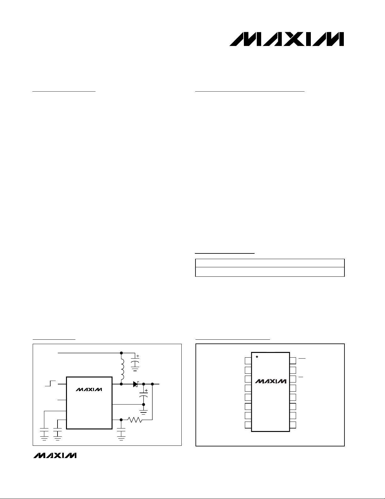
Pin Configuration
ONA
REF
SS/LIM
CLK
OUTPUT
3.3V, 5V,
OR ADJ
UP TO 4A
OUT
GND
LX
1µH
OFF
ON
INPUT
1V TO 5V
SYNC
OR
INTERNAL
MAX1709
Typical Operating Circuit
19-1724; Rev 0; 5/00
For free samples and the latest literature, visit www.maxim-ic.com or phone 1-800-998-8800.
For small orders, phone 1-800-835-8769.
Ordering Information
PART TEMP. RANGE PIN-PACKAGE
MAX1709ESE -40°C to +85°C 16 Narrow SO
TOP VIEW
1
ONA ONB
LX
2
LX
3
4
LX
GND
5
SS/LIM
6
REF
GND
7
8
16
15
CLK
14
3.3/5
MAX1709
NARROW SO
13
PGND
12
PGND
PGND
11
10
FB
9
OUT
Page 2
MAX1709
4A, Low-Noise, High-Frequency,
Step-Up DC-DC Converter
2 _______________________________________________________________________________________
ABSOLUTE MAXIMUM RATINGS
ELECTRICAL CHARACTERISTICS
(V
OUT
= V
CLK
= +3.6V, ONA = ONB = FB = GND, TA= 0°C to +85°C, unless otherwise noted. Typical values are at TA= +25°C.)
Stresses beyond those listed under “Absolute Maximum Ratings” may cause permanent damage to the device. These are stress ratings only, and functional
operation of the device at these or any other conditions beyond those indicated in the operational sections of the specifications is not implied. Exposure to
absolute maximum rating conditions for extended periods may affect device reliability.
ONA, ONB, OUT, SS/LIM, 3.3/5 to GND ...............-0.3V to +6.0V
LX to PGND ...........................................................-0.3V to +6.0V
FB, CLK, REF to GND.............................. -0.3V to (V
OUT
+ 0.3V)
PGND to GND .......................................................-0.3V to +0.3V
Continuous Power Dissipation (T
A
= +70°C)
16-Pin Narrow SO (derate 16.5mW/°C above +70°C) .....1.3W
Operating Temperature Range ...........................-40°C to +85°C
Junction Temperature......................................................+150°C
Storage Temperature ........................................-65°C to +150°C
Lead Temperature (soldering, 10s) .................................+300°C
Output Voltage VFB < 0.1V (Note 1)
Load Regulation Measured between 1A < ISW < 3A (Note 2) -
FB Regulation Voltage ISW = 1A
FB Input Current V
Output Voltage Adjust Range 2.5 5.5 V
Output Undervoltage Lockout (Note 3) 2.0 2.3 V
Frequency in Startup Mode V
Minimum Startup Voltage I
Minimum Operating Voltage (Note 5) 0.7 V
Soft-Start Pin Current V
OUT Supply Current VFB = 1.5V (Note 6) 200 440 µA
OUT Leakage Current In
Shutdown
LX Leakage Current VLX = V
N-Channel Switch
On-Resistance
N-Channel Current Limit
RMS Switch Current 10
Reference Voltage I
Reference Load Regulation -1µA ″ I
Reference Supply Rejection +2.5V ″ V
Input Low Level (Note 7)
PARAMETER CONDITIONS MIN TYP MAX UNITS
FB
= +1.5V
OUT
= 1.5V 40 400 kHz
OUT
< 1mA (Note 1), TA = +25°C (Note 4) 0.9 1.1 V
SS/LIM
= 1V 3.2 4 5.0 µA
ONB
V
= 3.6V 0.1 5 µA
ONB
= V
OUT
= +5.5V 0.1 40 µA
SS/LIM = open
SS/LIM = 150k to GND
REF
= 0
REF
″ 50µA410mV
OUT
″ +5.5V 0.2 5 mV
ONA,
CLK, 2.7V < V
, 3.3/5, 1.2V < V
ONB
OUT
< 5.5V
3.3/5 = GND, I
3.3/5 = OUT, I
SW
= 1A 3.26 3.34 3.42
SW
= 1A 4.92 5.05 5.17
-
1
200 nA
22 40 m
OUT
< 5.5V
7.5
3.5
9
5
12
6.5
x
OUT
x
OUT
V
%/A
V
Ω
A
RMS
V
V
Page 3
MAX1709
4A, Low-Noise, High-Frequency,
Step-Up DC-DC Converter
_______________________________________________________________________________________ 3
ELECTRICAL CHARACTERISTICS (continued)
(V
OUT
= V
CLK
= +3.6V, ONA = ONB = FB = GND, TA= 0°C to +85°C, unless otherwise noted. Typical values are at TA= +25°C.)
ELECTRICAL CHARACTERISTICS
(V
OUT
= V
CLK
= +3.6V, ONA = ONB = FB = GND, TA= -40°C to +85°C, unless otherwise noted.) (Note 9)
Input High Level
Logic Input Current ONA,
Internal Oscillator Frequency 520 600 680 kHz
Maximum Duty Cycle 82 90 94 %
External Clock Frequency
Range
CLK Pulse Width (Note 8) 100 ns
CLK Rise/Fall Time (Note 8) 50 ns
PARAMETER CONDITIONS MIN TYP MAX UNITS
ONA,
CLK, 2.7 V< V
, 3.3/5, 1.2V < V
ONB
< 5.5V
OUT
, CLK, 3.3/5 1 µA
ONB
OUT
< 5.5
x
x
350
V
V
OUT
OUT
Output Voltage
FB Regulation Voltage I
FB Input Current V
Load Regulation Measured between 1A < ISW < 5A (Note 2) -0.45 %/A
Soft-Start Pin Current SS/LIM = 1V 3.2 5.2 µA
OUT Leakage Current in
Shutdown
OUT Supply Current V
N-Channel Switch
On-Resistance
N-Channel Current Limit
Reference Voltage I
PARAMETER CONDITIONS MIN TYP MAX UNITS
VFB < 0.1V, V
(Note 1) 3.3/5 = OUT, I
= 1A 1.21 1.27 V
SW
= +1.5V 200 nA
FB
V
= 3.6V 5 µA
ONB
= 1.5V (Note 6) 400 µA
FB
SS/LIM = unconnected 7.5 15
SS/LIM = 150kΩ to GND 3.5 7
= 0 1.24 1.28 V
REF
= +2.4V 3.3/5 = GND, I
IN
= 1A 3.24 3.45
SW
= 1A 4.9 5.2
SW
40 mΩ
V
kHz
V
V
Page 4
Note 1: Output voltage is specified at 1A switch current ISW, which is equivalent to approximately 1A ✕(VIN/ V
OUT
) of load current.
Note 2: Load regulation is measured by forcing specified switch current and straight-line calculation of change in output voltage in
external feedback mode. Note that the equivalent load current is approximately I
SW
✕
(VIN/ V
OUT
).
Note 3: Until undervoltage lockout is reached, the device remains in startup mode. Do not apply full load until this voltage is
reached.
Note 4: Startup is tested with Figure 1’s circuit. Output current is measured when both the input and output voltages are applied.
Note 5: Minimum operating voltage. The MAX1709 is bootstrapped and will operate down to a 0.7V input once started.
Note 6: Supply current is measured from the OUT pin to the output voltage (+3.3V). This correlates directly with actual input supply
current but is reduced in value according to the step-up ratio and efficiency.
Note 7: ONA and ONB inputs have approximately 0.15V hysteresis.
Note 8: Guaranteed by design, not production tested.
Note 9: Specifications to -40°C are guaranteed by design, not production tested.
MAX1709
4A, Low-Noise, High-Frequency,
Step-Up DC-DC Converter
4 _______________________________________________________________________________________
ELECTRICAL CHARACTERISTICS (continued)
(V
OUT
= V
CLK
= +3.6V, ONA = ONB = FB = GND, TA= -40°C to +85°C, unless otherwise noted.) (Note 9)
Input Low Level (Note 7)
Input High Level
Logic Input Current ONA, ONB, CLK, 3.3/5 1 µA
Internal Oscillator Frequency 500 700 kHz
Maximum Duty Cycle 80 95 %
External Clock Frequency
Range
CLK/SEL Pulse Width (Note 8) 100 ns
CLK/SEL Rise/Fall Time (Note 8) 50 ns
PARAMETER CONDITIONS MIN TYP MAX UNITS
ONA, ONB, 3.3/5, 1.2V < V
CLK, 2.7V < V
ONA, ONB, 3.3/5, 1.2V < V
CLK, V
OUT
OUT
= 5.5V
< 5.5V
OUT
OUT
< 5.5V
< 5.5V
0.8 ×
V
OUT
0.8 ×
V
OUT
350 1000 kHz
0.2 ×
V
0.2 ×
V
OUT
OUT
V
V
Page 5
MAX1709
4A, Low-Noise, High-Frequency,
Step-Up DC-DC Converter
_______________________________________________________________________________________ 5
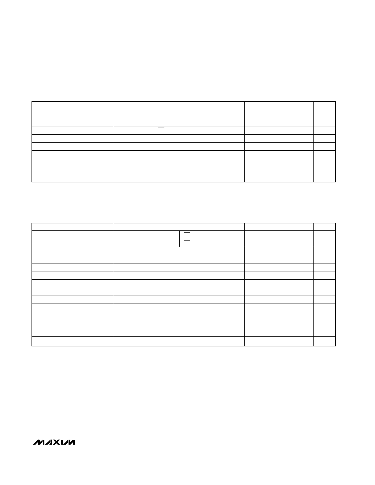
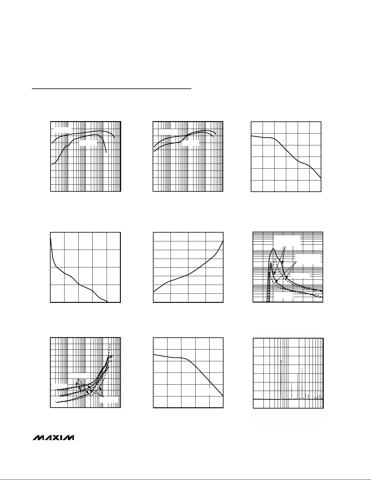
Typical Operating Characteristics
(TA = +25°C, unless otherwise noted.)
100
0
0.001 0.1 10.01 10
EFFICIENCY vs.
OUTPUT CURRENT (V
OUT
= 3.3V)
MAX1709 TOC01
OUTPUT CURRENT (A)
EFFICIENCY (%)
10
20
30
40
50
60
70
80
90
V
IN
= 2.5V
V
IN
= 1.2V
100
0
0.001 0.1 10.01 10
EFFICIENCY vs.
OUTPUT CURRENT (V
OUT
= 5V)
MAX1709 TOC02
OUTPUT CURRENT (A)
EFFICIENCY (%)
10
20
30
40
50
60
70
80
90
V
IN
= 3.3V
V
IN
= 2.5V
83.0
84.0
83.5
85.0
84.5
86.0
85.5
0.4 0.6 0.70.5 0.8 0.9 1.0
EFFICIENCY vs. SWITCHING FREQUENCY
(V
IN
= 3.3V, V
OUT
= 5V, I
OUT
= 2A)
MAX1709 TOC03
OPERATING FREQUENCY (MHz)
EFFICIENCY (%)
2
1
0
-1
-2
021 345
LOAD REGULATION
(V
IN
= 3.3V, V
OUT
= 5V)
MAX1709 TOC04
OUTPUT CURRENT (A)
V
OUT
REGULATION (%)
-0.8
-0.6
-0.4
-0.2
0
0.2
0.4
0.6
0.8
2.0 2.5 3.0 3.5 4.0
LINE REGULATION
(V
OUT
= 5V, I
OUT
= 1A)
MAX1709 TOC05
INPUT VOLTAGE (V)
V
OUT
REGULATION (%)
1000
0.1
01.00.5 2.0 3.5
NO-LOAD INPUT CURRENT
vs. INPUT VOLTAGE
1
10
100
MAX1709 TOC06
INPUT VOLTAGE (V)
INPUT CURRENT (mA)
1.5 2.5 3.0
V
OUT
= 3.3V
V
OUT
= 5V
INPUT VOLTAGE
INCREASING
INPUT VOLTAGE
DECREASING
2.8
0.6
0.001 0.1 10.01 10
STARTUP VOLTAGE
vs. LOAD CURRENT
MAX1709 TOC07
LOAD CURRENT (A)
STARTUP VOLTAGE (V)
1.0
0.8
1.2
1.4
1.6
1.8
2.0
2.2
2.4
2.6
TA = -40°C
T
A
= +25°C
TA = +85°C
V
OUT
= 3.3V
V
OUT
= 5V
-2.0
-1.0
-1.5
0
-0.5
0.5
1.0
-40 10 35-15 60 85
SWITCHING FREQUENCY
vs. TEMPERATURE
MAX1709 TOC08
TEMPERATURE (°C)
FREQUENCY CHANGE (%)
V
OUT
= 3.3V
-5
0.1 1 10
NOISE vs. FREQUENCY
5
0
MAX1709 TOC09
FREQUENCY (MHz)
NOISE (mV
RMS
)
15
10
20
25
30
-10
Page 6
MAX1709
4A, Low-Noise, High-Frequency,
Step-Up DC-DC Converter
6 _______________________________________________________________________________________
Typical Operating Characteristics (continued)
(Circuit of Figure 1, TA = +25°C, unless otherwise noted.)
SWITCH CURRENT LIMIT
vs. SS/LIM RESISTANCE
10
9
8
7
6
5
CURRENT LIMIT (A)
4
3
2
50 100 150 200 250 300
SS/LIM RESISTANCE (kΩ)
5V
0
5V
4A
2A
3A
1A
5V
6A
4A
2A
MAX1709 TOC10
HEAVY SWITCHING WAVEFORM
(WITH LC FILTER)
1µs/div
I
= 2A
OUT
L = 12.5nH (COILCRAFT A04T)
C = 1µF
LOAD-TRANSIENT
RESPONSE
20µs/div
SWITCH CURRENT LIMIT
vs. TEMPERATURE
11.5
11.0
10.5
10.0
9.5
CURRENT LIMIT (A)
9.0
8.5
8.0
-40 10-15 356085
MAX1709-13b
V
5V/div
V
100mV/div
I
2A/div
MAX1709-15
I
2A/div
V
100mV/div
I
2A/div
TEMPERATURE (°C)
LX
OUT
L
OUT
OUT
L
V
= 3.3V
OUT
5V
MAX1709-12
0
5V
4A
2A
LINE-TRANSIENT
3.5V
3V
5V
I
= 1A
OUT
SHUTDOWN WITH SOFT-START
(C
5V
0
4A
2A
0
4V
2V
CSS = 0.1µF
= 5Ω
R
OUT
= V
V
ONB
OUT
HEAVY SWITCHING WAVEFORM
I
= 2A
OUT
1µs/div
RESPONSE
100µs/div
= 0.1µF)
SS
1ms/div
MAX1709-14
MAX1709-16
V
0.5V/div
V
50mV/div
V
5V/div
I
2A/div
V
2V/div
MAX1709-13a
V
LX
5V/div
V
OUT
100mV/div
I
L
2A/div
IN
OUT
ONA
IN
OUT
Page 7
MAX1709
4A, Low-Noise, High-Frequency,
Step-Up DC-DC Converter
_______________________________________________________________________________________ 7
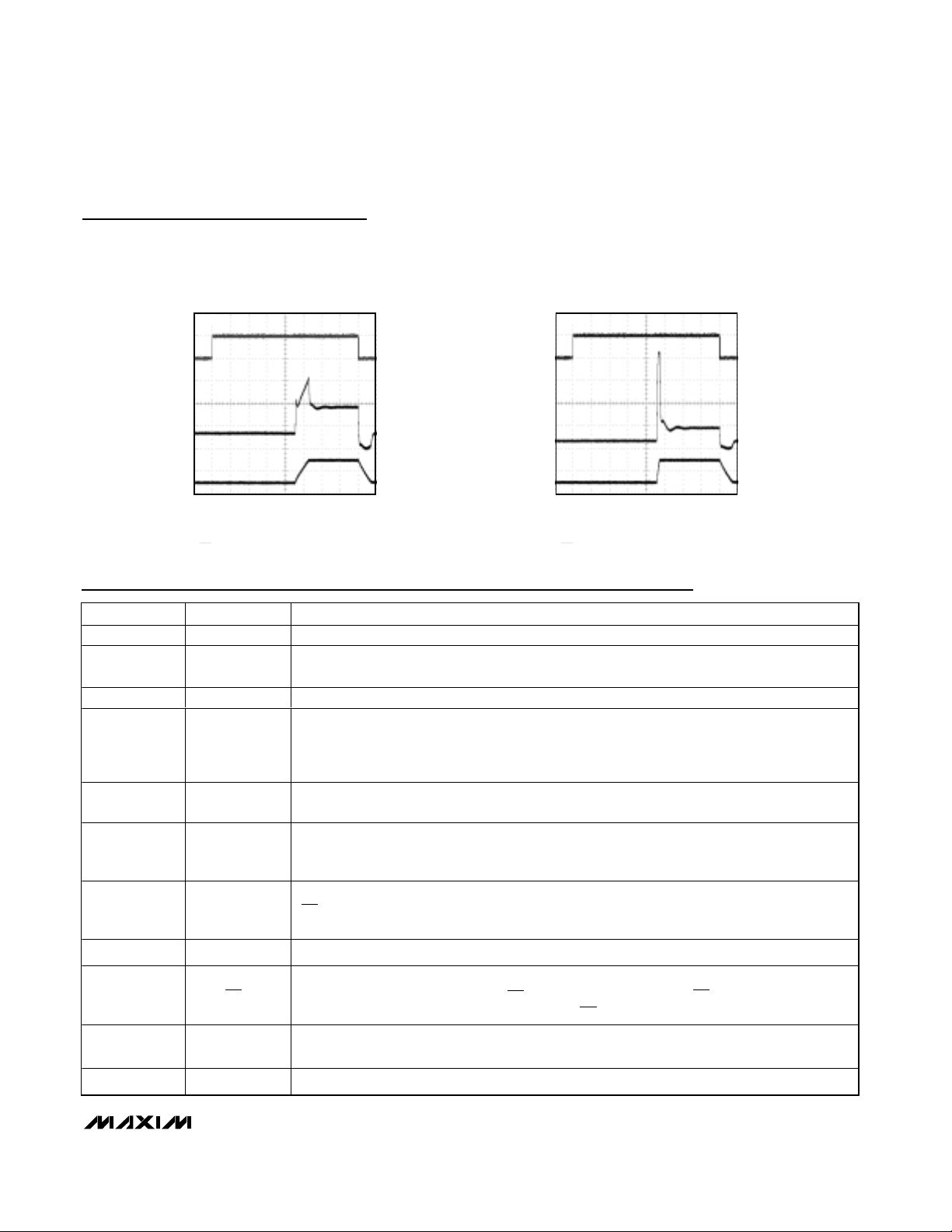
SHUTDOWN WITH SOFT-START
(C
SS
= 0.01µF)
MAX1709-17
5V
0
1ms/div
V
OUT
2V/div
V
ONA
5V/div
4A
0
4V
I
IN
2A/div
6A
2V
CSS = 0.01µF
R
OUT
= 5Ω
V
ONB
= V
OUT
2A
SHUTDOWN WITHOUT SOFT-START
MAX1709-18
5V
0
1ms/div
V
OUT
2V/div
V
ONA
5V/div
4A
0
4V
I
IN
2A/div
6A
2V
CSS = 0
R
OUT
= 5Ω
V
ONB
= V
OUT
2A
Typical Operating Characteristics (continued)
(Circuit of Figure 1, TA = +25°C, unless otherwise noted.)
Pin Description
PIN NAME FUNCTION
1 ONA On-Control Input. When ONA = high or ONB = low, the device turns on (Table 1).
2, 3, 4 LX
Drain of N-Channel Power Switch. Connect pins 2, 3, and 4 together. Connect external
Schottky diode from LX to OUT.
5, 8 GND Ground
6 SS/LIM
Soft-Start and/or Current-Limit Input. Connect a capacitor from SS/LIM to GND to control the
rate at which the device reaches current limit (soft-start). To reduce the current limit from the
preset values, connect a resistor from SS/LIM to GND (see Design Procedure). During
shutdown, this pin is internally pulled to GND to discharge the soft-start capacitor.
7 REF
1.26V Voltage Reference Output. Bypass with a 0.22µF capacitor to GND. Maximum REF load
is 50µA.
9 OUT
Output Voltage Sense Input. The device is powered from OUT. Bypass with a 0.1µF to PGND
with less than 5mm trace length. Connect a 2Ω series resistor from the output filter capacitor to
OUT (Figure 1).
10 FB
DC-DC Converter Feedback Input. Connect FB to GND for internally set output voltage (see
3.3/5 pin description). Connect a resistor-divider from the output to set the output voltage in
the +2.5V to +5.5V range. FB regulates to +1.25V (Figure 4).
11, 12, 13 PGND Power Ground, Source of N-Channel Power MOSFET Switch
14 3.3/5
Output Voltage Selection Pin. When FB is connected to GND, the regulator uses internal
feedback to set the output voltage. 3.3/5 = low sets output to 3.3V; 3.3/5 = high sets output to
5V. If an external divider is used at FB, connect 3.3/5 to ground.
15 CLK
Clock Input for the DC-DC Converter. Connect to OUT for internal oscillator. Optionally, drive
with an external clock for external synchronization.
16 ONB Shutdown Input. When ONB = high and ONA = low, the device turns off (Table 1).
Page 8

MAX1709
4A, Low-Noise, High-Frequency,
Step-Up DC-DC Converter
8 _______________________________________________________________________________________
_______________Detailed Description
The MAX1709 step-up converter offers high efficiency
and high integration for high-power applications. It
operates with an input voltage as low as 0.7V and is
suitable for single- to 3 cell battery inputs as well as
2.5V or 3.3V regulated supply inputs. The output voltage is preset to +3.3V or +5.0V or can be adjusted with
external resistors for voltages between +2.5V to +5.5V.
The MAX1709 internal N-channel MOSFET switch is
rated for 10A (RMS value) and can deliver loads to 4A,
depending on input and output voltages. For flexibility,
the current limit and soft-start rate are independently
programmable.
A 600kHz switching frequency allows for a small inductor to be used. The switching frequency is also synchronizable to an external clock ranging from 350kHz
to 1000kHz.
ONA,
ONB
The logic levels at ONA and ONB turn the MAX1709 on
or off. When ONA = 1 or ONB = 0, the part is on. When
ONA = 0 and ONB = 1, the part is off (Table 1). Logic
high on control can be implemented by tying ONB high
and using ONA for shutdown. Implement inverted sin-
gle-line on/off control by grounding ONA and toggling
ONB. Implement momentary pushbutton On/Off as
described in the Applications Information section. Both
inputs have approximately 0.15V of hysteresis.
Switching Frequency
The MAX1709 switches at the fixed-frequency internal
oscillator rate (600kHz) or can be synchronized to an
external clock. Connect CLK to OUT for internal clock
operation. Apply a clock signal to CLK to synchronize
to an external clock. The frequency can be changed on
the fly. The MAX1709 will synchronize to a new external
clock rate in two cycles and will take approximately
40µs to revert to its internal clock frequency once the
external clock pulses stop and CLK is driven high.
Table 2 summarizes oscillator operation.
Operation
The MAX1709 switches at a constant frequency
(600kHz) and modulates the MOSFET switch pulse
width to control the power transferred per cycle and
regulate the voltage across the load. In low-noise applications, the fundamental and the harmonics generated
by the fixed switching frequency are easily filtered out.
Figure 2 shows the simplified functional diagram for the
MAX1709. Figure 3 shows the simplified PWM con-
Figure 1. Standard Operating Circuit
KEEP TRACES
SHORT AND WIDE
ON-OFF
CONTROL
R1
C3
C4
0.22µF
ONA
LX
LX
LX
GND
SS/LIM
REF
GND
MAX1709
1µH
L1
D1
ONB
CLK
3.3/5
PGND
PGND
PGND
FB
OUT
C6, C7
2 x
150µF
C5
0.1µF
R2
2Ω
C1, C2
2 x 150µF
V
IN
1V TO 5V
V
OUT
5V
GND
Page 9

MAX1709
4A, Low-Noise, High-Frequency,
Step-Up DC-DC Converter
_______________________________________________________________________________________ 9
troller functional diagram. The MAX1709 enters synchronized current-mode PWM when a clock signal
(350kHz < f
CLK
< 1000kHz) is applied to CLK. For
wireless or noise-sensitive applications, this ensures
that switching harmonics are predictable and kept outside the IF frequency band(s). High-frequency operation permits low-magnitude output ripple voltage and
minimum inductor and filter capacitor size. Switching
losses will increase at the higher frequencies (see
Power Dissipation).
Setting the Output Voltage
The MAX1709 features Dual Mode™ operation. When
FB is connected to ground, the MAX1709 generates a
fixed output voltage of either +3.3V or +5V, depending
on the logic applied to the 3.3/5 input (Figure 1). The
output can be configured for other voltages, using two
external resistors as shown in Figure 4. To set the output voltage externally, choose an R3 value that is large
enough to minimize load at the output but small enough
to minimize errors due to leakage and the time constant
to FB. A value of R4
≤ 50kΩ is required.
where V
FB
= 1.24V.
Soft-Start/Current-Limit Adjustment
(SS/LIM)
The soft-start pin allows the soft-start time to be adjusted by connecting a capacitor from SS/LIM to ground.
Select capacitor C3 (connected to SS/LIM pin) as:
C3 (in µF) = 3.2 ✕t
SS
where tSSis the time (in seconds) it takes the switch
current limit to reach full value.
To improve efficiency or reduce inductor size at
reduced load currents, the current limit can be reduced
from its nominal value (see Electrical Characteristics).
A resistor (R1 in Figure 1) between SS/LIM and ground
reduces the current limit as follows:
_______________________________________________________________________________________
Figure 2. Simplified Functional Diagram
Table 2. Selecting Switching FrequencyTable 1. On/Off Logic Control
Dual Mode is a trademark of Maxim Integrated Products.
ONA ONB MAX1709
00On
0 1 Off
10On
11On
OUT
IC POWER
2.15V
ONA
ONB
REF
CLK
FB
3.3/5
GND
1.260V
UNDERVOLTAGE LOCKOUT
ON
RDY
REFERENCE
DUAL MODE
FB
OUT
MAX1709
STARTUP
EN Q
OSCILLATOR
EN
600kHz
OSCILLATOR
CLK MODE
0 Not allowed
1 PWM
External clock
(350kHz−1000kHz)
PWM
CONTROLLER
D
SEE
FIGURE 3.
EN
OSC
FB
V
OUT
V
FB
RR
34 1 =−
Synchronized PWM
LX
N
PGND
I
Rk
1 312 5 1 312 5
. .=×≤
1
ΩΩ
Rk
()
I
LIM
Page 10

MAX1709
4A, Low-Noise, High-Frequency,
Step-Up DC-DC Converter
10 ______________________________________________________________________________________
where I1is the desired current limit in amperes, and
I
LIM
is the current limit value from the Electrical
Characteristics.
__________________Design Procedure
Inductor Selection (L1)
The MAX1709’s high switching frequency allows the
use of a small-size inductor. Use a 1.0µH inductor for
600kHz operation. If the MAX1709 will be synchronized
at a different frequency, scale the inductor value with
the inverse of frequency (L1= 1µH ✕600kHz / f
SYNC
).
The PWM design tolerates inductor values within ±25%
of this calculated value, so choose the closest standard
inductor value. For example, use 1.5µH for 350kHz and
0.68µH for 1MHz).
Inductors with a ferrite core or equivalent are recommended; powder iron cores are not recommended for
use at high switching frequencies. Ensure the inductor’s saturation rating (the current at which the core
begins to saturate and inductance falls) exceeds the
internal current limit. Note that this current may be
reduced through SS/LIM if less than the MAX1709’s full
load current is needed (see Electrical Characteristics
for ratings). For highest efficiency, use a coil with low
DC resistance, preferably under 10mΩ. To minimize
radiated noise, use a toroid, pot core, or shielded
inductor. See Tables 3 and 4 for a list of recommended
components and component suppliers. To calculate
the maximum output current (in amperes), use the following equation:
where:
V
IN
= input voltage
VD= forward voltage drop of the Schottky diode at I
LIM
current
V
OUT
= output voltage
D' = (VIN) / (V
OUT
+ VD), assuming switch voltage drop
is negligible
f = switching frequency
L1 = inductor value
Table 4. Component Suppliers
Table 3. Component Selection Guide
Figure 3. Simplified PWM Controller Functional Diagram
Figure 4. Adjustable Output Voltage
PRODUCTION INDUCTORS CAPACITORS DIODES
Coilcraft DO3316P-102HC Panasonic EEFUE0J151R Motorola MBRD1035CTL
Surface mount
Coiltronics UP2B-1R0 Sanyo 6TPC100M
STM-Microelectronics
STPS8L30B
SUPPLIER PHONE FAX
Coilcraft 847-639-6400 847-639-1489
Coiltronics 561-241-7876 561-241-9339
Motorola 602-303-5454 602-994-6430
Panasonic 714-373-7939 714-373-7183
STMMicroelectronics
617-259-0300 617-259-9442
FB
REF
SLOPE
COMP
Q
R
S
LX
N
IDID
OUT MAX LIM
()
''=−
VVV
+−
OUT D IN
׃×
21
V
IN
LX
MAX1709
L
V
OUT
SS/LIM
(LIMITED TO 100mV)
12.5
OSCILLATOR
11mΩ
PGND
FB
KEEP SHORT
R4
R3
Page 11

MAX1709
4A, Low-Noise, High-Frequency,
Step-Up DC-DC Converter
______________________________________________________________________________________ 11
I
LIM
= minimum value of switch current limit from Elec-
trical Characteristics or set by R
SET/LIM
.
Diode Selection (D1)
The MAX1709’s high switching frequency demands a
high-speed rectifier. Schottky diodes, such as the
MBRD1035CTL or STPS8L30B (Table 3), are recommended. The diode’s current rating must exceed the
maximum load current, and its breakdown voltage must
exceed V
OUT
. The diode must be placed within 10mm
of the LX switching node and the output filter capacitor.
The diode also must be able to dissipate the power calculated by the following equation:
P
DIODE
= I
OUT
✕
V
D
where I
OUT
is the average load current and VDis the
diode forward voltage at the peak switch current.
Capacitor Selection
Input Bypass Capacitors (C1, C2)
Two 150µF, low-ESR tantalum input capacitors will
reduce peak currents and reflected noise due to inductor current ripple. Lower ESR allows for lower input ripple current, but combined ESR values up to 50mΩ are
acceptable. Smaller ceramic capacitors may also be
used for light loads or in applications that can tolerate
higher input current ripple.
Output Filter Capacitors (C6, C7)
The output filter capacitor ESR must be kept under
15mΩ for stable operation. Two parallel 150µF polymer
capacitors (Panasonic EEFUE0J151R) typically exhibit
5mΩ of ESR. This translates to approximately 35mV of
output ripple at 7A switch current. Bypass the
MAX1709 IC supply input (OUT) with a 0.1µF ceramic
capacitor to GND and a 2Ω series resistor (R2, as
shown in Figure 1).
MAX1709 IC Power Dissipation
The major components of MAX1709 dissipated power
are switch conductance loss (PSW), capacitive loss
(P
CAP
), and switch transition loss (P
TRAN
). Throughout
the formulas, numerical examples are provided in {},
corresponding to the following condition:
{VIN= 3.3V, V
OUT
= 5V, VD= 0.5V, I
OUT
= 4A}
An important parameter to compute the power dissipated in the MAX1709 is the approximate peak switch current (ISW):
PD(MAX1709) = PSW+ P
CAP
+ P
TRAN
{0.83W}
PSW= (1 - D') I
SW
2
✕
R
SW
{0.59W}
where:
RSW= switch resistance {33mΩ}
P
CAP
= (C
DIO
+ CDSW+ CGSW) (V
OUT
+ VD)2f {0.09W}
C
DIO
= catch-diode capacitance {1000pF}
CD
SW
= switch drain capacitance {2500pF}
CGSW= switch gate capacitance {1500pF}
f = switching frequency {600kHz}
P
TRAN
= (V
OUT
+ VD) I
SW
✕
t
SW
✕
f / 3 {0.15W}
where t
SW
= is switch turn-on or turn-off time {20ns}.
Applications Information
Using a Momentary On/Off Switch
A momentary pushbutton switch can be used to turn
the MAX1709 on and off. As shown in Figure 5, when
ONA is pulled low and ONB is pulled high, the part is
off. When the momentary switch is pressed, ONB is
pulled low and the regulator turns on. The switch
should be on long enough for the microcontroller to exit
reset. The controller issues a logic high to ONA, which
guarantees that the part will stay on regardless of the
subsequent switch state. To turn the regulator off,
press the switch long enough for the controller to read
the switch status and pull ONA low. When the switch is
released, ONB pulls high and the regulator turns off.
Layout Considerations
Due to high inductor current levels and fast switching
waveforms, proper PC board layout is essential. Protect
sensitive analog grounds by using a star ground config-
Figure 5. Momentary Pushbutton On-Off Switch
µ
270k
ON/OFF
0.1µF
MAX1709
ONB
ONA
270k
C
V
DD
I/O
I/O
I
I
SW
'
OUT
' {. }
=
D
=
D
VV
OUT D
V
IN
+
{.}
667
06
A
Page 12

MAX1709
4A, Low-Noise, High-Frequency,
Step-Up DC-DC Converter
Maxim cannot assume responsibility for use of any circuitry other than circuitry entirely embodied in a Maxim product. No circuit patent licenses are
implied. Maxim reserves the right to change the circuitry and specifications without notice at any time.
12 ____________________Maxim Integrated Products, 120 San Gabriel Drive, Sunnyvale, CA 94086 408-737-7600
© 2000 Maxim Integrated Products Printed USA is a registered trademark of Maxim Integrated Products.
Package Information
___________________Chip Information
TRANSISTOR COUNT: 1112
uration. Connect PGND, the input bypass capacitor
ground lead, and the output filter capacitor ground lead
to a single point (star ground configuration). In addition,
minimize trace lengths to reduce stray capacitance and
trace resistance, especially from the LX pins to the catch
diode (D1) and output capacitors (C6 and C7) to PGND
pins. If an external resistor-divider is used to set the output voltage (Figure 4), the trace from FB to the resistors
must be extremely short and must be shielded from
switching signals, such as CLK or LX. Refer to a layout
example in the MAX1709EVKIT data sheet.
SOICN.EPS
 Loading...