

Page 1
General Description
The MAX17083 is a fixed-frequency, current-mode,
step-down regulator optimized for low-voltage, lowpower applications. This regulator features dual internal
n-channel MOSFET power switches for high efficiency
and reduced component count. External Schottky
diodes are not required. An integrated boost switch
eliminates the need for an external boost diode. The
internal 25mΩ low-side power MOSFET easily supports
continuous load currents up to 5A. The MAX17083 produces an adjustable 0.75V to 2.7V output voltage from
the system’s 3.3V or 5V input supply.
This step-down regulator uses a peak current-mode
control scheme to eliminate the additional external
compensation required by voltage-mode architectures,
providing an easy-to-implement architecture without
sacrificing fast transient response. The MAX17083 provides peak current-limit protection and operates in
light-load pulse-skipping mode to maintain high efficiency under light-load conditions.
Independent enable input and open-drain power-good
output allow flexible system power sequencing. The voltage soft-start gradually ramps up the output voltage
within a predictable time period, effectively limiting the
inrush current. The MAX17083 features output undervoltage, output overvoltage, and thermal-fault protection.
The MAX17083 is available in a 24-pin 4mm x 4mm x
0.75mm TQFN package. The exposed backside pad
improves thermal characteristics.
Features
o Fixed-Frequency, Current-Mode Controller
o 2.4V to 5.5V Input Range
o Internal 5A Step-Down Regulator
o Internal BST Switch
o Fault Protection: Undervoltage, Overvoltage,
Thermal, Peak Current Limit
o Enable Input and Power-Good Output
o Voltage-Controlled Soft-Start
o High-Impedance Shutdown
o < 1µA (typ) Shutdown Current
MAX17083
Low-Voltage, Internal Switch,
Step-Down Regulator
________________________________________________________________
Maxim Integrated Products
1
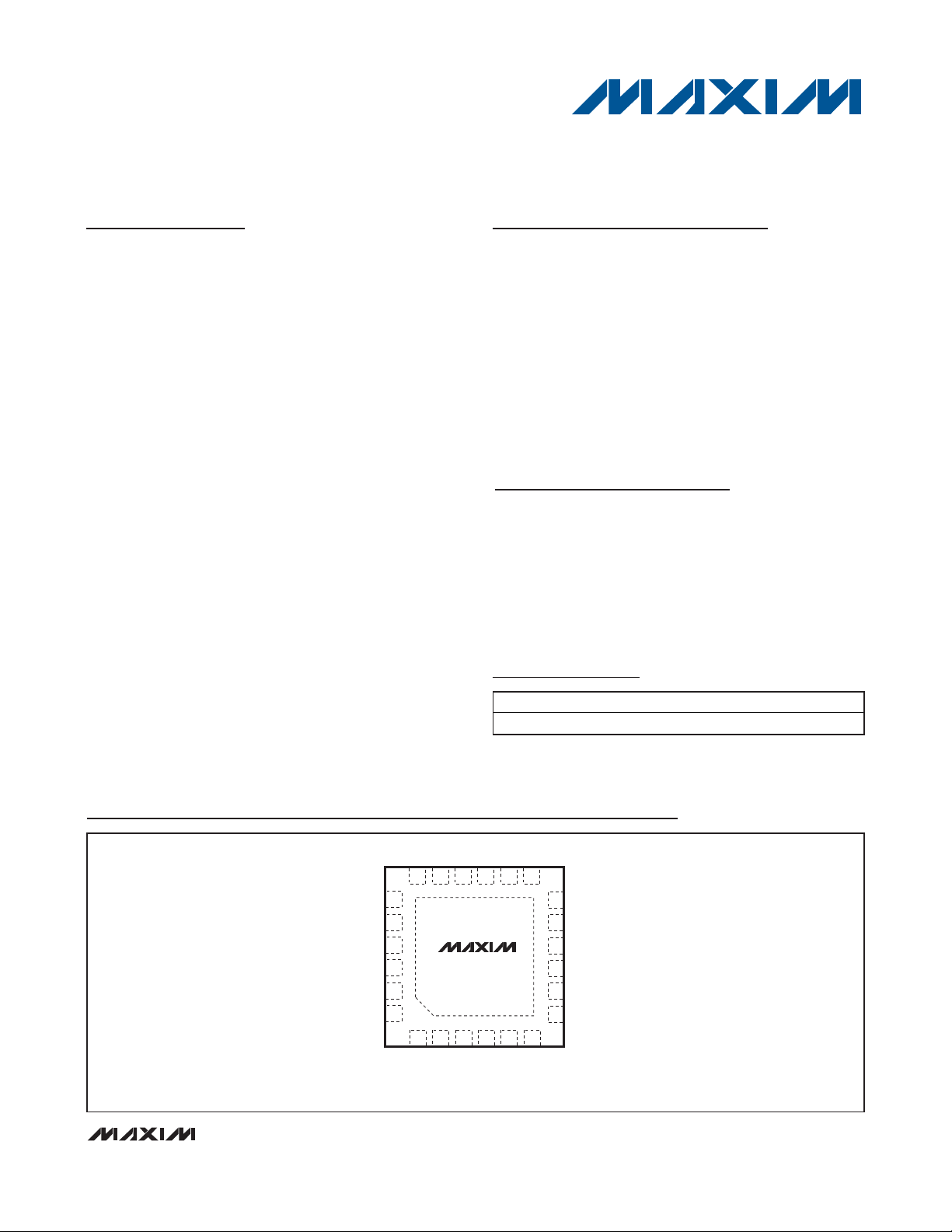
Pin Configuration
19-4458; Rev 0; 2/09
For pricing, delivery, and ordering information, please contact Maxim Direct at 1-888-629-4642,
or visit Maxim’s website at www.maxim-ic.com.
Ordering Information
PART TEMP RANGE PIN-PACKAGE
MAX17083ETG+ -40°C to +85°C 24 TQFN
+
Denotes a lead(Pb)-free/RoHS-compliant package.
Applications
Low-Power Architectures
Ultra-Mobile PCs
Netbook and Nettop PCs
Portable Gaming
Notebook and Subnotebook Computers
PDAs and Mobile Communicators
TOP VIEW
19
N.C.
20
PGND
21
PGND
PGND
22
PGND
23
N.C.
24
CC
BST
MAX17083
IN
TQFN
EN
V
IN
FREQ
LX
LX
18 17 16 15 14 13
+
12 3456
LX
LX
4mm x 4mm
SET
POK
12
FB
11
N.C.
10
GND
GND
9
GND
8
REF
7
Page 2
MAX17083
Low-Voltage, Internal Switch,
Step-Down Regulator
2 _______________________________________________________________________________________
ABSOLUTE MAXIMUM RATINGS
ELECTRICAL CHARACTERISTICS
(Circuit of Figure 1, V
IN
= V
FREQ
= VCC= VEN= 5V, I
REF
= no load, TA= 0°C to +85°C, unless otherwise noted. Typical values are at
T
A
= +25°C.)
Stresses beyond those listed under “Absolute Maximum Ratings” may cause permanent damage to the device. These are stress ratings only, and functional
operation of the device at these or any other conditions beyond those indicated in the operational sections of the specifications is not implied. Exposure to
absolute maximum rating conditions for extended periods may affect device reliability.
IN to PGND...............................................................-0.3V to +6V
V
CC
to GND..............................................................-0.3V to +6V
EN to GND................................................................-0.3V to +6V
REF, FB, SET, FREQ, POK to GND ............-0.3V to (V
CC
+ 0.3V)
LX to GND (Notes 1, 2)................................-0.6V to (V
IN
+ 0.3V)
BST to GND.........................................(V
CC
- 0.3V) to (VLX+ 6V)
GND to PGND (Note 2) .........................................-0.3V to +0.3V
REF Short-Circuit Current......................................................1mA
Continuous Power Dissipation, Multilayer PCB (T
A
= +70°C)
24-Pin, 4mm x 4mm TQFN
(derate 27.8mW/°C above +70°C) ........................2222mW
Operating Temperature Range ...........................-40°C to +85°C
Junction Temperature......................................................+150°C
Storage Temperature Range .............................-65°C to +150°C
Lead Temperature (soldering, 10s) .................................+300°C
PARAMETER SYMBOL CONDITIONS MIN TYP MAX UNITS
IN Input Voltage Range V
IN
2.4 5.5 V
VCC Input Voltage Range V
CC
4.5 5.5 V
IN Undervoltage Threshold No hy steresis 2.1 2.4 V
Vcc Undervoltage Threshold Rising edge, 160mV hysteresis 4.2 4.5 V
Shutdown Supply C urrent EN = GND, measured at VCC, TA = +25°C 0.1 1.0 μA
Supply Current Regulator enabled 65 95 μA
REFERENCE
Reference Output Voltage V
REF
No load 1.24 1.25 1.26 V
Reference Load Regulation -1μA < I
REF
< +50μA 3 10 mV
OSCILLATOR
Oscillator Frequency f
OSC
FREQ = GND 0.45 0.50 0.55 MHz
FREQ = VCC 1.50
FREQ = open 1.00
FREQ = REF 0.75
FREQ Settings
FREQ = GND 0.50
MHz
INTERNAL 5A STEP-DOWN CONVERTER
SET = GND 0.754 0.765 0.774
SET = REF 1.107 1.122 1.136
SET = open 1.51 1.53 1.55
FB Regulation Voltage
(No Load)
V
FB
No load
SET = 5V 1.812 1.836 1.86
V
SET = GND 0.72 0.774
SET = REF 1.07 1.136
SET = open 1.45 1.55
FB Regulation Voltage
(Full Load)
V
FB
I
OUT
= 4A
SET = 5V 1.76 1.86
V
Note 1: LX has clamp diodes to PGND and IN. If continuous current is applied through these diodes, thermal limits must be observed.
Note 2: Measurements valid using 20MHz bandwidth limit.
Page 3
MAX17083
Low-Voltage, Internal Switch,
Step-Down Regulator
_______________________________________________________________________________________ 3
PARAMETER SYMBOL CONDITIONS MIN TYP MAX UNITS
FB Load Regulation SET = GND -4 mV/A
FB Line Regulation
(Slope Compensation)
V
FB
SET = GND, 0 to 100% duty cycle,
V
CC
= 4.5V to 5.5V
10 15 20 mV
FB Input Current IFB SET = GND, TA= +25°C -100 -5 +100 nA
High-side n-channe l RDH 32 50
Internal MOSFET On-Resistance
(Note 3)
Low-side n-channel R
DL
17 30
m
Internal BST On-Resistance 2
LX Peak Current Limit 5 6 8 A
LX Idle Mode™ Trip Leve l 1.5 A
LX Zero-Crossing Trip Level 100 mA
Soft-Start Ramp Time T
SS
1939/
f
SW
ms
Soft-Start Fault Blanking Time T
SSLT
3232/
f
SW
ms
POK Upper Trip Threshold and
Overvoltage Fault Threshold
Rising edge, 50mV h ysteresi s 9 12 14 %
POK Lower Trip Threshold Fal ling edge, 50mV hysteresis -14 -12 -9 %
POK Pr opagation Dela y Time t
POK
FB forced 50mV beyond POK trip threshold 5 μs
Overvoltage Fault Latch
Delay Time
FB forced 50mV above POK upper trip
threshold
5 μs
Undervoltage Fault Latch
Delay Time
FB forced 50mV below POK lower trip
threshold, TUV
1534/
f
SW
ms
POK Output Low Voltage I
SINK
= 3mA 0.4 V
POK Leakage Current I
POK
SET = GND, FB = 1V (POK high impedance),
POK forced to 5.5V, T
A
= +25°C
1 μA
Thermal-Shutdown Threshold T
SHDN
Hysteresis = 15°C +160 °C
LOGIC INPUTS
EN Input High Threshold Rising, hysteresi s = 220mV (typ) 1.0 1.4 1.6 V
EN Input Bias Current TA = +25°C 0.1 1 μA
V
CC
VCC -
0.5
Open 3 3.2
REF 1.2 2.2
FREQ and SET Input Voltage
Levels
GND 0.5
V
FREQ and SET Input Bias
Currents
T
A
= +25°C -2 +0.1 +2 μA
ELECTRICAL CHARACTERISTICS (continued)
(Circuit of Figure 1, V
IN
= V
FREQ
= VCC= VEN= 5V, I
REF
= no load, TA= 0°C to +85°C, unless otherwise noted. Typical values are at
T
A
= +25°C.)
Idle Mode is a trademark of Maxim Integrated Products, Inc.
Page 4
Typical Operating Characteristics
(Circuit of Figure 1, V
IN
= 5V, V
OUT
= 1.1V, FREQ = open. TA= +25°C, unless otherwise noted.)
MAX17083
Low-Voltage, Internal Switch,
Step-Down Regulator
4 _______________________________________________________________________________________
ELECTRICAL CHARACTERISTICS
(Circuit of Figure 1, V
IN
= V
FREQ
= VCC= VEN= 5V, I
REF
= no load, TA= -40°C to +85°C, unless otherwise noted. Typical values are
at T
A
= +25°C.)
PARAMETER SYMBOL CONDITIONS MIN MAX UNITS
Shutdown Supply C urrent EN = GND, measured at VCC, TA = +25°C 10 μA
Supply Current
Regulator Enabled
Does not inc lude switching losses, measured
from V
CC
120 μA
REFERENCE
Reference Output Voltage V
REF
No load 1.145 1.265 V
INTERNAL 5A STEP-DOWN CONVERTER
LX Peak Current Limit 4.35 8 A
Note 3: Limits are 100% production tested at TA= +25°C. Maximum and minimum limits are guaranteed by design and
characterization.
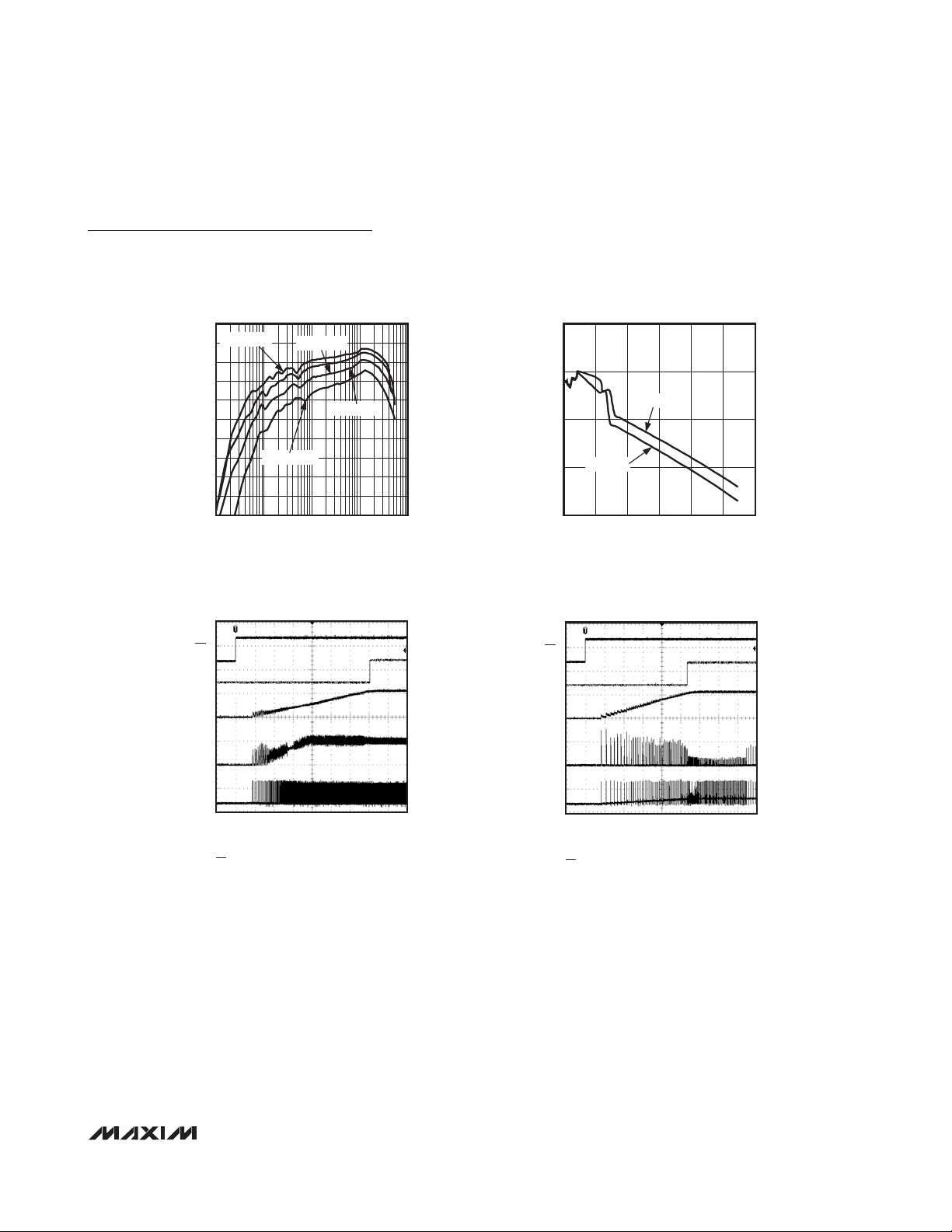
EFFICIENCY vs. LOAD CURRENT
100
V
= 1.8V
OUT
90
80
70
EFFICIENCY (%)
60
50
0.001 10
= 5V, 1MHz)
(V
IN
V
= 0.75V
OUT
0.01 0.1 1
LOAD CURRENT (A)
V
= 1.5V
OUT
V
= 1.1V
OUT
EFFICIENCY vs. LOAD CURRENT
= 3.3V, 1MHz)
(V
IN
V
= 1.5V
= 1.8V
V
0.01 0.1 1
OUT
= 0.75V
OUT
LOAD CURRENT (A)
MAX17083 toc02
V
= 1.1V
OUT
EFFICIENCY (%)
MAX17083 toc01
100
V
OUT
90
80
70
EFFICIENCY (%)
60
50
0.001 10
EFFICIENCY vs. LOAD CURRENT
= 5V, 750kHz)
(V
100
V
OUT
90
80
70
60
50
0.001 10
IN
V
= 1.5V
= 1.8V
0.01 0.1 1
OUT
V
= 0.75V
OUT
LOAD CURRENT (A)
V
= 1.1V
OUT
MAX17083 toc03
Page 5
MAX17083
Low-Voltage, Internal Switch,
Step-Down Regulator
_______________________________________________________________________________________ 5
Typical Operating Characteristics (continued)
(Circuit of Figure 1, V
IN
= 5V, V
OUT
= 1.1V, FREQ = open. TA= +25°C, unless otherwise noted.)
100
EFFICIENCY (%)
EFFICIENCY vs. LOAD CURRENT
V
OUT
90
80
70
60
50
0.001 10
REGULATOR STARTUP WAVEFORM
EN
= 3.3V, 750kHz)
(V
IN
= 1.8V
V
= 1.5V
OUT
V
OUT
V
= 0.75V
OUT
0.01 0.1 1
LOAD CURRENT (A)
(HEAVY LOAD)
= 1.1V
MAX17083 toc06
MAX17083 toc04
SMPS OUTPUT VOLTAGE
vs. LOAD CURRENT (1MHz)
0.78
0.77
VIN = 5V
0.76
OUTPUT VOLTAGE (V)
0.75
0.74
VIN = 3.3V
06
LOAD CURRENT (A)
42315
MAX17083 toc05
REGULATOR STARTUP WAVEFORM
(NO LOAD)
EN
MAX17083 toc07
POK
OUT
IL
LX
f
= 750kHz, VIN = 5V,
SW
= 1.1V
V
OUT
EN: 5V/div
OUT: 1V/div
400μs/div
R
= 0.22Ω
LOAD
POK: 2V/div
: 5A/div
I
L
LX: 5V/div
POK
OUT
IL
LX
= 1MHz, VIN = 5V,
f
SW
= 1.1V
V
OUT
EN: 5V/div
OUT: 1V/div
400μs/div
POK: 2V/div
: 5A/div
I
L
LX: 5V/div
Page 6

MAX17083
Low-Voltage, Internal Switch,
Step-Down Regulator
6 _______________________________________________________________________________________
Typical Operating Characteristics (continued)
(Circuit of Figure 1, V
IN
= 5V, V
OUT
= 1.1V, FREQ = open. TA= +25°C, unless otherwise noted.)
REGULATOR SHUTDOWN WAVEFORM
MAX17083 toc08
REGULATOR LOAD TRANSIENT
MAX17083 toc09
EN
OUT
POK
IL
LX
40
35
30
25
20
15
SAMPLE PERCENTAGE (%)
10
5
0
100μs/div
EN: 5V/div
OUT: 1V/div
POK: 2V/div
R
LOAD
: 2A/div
I
L
LX: 5V/div
OUTPUT VOLTAGE DISTRIBUTION
SET = GND (FB = 0.754V)
TA = +85°C
= +25°C
T
A
0.750
0.751
0.752
OUTPUT VOLTAGE (V)
0.753
0.754
SAMPLE SIZE = 100
0.755
0.756
= 0.55Ω
0.757
0.758
0.759
MAX17083 toc10
0.760
OUT
LX
IL
I
OUT
20μs/div
= V
EN = high, V
= 1.1V, 750kHz,
V
OUT
LOAD TRANSIENT IS FROM 1A TO 4A
= 5V,
IN
BIAS
LOAD REGULATION DISTRIBUTION
40
TA = +85°C
= +25°C
T
35
A
30
25
20
15
SAMPLE PERCENTAGE (%)
10
5
0
2.0
2.4
2.8
3.2
LOAD REGULATION (mV/A)
SAMPLE SIZE = 100
3.6
4.0
4.4
LX: 5V/div
: 2A/div
I
L
: 2A/div
I
OUT
4.8
5.2
MAX17083 toc11
5.6
6.0
PEAK CURRENT-LIMIT DISTRIBUTION
25
TA = +85°C
= +25°C
T
A
20
15
10
SAMPLE PERCENTAGE (%)
5
0
5.50
5.70
5.90
PEAK CURRENT LIMIT (A)
6.10
6.30
SAMPLE SIZE = 100
6.50
6.70
6.90
7.10
7.30
MAX17083 toc12
7.50
Page 7

MAX17083
Low-Voltage, Internal Switch,
Step-Down Regulator
_______________________________________________________________________________________ 7
Pin Description
PIN NAME FUNCTION
1, 2, 17, 18 LX
Inductor Connection for the Internal 5A Step-Down Con verter. Connect LX to the sw itched side of
the inductor.
3, 4 IN
Power Input Connection to the Drain of the Internal HS MOSFET. Bypass to PGND with a 10μF or
greater ceramic capacitor close to the IC to minimize parasitic inductance.
5 FREQ
Four-Level Switching Frequency (f
SW
) Selection Pin
FREQUENCY PIN SWITCHING FREQUENCY (MHz)
VCC 1.5
OPEN 1.0
REF 0.75
GND 0.5
6 POK
Open-Drain Power-Good Output. POK is pulled low if FB is more than 12% (typ) above or below the
nominal regulation thresho ld. POK is he ld low during soft-start and in shutdown. POK becomes
high impedance when FB is in regulation.
7 REF
1.25V Reference Voltage Output. B ypass REF to analog ground with a 0.1μF ceramic capacitor.
The reference sources up to 50μA for external loads. Loading REF degrades output voltage
accuracy according to the REF load regulation error.
8, 9, 10 GND Analog Ground
11, 19, 24 N.C. No Connection
12 FB
Feedback Input for the Internal 5A Step-Down Converter. FB regulation leve l can be preset b y the
SET pin.
13 SET
Four-Level FB Threshold Selection Pin
FB THRESHOLD SELECTION PIN
FB REGULATION VOLTAGE (V)
VCC 1.8
OPEN 1.5
REF 1.1
GND 0.75
14 V
CC
5V Bias Supply Input for the Internal Switching Regulator Drivers. Bypass wi th a 1μF or greater
ceramic capacitor. Provide s power for the BST driver supplies.
15 EN
Switching Regulator Enable Input. When EN is pulled low, LX is high impedance. When EN is
driven high, the controller enables the 5A internal switching regulator.
16 BST
Boost Flying Capacitor Connection for the Internal 5A Step-Down Converter. The MAX17083
includes an internal boost switch/diode connected between V
CC
and BST. Connect to an external
0.1μF ceramic capacitor as shown in Figure 1.
20–23 PGND Power Ground
EP GND Ground. Connect the exposed backside pad to analog ground.
Page 8

MAX17083
Low-Voltage, Internal Switch,
Step-Down Regulator
8 _______________________________________________________________________________________
Detailed Description
The MAX17083 standard application circuit (Figure 1)
provides a single 1.1V/5A chipset supply. The
MAX17083 features a step-down switching regulator
with dual internal n-channel MOSFET power switches.
These step-down regulators use a fixed-frequency, current-mode control scheme compensated by the output
capacitor, providing an easy-to-implement architecture
without sacrificing fast transient response. These regulators also provide peak current-limit protection, and
operate pulse-skipping mode at light loads to maintain
high efficiency.
Independent enable input and open-drain power-good
output allow flexible system power sequencing. The
voltage soft-start gradually ramps up the output voltage
within a predictable time period and reduces inrush
current. The MAX17083 features outputs undervoltage,
output overvoltage, and thermal-fault protection.
Reference (REF)
The 1.25V reference is accurate to ±1% over temperature and load, making REF useful as a precision system
reference. Bypass REF to GND with a 0.1µF or greater
ceramic capacitor. The reference sources up to 50µA
and sinks 5µA to support external loads. If highly accurate specifications are required for the main SMPS output voltages, the reference should not be loaded.
Loading the reference slightly reduces the output voltage accuracy because of the reference load-regulation
error as defined in the
Electrical Characteristics
table.
Figure 1. Standard Application Circuit
SET
V
CC
OPEN 1.5
REF 1.1
GND 0.75
FREQ
V
CC 1.5
OPEN 1.0
REF 0.75
GND 0.5
FB REGULATION
VOLTAGE (V)
1.8
SWITCHING
FREQUENCY (MHz)
OFFON
1μF
0.1μF
V
C1
C3
(OPEN)
CC
EN
SET
MAX17083
REF
FREQ
GND (EP)
BST
POK
IN
LX
FB
C
OUT
2x 10μF
C
BST
0.1μF
R4
100kΩ
L1
1μH
220μF, 6m Ω
V
CC
C
OUT
5V INPUT
OUTPUT
1.1V AT 5A
Page 9

MAX17083
Low-Voltage, Internal Switch,
Step-Down Regulator
_______________________________________________________________________________________ 9
Figure 2. MAX17083 Block Diagram
CC
BSTV
REF
FREQ
POK
SET
POR
REF
4 LVL DET
EN
1.4V RISING
OSC
CLK
UVLO
CONTROLLER
UVLO
V
CC
MAX17083
IN
LX
LOGIC
4 LVL DET
THERMAL
FAULT
+160°C
UV FAULT
TIMER
BLOCK
0V
COMP
ZX
ILIM_VALLEY
ILIM_PK
ISKIP
PWM
COMP
1.12 x FB_INT
EA THR
FB_INT
PGND
FB
UV
COMP
0.88 x FB_INT
Page 10

MAX17083
SMPS Detailed Description
Fixed-Frequency,
Current-Mode PWM Controller
The heart of the current-mode PWM controller is a multistage, open-loop comparator that compares the output
voltage-error signal with respect to the reference voltage, the current-sense signal, and the slope compensation ramp (Figure 2). The MAX17083 uses a directsumming configuration, approaching ideal cycle-tocycle control over the output voltage without a traditional
error amplifier and the phase shift associated with it.
Frequency Selection (FREQ)
The FREQ input selects the PWM mode switching frequency. FREQ is a four-level input to set the regulator
switching frequency. The regulator’s switching frequency is set according to Table 1, and latched at the
beginning of soft-start. High-frequency (FREQ = VCC)
operation optimizes the application for the smallest
component size, trading off efficiency due to higher
switching losses. This might be acceptable in ultraportable devices where the load currents are lower.
Low-frequency (FREQ = GND) operation offers the best
overall efficiency at the expense of component size and
board space.
FB Regulation Selection (SET)
The SET input selects one of the four preset feedback
regulation voltage levels. The SET pin is a four-level
input signal to set the FB regulation voltage. The regulator’s feedback regulation voltage is set according to
Table 2, and latched at the beginning of soft-start.
Adjustable Output-Voltage Operation Mode
The MAX17083 produces an adjustable 0.75V to 2.7V
output voltage from the system’s 3.3V or 5V input supply by using a resistive feedback divider. Set FB to
0.75V (SET = GND) in adjustable mode.
Light-Load Operation
An inherent automatic switchover to pulse-skipping
(PFM operation) takes place at light loads. This
switchover is affected by a comparator that truncates
the low-side switch on-time at the inductor current’s
zero crossing. The zero-crossing comparator senses
the inductor current during the off-time. Once the current through the low-side MOSFET drops below 100mA,
the zero-crossing comparator, turns off the low-side
MOSFET. This prevents the inductor from discharging
the output capacitors and forces the switching regulator to skip pulses under light-load conditions to avoid
overcharging the output.
Idle-Mode Current-Sense Threshold
When MAX17083 operates in pulse-skipping mode, the
on-time of the step-down controller terminates when
both the output voltage exceeds the feedback threshold, and the current-sense voltage exceeds the idlemode current-sense threshold. Under light-load
conditions, the on-time duration depends solely on the
idle-mode current-sense threshold. This forces the controller to source a minimum amount of power with each
cycle. To avoid overcharging the output, another ontime cannot be initiated until the output voltage drops
below the feedback threshold. Since the zero-crossing
comparator prevents the switching regulator from sinking current, the MAX17083 switching regulator must
skip pulses. Therefore, the controller regulates the
valley of the output ripple under light-load conditions.
The minimum idle-mode current requirement causes
the threshold between pulse-skipping PFM operation
and constant PWM operation to coincide with the
boundary between continuous and discontinuous
inductor-current operation (also known as the critical
conduction point). The load-current level at which
PFM/PWM crossover occurs (I
LOAD(SKIP)
) is equivalent
to half the idle-mode current threshold (see the
Electrical Characteristics
table for the idle-mode threshold of the regulator). The switching waveforms can
appear noisy and asynchronous at light-load pulseskipping operation, but this is a normal operating condition that results in high light-load efficiency.
Trade-offs in PFM noise and light-load efficiency are
made by varying the inductor value. Generally, low
inductor values produce a broader efficiency vs. load
Low-Voltage, Internal Switch,
Step-Down Regulator
10 ______________________________________________________________________________________
FREQ P IN
SELECT
SWITCHING
FREQ, f
SW
SOFT-START
TIME (ms)
1833/f
SW
STARTUP
BLANKING
TIME (ms)
3055/f
SW
VCC 1.5MHz 1.22 2.0
Open 1MHz 1.83 3.1
REF 750kHz 2.44 4.1
GND 500kH z 3.67 6.1
Table 1. MAX17083 FREQ Table
SET PIN SELECT FB REGULATION VOLTAGE (V)
VCC 1.8
Open 1.5
REF 1.1
GND 0.75
Table 2. MAX17083 SET Table
Page 11

MAX17083
Low-Voltage, Internal Switch,
Step-Down Regulator
______________________________________________________________________________________ 11
curve, while higher values result in higher full-load efficiency (assuming that the coil resistance remains fixed)
and less output voltage ripple. Penalties for using higher inductor values include larger physical size and
degraded load-transient response (especially at low
input-voltage levels).
SMPS POR, UVLO, and Soft-Start
Power-on reset (POR) occurs when VCCrises above
approximately 2.1V, resetting the undervoltage, overvoltage, and thermal-shutdown fault latches. The V
CC
input undervoltage lockout (UVLO) circuitry prevents
the switching regulators from operating if the 5V bias
supply (VCC) is below its 4V UVLO threshold.
Soft-Startup
The internal step-down controller starts switching and the
output voltages ramp up using soft-start. If the bias supply
voltage drops below the UVLO threshold, the controller
stops switching and disables the drivers (LX becomes
high impedance) until the bias supply voltage recovers.
Once the 5V bias supply and IN rise above their respective input UVLO thresholds, and EN is pulled high, the
internal step-down controller becomes enabled and
begins switching. The internal voltage soft-starts gradually increment the feedback voltage by approximately
25mV every 61 switching cycles. Therefore, OUT reaches its nominal regulation voltage 1833/fSWafter the regulator is enabled (see the Soft-Start Waveforms in the
Typical Operating Characteristics
section).
SMPS Power-Good Output (POK)
POK is the open-drain output of the window comparator
that continuously monitors the output for undervoltage
and overvoltage conditions. POK is actively held low in
shutdown (EN = GND) and during soft-start. Once the
soft-start sequence terminates, POK becomes high
impedance as long as the output remains within ±10%
of the nominal regulation voltage set by FB. POK goes
low once the output drops 12% (typ) below or rises 12%
(typ) above its nominal regulation point, or the output is
shut down. For a logic-level POK output voltage, connect an external pullup resistor between POK and VCC.
A 100kΩ pullup resistor works well in most applications.
SMPS Fault Protection
Output Overvoltage Protection (OVP)
If the output voltage rises above 112% (typ) of its nominal regulation voltage, the controller sets the fault latch,
pulls POK low, shuts down the regulator, and immediately pulls the output to ground through its low-side
MOSFET. Turning on the low-side MOSFET with 100%
duty cycle rapidly discharges the output capacitors and
clamps the output to ground. However, this commonly
undamped response causes negative output voltages
due to the energy stored in the output LC at the instant
of 0V fault. If the load cannot tolerate a negative voltage,
place a power Schottky diode across the output to act
as a reverse-polarity clamp. If the condition that caused
the overvoltage persists (such as a shorted high-side
MOSFET), the input source also fails (short-circuit fault).
Cycle VCCbelow 1V or toggle the enable input to clear
the fault latch and restart the regulator.
Output Undervoltage Protection (UVP)
Each MAX17083 includes an output undervoltage
(UVP) protection circuit that begins to monitor the output once the startup blanking period has ended. If the
output voltage drops below 88% (typ) of its nominal
regulation voltage, the regulator pulls the POK output
low and begins the UVP fault timer. Once the timer
expires after 1600/fSW, the regulator shuts down, forcing the high-side off and disabling the low-side MOSFET once the zero-crossing threshold has been
reached. Cycle VCCbelow 1V, or toggle the enable
input to clear the fault latch and restart the regulator.
Thermal-Fault Protection
The MAX17083 features a thermal-fault protection
circuit. When the junction temperature rises above
+160°C (typ), a thermal sensor activates the fault latch,
pulls down the POK output, and shuts down the regulator. Toggle EN to clear the fault latch, and restart the
controllers after the junction temperature cools by
15°C (typ).
SMPS Design Procedure
(Step-Down Regulator)
Firmly establish the input voltage range and maximum
load current before choosing a switching frequency
and inductor operating point (ripple-current ratio). The
primary design trade-off lies in choosing a good switching frequency and inductor operating point, and the following four factors dictate the rest of the design:
• Input Voltage Range. The maximum value (V
IN(MAX)
),
and minimum value (V
IN(MIN)
) must accommodate
the worst-case conditions accounting for the input
voltage soars and drops. If there is a choice at all,
lower input voltages result in better efficiency.
• Maximum Load Current. There are two values to
consider. The peak load current (I
LOAD(MAX)
) determines the instantaneous component stresses and filtering requirements and thus drives output-capacitor
selection, inductor-saturation rating, and the design of
the current-limit circuit. The continuous load current
Page 12

(I
LOAD
) determines the thermal stresses and thus drives the selection of input capacitors, MOSFETs, and
other critical heat-contributing components.
• Switching Frequency. This choice determines the
basic trade-off between size and efficiency. The
optimal frequency is largely a function of maximum
input voltage due to MOSFET switching losses that
are proportional to frequency and the square of VIN.
The optimum frequency is also a moving target, due
to rapid improvements in MOSFET technology that
are making higher frequencies more practical.
• Inductor Operating Point. This choice provides
trade-offs between size and efficiency, and
between transient response and output ripple. Low
inductor values provide better transient response
and smaller physical size, but also result in lower
efficiency and higher output ripple due to increased
ripple currents. The minimum practical inductor
value is one that causes the circuit to operate at the
edge of critical conduction (where the inductor current just touches zero with every cycle at maximum
load). Inductor values lower than this grant no further size-reduction benefit. The optimum operating
point is usually found between 20% and 50% of ripple current. When pulse skipping (at light loads),
the inductor value also determines the load-current
value at which PFM/PWM switchover occurs.
Step-Down Inductor Selection
The switching frequency and inductor operating point
determine the inductor value as follows:
Assuming 5A maximum load current, and an LIR of 0.3
yields:
Find a low-loss inductor having the lowest possible DC
resistance that fits in the allotted dimensions. Most
inductor manufacturers provide inductors in standard
values, such as 1.0µH, 1.5µH, 2.2µH, 3.3µH, etc. Also
look for nonstandard values, which can provide a better
compromise in LIR across the input voltage range. If
using a swinging inductor (where the no-load inductance decreases linearly with increasing current), evaluate the LIR with properly scaled inductance values. For
the selected inductance value, the actual peak-to-peak
inductor ripple current (ΔI
INDUCTOR
) is defined by:
Ferrite cores are often the best choice, although soft saturating molded core inductors are inexpensive and can
work well at 500kHz. The core must be large enough not
to saturate at the peak inductor current (I
PEAK
):
SMPS Output-Capacitor Selection
The output filter capacitor selection requires careful
evaluation of several different design requirements—
stability, transient response, and output ripple voltage—that place limits on the output capacitance and
ESR. Based on these requirements, the typical application requires a low-ESR polymer capacitor (lower cost
but higher output-ripple voltage) or bulk ceramic
capacitors (higher cost but low output-ripple voltage).
SMPS Loop Compensation
Voltage positioning dynamically lowers the output voltage in response to the load current, reducing the loop
gain. This reduces the output capacitance requirement
(stability and transient) and output power dissipation
requirements as well. The load-line is generated by
sensing the inductor current through the high-side
MOSFET on-resistance, and is internally preset to
-5mV/A (typ). The load-line ensures that the output voltage remains within the regulation window over the fullload conditions.
The load line of the internal SMPS regulators also provides the AC ripple voltage required for stability. To
maintain stability, the output capacitive ripple must be
kept smaller than the internal AC ripple voltage, and
crossover must occur before the Nyquist pole occurs
(1 + duty)/(2fSW). Based on these loop requirements, a
minimum output capacitance can be determined from
the following:
where R
DROOP
is 5mV/A as defined in the
Electrical
Characteristics
table and fSWis the switching frequen-
cy selected by the FREQ setting (see Table 1).
C
fR
V
V
V
V
OUT
SW DROOP
REF
OUT
OUT
>
⎛
⎝
⎜
⎞
⎠
⎟
⎛
⎝
⎜
⎞
⎠
⎟
+
1
2
1
IIN
⎛
⎝
⎜
⎞
⎠
⎟
II
I
PEAK LOAD MA X
INDUCTOR
=+
⎛
⎝
⎜
⎞
⎠
⎟
()
Δ
2
ΔI
VVV
Vf L
INDUCTOR
OUT IN OUT
IN OSC
=
()
-
L
VVV
Vf
OUT IN OUT
IN OSC
=
×
()
××
-
15.
L
VVV
Vf I LIR
OUT IN OUT
IN OSC LOAD MAX
=
×
()
×× ×
-
()
MAX17083
Low-Voltage, Internal Switch,
Step-Down Regulator
12 ______________________________________________________________________________________
Page 13

MAX17083
Low-Voltage, Internal Switch,
Step-Down Regulator
______________________________________________________________________________________ 13
Additionally, an additional feedback pole—capacitor
from FB to analog ground (CFB)—might be necessary to
cancel the unwanted ESR zero of the output capacitor.
In general, if the ESR zero occurs before the Nyquist
pole, then canceling the ESR zero is recommended.
If:
Then:
where RFBis the parallel impedance of the FB resistive
divider.
SMPS Output Ripple Voltage
With polymer capacitors, the effective series resistance
(ESR) dominates and determines the output ripple voltage. The step-down regulator’s output ripple voltage
(V
RIPPLE
) equals the total inductor ripple current
(ΔI
INDUCTOR
) multiplied by the output capacitor’s ESR.
Therefore, the maximum ESR to meet the output ripple
voltage requirement is:
where fSWis the switching frequency. The actual capacitance value required relates to the physical case size
needed to achieve the ESR requirement, as well as to
the capacitor chemistry. Thus, polymer capacitor selection is usually limited by ESR and voltage rating rather
than by capacitance value. Alternatively, combining
ceramics (for the low ESR) and polymers (for the bulk
capacitance) helps balance the output capacitance vs.
output ripple voltage requirements.
Internal SMPS Transient Response
The load-transient response depends on the overall output impedance over frequency, and the overall amplitude
and slew rate of the load step. In applications with large,
fast load transients (load step > 80% of full load and slew
rate > 10A/µs), the output capacitor’s high-frequency
response—ESL and ESR—needs to be considered. To
prevent the output voltage from spiking too low under a
load-transient event, the ESR is limited by the following
equation (ignoring the sag due to finite capacitance):
where V
STEP
is the allowed voltage drop, ΔI
LOAD(MAX)
is
the maximum load step, and R
PCB
is the parasitic board
resistance between the load and output capacitor.
The capacitance value dominates the midfrequency
output impedance and continues to dominate the loadtransient response as long as the load transient’s slew
rate is fewer than two switching cycles. Under these
conditions, the sag and soar voltages depend on the
output capacitance, inductance value, and delays in
the transient response. Low inductor values allow the
inductor current to slew faster, replenishing charge
removed from or added to the output filter capacitors
by a sudden load step, especially with low differential
voltages across the inductor. The sag voltage (V
SAG
)
that occurs after applying the load current can be estimated by the following:
where D
MAX
is the maximum duty factor (see the
Electrical Characteristics
table), T is the switching period
(1/f
OSC
), and ΔT equals V
OUT/VIN
x T when in PWM
mode, or L x I
IDLE
/(VIN- V
OUT
) when in pulse-skipping
mode. The amount of overshoot voltage (V
SOAR
) that
occurs after load removal (due to stored inductor energy)
can be calculated as:
When using low-capacity ceramic filter capacitors,
capacitor size is usually determined by the capacity
needed to prevent V
SOAR
from causing problems during
load transients. Generally, once enough capacitance is
added to meet the overshoot requirement, undershoot at
the rising load edge is no longer a problem.
Input-Capacitor Selection
The input capacitor must meet the ripple current
requirement (I
RMS
) imposed by the switching currents.
The I
RMS
requirements of the regulator can be deter-
mined by the following equation:
The worst-case RMS current requirement occurs when
operating with VIN= 2V
OUT
. At this point, the above
equation simplifies to I
RMS
= 0.5 x I
LOAD.
I
I
V
VVV
RMS
LOAD
IN
OUT IN OUT
=
⎛
⎝
⎜
⎞
⎠
⎟
()
-
V
IL
CV
SOA R
LOAD MAX
OUT OUT
≈
()
Δ
()
2
2
V
LI
CVD V
I
SAG
LOAD MAX
OUT IN MAX OUT
=
()
×
()
+
Δ
Δ
()
2
2 -
LLOAD MAX
OUT
TT
C
()
- Δ
()
R
V
I
R
ESR
STEP
LOAD MAX
PCB
≤
⎛
⎝
⎜
⎞
⎠
⎟
Δ
()
-
R
Vf L
VV V
V
ESR
IN SW
IN OUT OUT
RI PPLE
≤
()
⎡
⎣
⎢
⎢
⎤
⎦
⎥
⎥
-
C
C ESR
R
FB
OUT
FB
>
⎛
⎝
⎜
⎞
⎠
⎟
ESR
D
fC
SW OUT
>
+
⎛
⎝
⎜
⎞
⎠
⎟
1
4π
Page 14

For the MAX17083 system (IN) supply, ceramic capacitors are preferred due to their resilience to inrush surge
currents typical of systems, and due to their low parasitic inductance, which helps reduce the high-frequency ringing on the IN supply when the internal MOSFETs
are turned off. Choose an input capacitor that exhibits
less than +10°C temperature rise at the RMS input current for optimal circuit longevity.
BST Capacitors
The boost capacitor (C
BST
) must be selected large
enough to handle the gate charging requirements of
the high-side MOSFETs. For these low-power applications, 0.1µF ceramic capacitors work well.
Applications Information
Duty-Cycle Limits
Minimum Input Voltage
The minimum input operating voltage (dropout voltage)
is restricted by the maximum duty-cycle specification
(see the
Electrical Characteristics
table). For the best
dropout performance, use the slowest switching frequency setting (FREQ = GND). However, keep in mind
that the transient performance gets worse as the stepdown regulators approach the dropout voltage, so bulk
output capacitance must be added (see the voltage
sag and soar equations in the
SMPS Design Procedure
section). The absolute point of dropout occurs when the
inductor current ramps down during the off-time
(ΔI
DOWN
) as much as it ramps up during the on-time
(ΔIUP). This results in a minimum operating voltage
defined by the following equation:
where V
CHG
and V
DIS
are the parasitic voltage drops in
the charge and discharge paths, respectively. A reasonable minimum value for h is 1.5, while the absolute
minimum input voltage is calculated with h = 1.
Maximum Input Voltage
The MAX17083 controller includes a minimum on-time
specification, which determines the maximum input
operating voltage that maintains the selected switching
frequency (see the
Electrical Characteristics
table).
Operation above this maximum input voltage results in
pulse skipping to avoid overcharging the output. At the
beginning of each cycle, if the output voltage is still
above the feedback threshold voltage, the controller
does not trigger an on-time pulse, effectively skipping a
cycle. This allows the controller to maintain regulation
above the maximum input voltage, but forces the controller to effectively operate with a lower switching frequency. This results in an input threshold voltage at
which the controller begins to skip pulses (V
IN(SKIP)
):
where f
OSC
is the switching frequency selected by FREQ.
PCB Layout Guidelines
Careful PCB layout is critical to achieving low switching
losses and clean, stable operation. The switching power
stage requires particular attention. If possible, mount all
the power components on the top side of the board,
with their ground terminals flush against one another.
Follow the MAX17083 Evaluation Kit layout and use the
following guidelines for good PCB layout:
• Keep the high-current paths short, especially at the
ground terminals. This practice is essential for stable, jitter-free operation.
• Keep the power traces and load connections short.
This practice is essential for high efficiency. Using
thick copper PCBs (2oz vs. 1oz) can enhance fullload efficiency by 1% or more. Correctly routing
PCB traces is a difficult task that must be
approached in terms of fractions of centimeters,
where a single milliohm of excess trace resistance
causes a measurable efficiency penalty.
• When trade-offs in trace lengths must be made, it is
preferable to allow the inductor charging path to be
made longer than the discharge path. For example,
it is better to allow some extra distance between the
input capacitors and the high-side MOSFET than to
allow distance between the inductor and the lowside MOSFET or between the inductor and the output filter capacitor.
• Route high-speed switching nodes (BST and LX)
away from sensitive analog areas (REF and FB).
VV
ft
IN SKIP OUT
OSC ON MIN
()
()
=
⎛
⎝
⎜
⎞
⎠
⎟
1
VVVhDVV
IN MIN OUT CHG
MAX
OUT DIS()
=++
⎛
⎝
⎜
⎞
⎠
⎟
+
(
1
1-
))
MAX17083
Low-Voltage, Internal Switch,
Step-Down Regulator
14 ______________________________________________________________________________________
Page 15

MAX17083
Low-Voltage, Internal Switch,
Step-Down Regulator
Maxim cannot assume responsibility for use of any circuitry other than circuitry entirely embodied in a Maxim product. No circuit patent licenses are
implied. Maxim reserves the right to change the circuitry and specifications without notice at any time.
Maxim Integrated Products, 120 San Gabriel Drive, Sunnyvale, CA 94086 408-737-7600 ____________________
15
© 2009 Maxim Integrated Products Maxim is a registered trademark of Maxim Integrated Products, Inc.
Package Information
For the latest package outline information and land patterns, go
to www.maxim-ic.com/packages
.
Chip Information
PROCESS: BiCMOS
PACKAGE TYPE PACKAGE CODE DOCUMENT NO.
24 TQFN-EP T2444-4
21-0139
 Loading...