

Page 1
General Description
The MAX17067 boost converter incorporates highperformance (at 1.2MHz), current-mode, fixed-frequency,
pulse-width modulation (PWM) circuitry with a built-in
0.15Ω n-channel MOSFET to provide a highly efficient
regulator with fast response.
High switching frequency (640kHz or 1.2MHz selectable)
allows for easy filtering and faster loop performance. An
external compensation pin provides the user flexibility in
determining loop dynamics, allowing the use of small,
low equivalent-series-resistance (ESR) ceramic output
capacitors. The device can produce an output voltage
as high as 18V.
Soft-start is programmed with an external capacitor, which
sets the input-current ramp rate. The MAX17067 is available in a space-saving 8-pin μMAX
®
package. The ultrasmall package and high switching frequency allow the
total solution to be less than 1.1mm high.
Application
LCD Displays
Features
o 90% Efficiency
o Adjustable Output from V
IN
to 18V
o 2.4A, 0.15Ω, 22V Power MOSFET
o +2.6V to +4.0V Input Range
o Pin-Selectable 640kHz or 1.2MHz Switching
Frequency
o Programmable Soft-Start
o Small 8-Pin µMAX Package
o Integrated Input Voltage Clamp Circuit
MAX17067
Low-Noise Step-Up DC-DC Converter
________________________________________________________________
Maxim Integrated Products
1
Typical Operating Circuit
19-3106; Rev 0; 1/08
Pin Configuration
Ordering Information
For pricing, delivery, and ordering information, please contact Maxim Direct at 1-888-629-4642,
or visit Maxim’s website at www.maxim-ic.com.
EVALUATION KIT
AVAILABLE
μMAX is a registered trademark of Maxim Integrated Products, Inc.
+
Denotes a lead-free package.
PART TEMP RANGE
MAX17067EUA+ -40°C to +85°C 8 μMAX
PINPACKAGE
PKG
CODE
U8+1
V
IN
2.6V TO 4V
IN
ON/OFF
SHDN
MAX17067
FREQ
SS
LX
GND
FB
COMP
V
OUT
TOP VIEW
1
COMP
2
3
SHDN
4
8
SS
FREQFB
7
MAX17067
μMAX
6
IN
5
LXGND
Page 2
MAX17067
Low-Noise Step-Up DC-DC Converter
2 _______________________________________________________________________________________
ABSOLUTE MAXIMUM RATINGS
ELECTRICAL CHARACTERISTICS
(VIN= SHDN = 3V, FREQ = 3V, TA= 0°C to +85°C, unless otherwise noted. Typical values are at TA= +25°C.) (Note 2)
Stresses beyond those listed under “Absolute Maximum Ratings” may cause permanent damage to the device. These are stress ratings only, and functional
operation of the device at these or any other conditions beyond those indicated in the operational sections of the specifications is not implied. Exposure to
absolute maximum rating conditions for extended periods may affect device reliability.
LX to GND ..............................................................-0.3V to +22V
SHDN, FREQ to GND ............................................-0.3V to +7.5V
IN to GND (Note 1) ...................................................-0.3V to +6V
SS, COMP, FB to GND ................................-0.3V to (V
IN
+ 0.3V)
RMS LX Pin Current ..............................................................1.2A
Continuous Power Dissipation (T
A
= +70°C)
8-Pin μMAX (derate 4.1mW/°C above +70°C) ............330mW
Operating Temperature Range ...........................-40°C to +85°C
Junction Temperature......................................................+150°C
Storage Temperature Range .............................-65°C to +150°C
Lead Temperature (soldering, 10s) .................................+300°C
Input Supply Range VIN V
Output Voltage 18 V
Input Supply Clamp Voltage
VIN Undervoltage Lockout UVLO
Quiescent Current I
Shutdown Supply Current I
ERROR AMPLIFIER
Feedback Voltage VFB Level to produce V
FB Input Bias Current IFB VFB = 1.24V 50 125 200 nA
Feedback-Voltage Line
Regulation
Transconductance g
Voltage Gain AV 3800 V/V
OSCILLATOR
Frequency f
Max imum Dut y C ycle DC FREQ = GND, FREQ = IN 89 92 95 %
n-CHANNEL SWITCH
Current Lim it I
On-Resistance RON 150 275 m
Leakage Current I
Current-Sense Tran sres is tance RCS 0.2 0.3 0.4 V/A
SOFT-START
Reset Switch Res is tance 100
Charge Current VSS = 1.2V 2.5 4.5 6.5 μA
PARAMETER SYMBOL CONDITIONS MIN TYP MAX UNITS
< 18V 2.6 4.0 V
OUT
Use external limiting resistor; R
= 10V (Note 3)
V
IN
V
rising, typical hysteresis is 50mV, LX
IN
remains off below this level
VFB = 1.3V, not switching 0.3 0.6
IN
VFB = 1.0V, switching 1.5 2.5
SHDN = GND, TA = +25°C 30 60
IN
SHDN = GND, TA = +85°C 30
= 1.24V 1.23 1.24 1.25 V
COMP
Level to produce V
2.6V < V
I = 5μA 100 240 440 μS
m
OSC
LXOFF
FREQ = GND
FREQ = IN 1000 1200 1400
VFB = 1V, duty cyc le = 68% (Note 4) 1.8 2.4 3.4 A
LIM
VLX = 20V 10 20 μA
< 5.5V
IN
COMP
= 1.24V,
= 100,
IN
6.05 6.40 6.60 V
2.30 2.45 2.57 V
0.05 0.15 %/V
500 640 780
mA
μA
kHz
Page 3
MAX17067
Low-Noise Step-Up DC-DC Converter
_______________________________________________________________________________________ 3
ELECTRICAL CHARACTERISTICS
(VIN= SHDN = 3V, FREQ = 3V, TA= -40°C to +85°C, unless otherwise noted.) (Note 2)
ELECTRICAL CHARACTERISTICS (continued)
(VIN= SHDN = 3V, FREQ = 3V, TA= 0°C to +85°C, unless otherwise noted. Typical values are at TA= +25°C.) (Note 2)
CONTROL INPUTS
Input Low Voltage V
Input High Voltage V
Hysteresis SHDN, FREQ
FREQ Pulldown Current I
SHDN Input Current I
Thermal Shutdown
PARAMETER SYMBOL CONDITIONS MIN TYP MAX UNITS
SHDN, FREQ, VIN = 2.6V to 4.0V
IL
SHDN, FREQ, VIN = 2.6V to 4.0V
IH
3 6 9 μA
FREQ
SHDN
SHDN = GND, TA = +25°C -1 +1
SHDN = GND, TA = +85°C 0
Temperature rising 160
Hysteresis 20
0.7 x
V
IN
V
0.1 x
V
IN
0.3 x
V
IN
V
V
μA
°C
PARAMETER SYMBOL CONDITIONS MIN TYP MAX UNITS
Input Supply Range VIN V
Output Voltage Range 18 V
Input Supply Clamp Voltage
VIN Undervoltage Lockout UVLO
Quiescent Current I
ERROR AMPLIFIER
Feedback Voltage VFB Level to produce V
FB Input Bias Current IFB VFB = 1.24V 200 nA
Feedback-Voltage Line
Regulation
Transconductance g
OSCILLATOR
Frequency f
Maximum Duty Cycle DC FREQ = GND, FREQ = VIN 89 95 %
IN
m
OSC
< 18V 2.6 4.0 V
OUT
Use external limiting resistor;
R
= 100, VIN = 10V (Note 3)
IN
V
rising, typical hysteresis is 80mV, LX
IN
remains off below this level
VFB = 1.3V, not switching 0.6
VFB = 1.0V, switching 2.5
= 1.24V 1.227 1.253 V
COMP
Level to produce V
2.6V < V
I = 5μA 100 440 μS
FREQ = GND
FREQ = IN 950 1500
< 4.0V
IN
COMP
= 1.24V,
6.03 6.60 V
2.30 2.57 V
mA
0.15 %/V
450 830
kHz
Page 4
Low-Noise Step-Up DC-DC Converter
ELECTRICAL CHARACTERISTICS (continued)
(VIN= SHDN = 3V, FREQ = 3V, TA= -40°C to +85°C, unless otherwise noted.) (Note 1)
PARAMETER SYMBOL CONDITIONS MIN TYP MAX UNITS
n-CHANNEL SWITCH
Current Lim it I
On-Resistance RON VIN = 3V 275
Current-Sense Tran sres is tance RCS 0.19 0.40 V/A
SOFT-START
MAX17067
Reset Switch Res is tance 100
Charge Current VSS = 1.2V 2.5 6.5 μA
CONTROL INPUTS
Input Low Voltage V
Input High Voltage V
Note 1: Limit on IN absolute maximum ratings is for operation without the use of an external resistor for the internal clamp circuit.
See the
IN Supply Clamp Circuit
Note 2: Limits are 100% production tested at TA= +25°C. Maximum and minimum limits over temperature are guaranteed by design
and characterization.
Note 3: See the
IN Supply Clamp Circuit
Note 4: Current limit varies with duty-cycle slope compensation. See the
VFB = 1V, duty cyc le = 68% (Note 4) 1.8 3.4 A
LIM
SHDN, FREQ, VIN = 2.6V to 4.0V
IL
SHDN, FREQ, VIN = 2.6V to 4.0V
IH
0.7 x
V
IN
0.3 x
V
IN
V
section for IN voltage limits during clamping circuit operation.
section to properly size the external resistor.
Output-Current Capability
section.
V
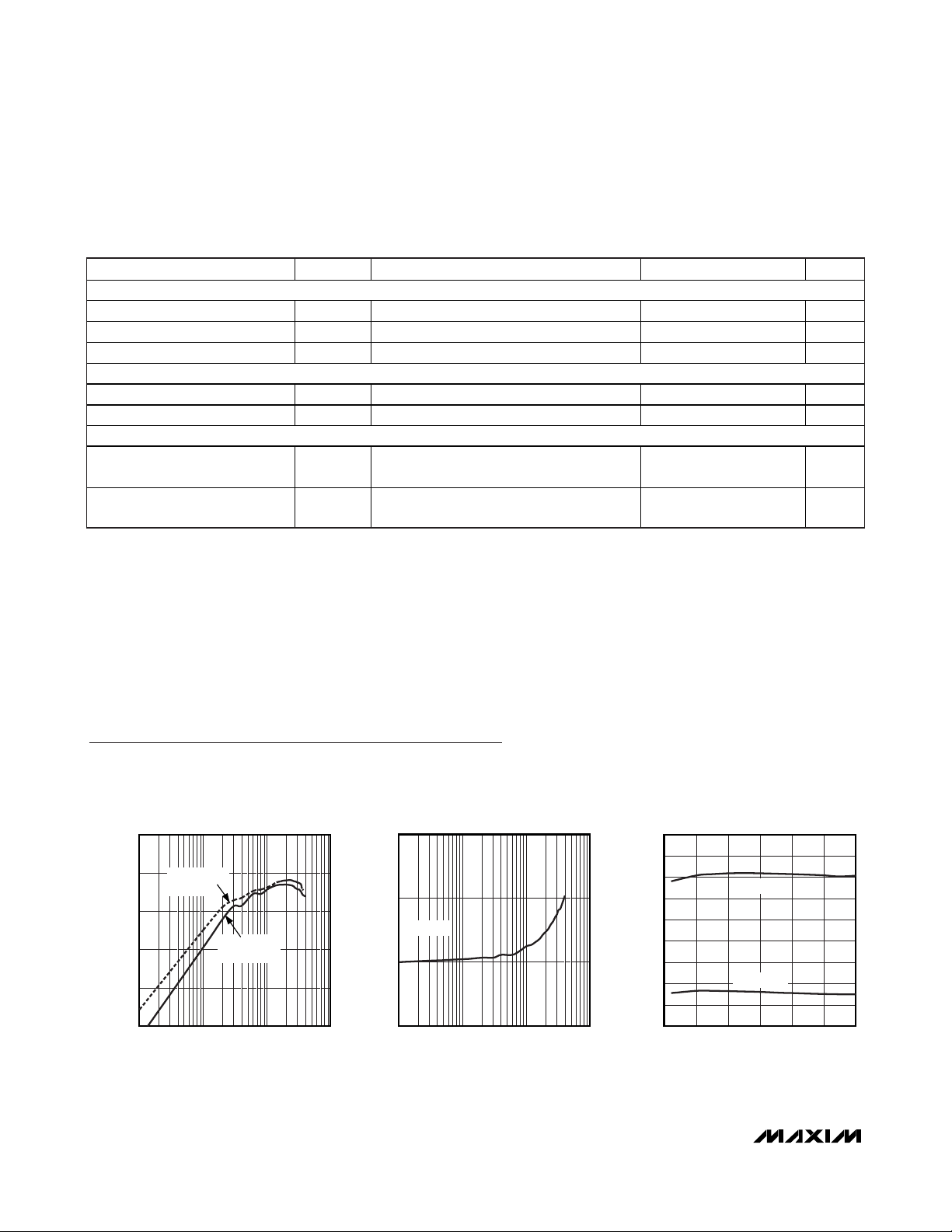
Typical Operating Characteristics
(Circuit of Figure 1, VIN= 3.3V, f
EFFICIENCY vs. L0AD CURRENT
100
90
80
70
EFFICIENCY (%)
60
50
1 100010010
IN
f
= 640kHz
OSC
= 4.7μH
L
LOAD CURRENT (mA)
f
OSC
= 3.3μH
L
OUT
= 1.2MHz
(V
= 3.3V, V
4 _______________________________________________________________________________________
= 640kHz, TA= +25°C, unless otherwise noted.)
OSC
STEP-UP CONVERTER
= 9V)
MAX17067 toc01
0.5
REGULATION (%)
-0.5
1.0
0
1 100010010
LOAD REGULATION
L = 3.3μH
LOAD CURRENT (mA)
1400
1300
MAX17067 toc02
1200
1100
1000
900
800
SWITCHING FREQUENCY (kHz)
700
600
500
2.5 5.54.53.5 5.04.03.0
SWITCHING FREQUENCY
vs. INPUT VOLTAGE
INPUT VOLTAGE (V)
FREQ = IN
MAX17067 toc03
FREQ = GND
Page 5

MAX17067
Low-Noise Step-Up DC-DC Converter
_______________________________________________________________________________________
5
Typical Operating Characteristics (continued)
(Circuit of Figure 1, VIN= 3.3V, f
OSC
= 640kHz, TA= +25°C, unless otherwise noted.)
LX
5V/div
INDUCTOR
CURRENT
1A/div
0V
0A
1μs/div
SWITCHING WAVEFORMS
(I
LOAD
= 500mA)
MAX17067 toc08
vs. SUPPLY VOLTAGE
4.0
3.5
3.0
2.5
2.0
1.5
SUPPLY CURRENT (mA)
1.0
0.5
0
2.5 2.9 3.1 3.32.7 3.5 3.7 3.9
LOAD-TRANSIENT RESPONSE
(I
LOAD
SUPPLY CURRENT
MAX17067 toc04
SWITCHING
NONSWITCHING
SUPPLY VOLTAGE (V)
= 10mA TO 200mA)
MAX17067 toc06
I
OUT
200mA/div
10mA
V
OUT
500mA/div
AC-COUPLED
0V
SOFT-START
(R
= 18Ω)
LOAD
2ms/div
MAX17067 toc05
PULSED LOAD-TRANSIENT RESPONSE
(I
= 40mA TO 1.1A)
LOAD
MAX17067 toc07
V
OUT
5V/div
0V
INDUCTOR
CURRENT
1A/div
0A
I
OUT
1A/div
0.1A
9V
V
OUT
200mV/div
AC-COUPLED
0V
INDUCTOR
CURRENT
500mA/div
100μs/div
L = 3.3μH
= 39kΩ
R
COMP
= 620pF
C
COMP1
0A
10μs/div
L = 3.3μH
= 39kΩ
R
COMP
= 620pF
C
COMP1
INDUCTOR
CURRENT
1A/div
0A
Page 6

MAX17067
Low-Noise Step-Up DC-DC Converter
6 _______________________________________________________________________________________
Pin Description
Switch Pin. Connect the inductor/catch diode to LX and minimize the trace area for lowest EMI.LX5
Supply Pin. Bypass IN with at least a 1μF ceramic capacitor directly to GND.IN6
Frequency Select Input. When FREQ is low, the oscillator frequency is set to 640kHz. When FREQ is high,
the frequency is 1.2MHz. This input has a 5μA pulldown current.
FREQ7
Soft-Start Control Pin. Connect a soft-start capacitor (CSS) to this pin. Leave open for no soft-start. The softstart capacitor is charged with a constant current of 4μA. Full current limit is reached after t = 2.5
x 10
5
CSS.
The soft-start capacitor is discharged to ground when SHDN is low. When SHDN goes high, the soft-start
capacitor is charged to 0.5V, after which soft-start begins.
SS8
GroundGND4
Active-Low Shutdown Control Input. Drive SHDN low to turn off the MAX17067. SHDN
3
PIN
Feedback Pin. Reference voltage is 1.24V nominal. Connect an external resistor-divider tap to FB and
minimize the trace area. Set V
OUT
according to: V
OUT
= 1.24V (1 + R1 / R2). See Figure 1.
FB2
Compensation Pin for Error Amplifier. Connect a series RC from COMP to ground. See the
Loop
Compensation
section for component selection guidelines.
COMP1
FUNCTIONNAME
Detailed Description
The MAX17067 is a highly efficient power supply that
employs a current-mode, fixed-frequency PWM architecture for fast-transient response and low-noise operation.
The device regulates the output voltage through a combination of an error amplifier, two comparators, and several signal generators (Figure 2). The error amplifier
compares the signal at FB to 1.24V and varies the
COMP output. The voltage at COMP determines the current trip point each time the internal MOSFET turns on.
As the load varies, the error amplifier sources or sinks
current to the COMP output accordingly to produce the
inductor peak current necessary to service the load. To
maintain stability at high duty cycle, a slope-compensation signal is summed with the current-sense signal.
At light loads, this architecture allows the ICs to “skip”
cycles to prevent overcharging the output voltage. In
this region of operation, the inductor ramps up to a fixed
peak value, discharges to the output, and waits until
another pulse is needed again.
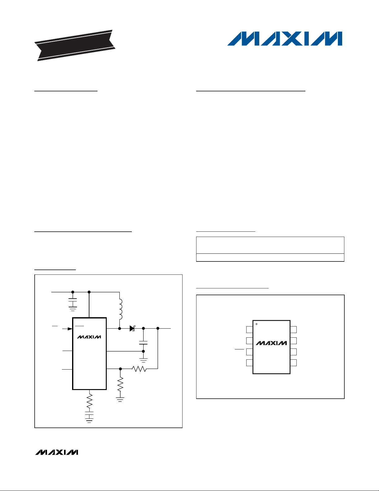
Figure 1. Typical Application Circuit
C
V
2.6V TO 4.0V
ON/OFF
1.2MHz
640kHz
0.027μF
IN
IN
V
IN
C
COMP2
C1
10μF
6.3V
SHDN
MAX17067
FREQ
SS
IN
COMP
GND
R
C
LX
FB
COMP
COMP
L
V
OUT
D1
MBRS130LT1
C
OUT
R1
R2
Page 7

MAX17067
Low-Noise Step-Up DC-DC Converter
_______________________________________________________________________________________ 7
IN Supply Clamp Circuit
The MAX17067 features an internal clamp to allow applications where there is overvoltage stress on the supply
line. In many cases, high-voltage spikes happen on production lines and are difficult to protect against. The
MAX17067’s internal clamp circuit can solve this problem. The internal clamp circuit limits the voltage at the IN
pin to 6.4V (typ) to protect the IN pin from a continuous
or transient overvoltage stress condition on the supply
line. To use the clamp circuit, put a series resistor (RIN)
between supply and IN, and a decoupling capacitor
(1μF typical) from IN to GND. To properly size the external resistor, several factors should be considered:
• The maximum current for the clamp is 40mA, and the
clamp voltage at the IN pin is 6.05V (min). Therefore,
the external resistor is:
• Power dissipation in the clamp is in addition to the
total power loss.
• The external resistor causes a DC voltage drop in
the IN supply line. The voltage at the IN pin has to
be properly maintained when clamping is used. The
worst-case quiescent current of the IN pin is 2.5mA;
therefore, the worst-case voltage drop is 2.5mA
multiplied by R
IN
.
Output-Current Capability
The output-current capability of the MAX17067 is a
function of current limit, input voltage, operating frequency, and inductor value. Because of the slope compensation used to stabilize the feedback loop, the duty
cycle affects the current limit. The output-current capability is governed by the following equation:
I
OUT(MAX)
= [I
LIM
x (1.26 - 0.4 x Duty) -
0.5 x Duty x VIN/(f
OSC
x L)] x η x VIN/V
OUT
where:
I
LIM
= current limit specified at 68% (see the
Electrical
Characteristics
):
Duty = duty cycle = (V
OUT
- VIN+ V
DIODE
)/
(V
OUT
- I
LIM
x RON+ V
DIODE
)
V
DIODE
= catch diode forward voltage at I
LIM
η = conversion efficiency, 85% nominal
RV
IN IN
≥
()
⎡
⎣
⎤
⎦
-605 004..Ω
Figure 2. Functional Diagram
SHDN
BIAS
COMP
ERROR
AMPLIFIER
FB
∞
1.24V
SLOPE
FREQ
OSCILLATOR
5μA
COMPEN-
SATION
Σ
SKIP
COMPARATOR
ERROR
COMPARATOR
CLOCK
SKIP
CONTROL
AND DRIVER
LOGIC
CURRENT
SENSE
4μA
SOFTSTART
N
MAX17067
IN
SS
LX
GND
Page 8
MAX17067MAX17067
Low-Noise Step-Up DC-DC Converter
8 _______________________________________________________________________________________
Soft-Start
The MAX17067 can be programmed for soft-start upon
power-up with an external capacitor. When the shutdown pin is taken high, the soft-start capacitor (CSS) is
immediately charged to 0.5V. Then the capacitor is
charged at a constant current of 4.5μA (typ). During
this time, the SS voltage directly controls the peak
inductor current, allowing 0A at V
SS
= 0.5V to the full
current limit at VSS= 1.5V. The maximum load current
is available after the soft-start cycle is completed.
When the shutdown pin is taken low, the soft-start
capacitor is discharged to ground.
Frequency Selection
The MAX17067’s frequency can be user selected to operate at either 640kHz or 1.2MHz. Connect FREQ to GND
for 640kHz operation. For a 1.2MHz switching frequency, connect FREQ to IN. This allows the use of small,
minimum-height external components while maintaining
low output noise. FREQ has an internal pulldown, allowing the user the option of leaving FREQ unconnected
for 640kHz operation.
Shutdown
The MAX17067 is shut down to reduce the supply current to 30μA when SHDN is low. In this mode, the internal reference, error amplifier, comparators, and biasing
circuitry turn off while the n-channel MOSFET is turned
off. The boost converter’s output is connected to IN by
the external inductor and catch diode.
Thermal-Overload Protection
Thermal-overload protection prevents excessive power
dissipation from overheating the MAX17067. When the
junction temperature exceeds TJ= +160°C, a thermal
sensor immediately activates the fault protection, which
shuts down the MAX17067, allowing the device to cool
down. Once the device cools down by approximately
20°C, it returns to normal operation.
Applications Information
Boost DC-DC converters using the MAX17067 can be
designed by performing simple calculations for a first
iteration. All designs should be prototyped and tested
prior to production. Table 1 provides a list of components for a range of standard applications. Table 2 lists
component suppliers.
External component value choice is primarily dictated
by the output voltage and the maximum load current,
as well as maximum and minimum input voltages.
Begin by selecting an inductor value. Once L is known,
choose the diode and capacitors.
Inductor Selection
The minimum inductance value, peak current rating, and
series resistance are factors to consider when selecting
the inductor. These factors influence the converter’s efficiency, maximum output load capability, transientresponse time, and output voltage ripple. Physical size
and cost are also important factors to be considered.
Table 2. Component Suppliers
847-639-6400
561-241-7876
847-956-0666
PHONE
847-639-1469Coilcraft
561-241-9339Coiltronics
847-956-0702Sumida USA
FAXSUPPLIER
803-946-0690
408-986-0424
619-661-6835
847-297-0070
803-626-3123AVX
408-986-1442KEMET
619-661-1055SANYO
847-699-1194TOKO
408-573-4150 408-573-4159Taiyo Yuden
Inductors
Capacitors
PHONE FAXSUPPLIER
516-435-1110
310-322-3331
516-543-7100
602-303-5454
847-843-7500
516-864-7630Zetex
847-843-2798Nihon
516-435-1824
Central
Semiconductor
310-322-3332
International
Rectifier
602-994-6430Motorola
Diodes
Table 1. Component Selection
C
VIN (V) V
3.3 9 1.2M 3.3 10 121 620 10 250
3.3 9 640k 4.7 10 82 1000 10 250
OUT
(V) f
(Hz) L (μH) C
OSC
OUT
(μF) R
COMP
(k ) C
COMP
(pF)
COMP 2
(pF)
I
OUT(MAX)
(mA)
Page 9

MAX17067
Low-Noise Step-Up DC-DC Converter
_______________________________________________________________________________________ 9
The maximum output current, input voltage, output voltage, and switching frequency determine the inductor
value. Very high inductance values minimize the current ripple and therefore reduce the peak current,
which decreases core losses in the inductor and I2R
losses in the entire power path. However, large inductor values also require more energy storage and more
turns of wire, which increase physical size and can
increase I2R losses in the inductor. Low inductance values decrease the physical size but increase the current
ripple and peak current. Finding the best inductor
involves choosing the best compromise between circuit
efficiency, inductor size, and cost.
The equations used here include a constant LIR, which
is the ratio of the inductor peak-to-peak ripple current to
the average DC inductor current at the full load current.
The best trade-off between inductor size and circuit
efficiency for step-up regulators generally has an LIR
between 0.3 and 0.5. However, depending on the AC
characteristics of the inductor core material and the
ratio of inductor resistance to other power path resistances, the best LIR can shift up or down. If the inductor resistance is relatively high, more ripple can be
accepted to reduce the number of turns required and
increase the wire diameter. If the inductor resistance is
relatively low, increasing inductance to lower the peak
current can decrease losses throughout the power
path. If extremely thin high-resistance inductors are
used, as is common for LCD-panel applications, the
best LIR can increase to between 0.5 and 1.0.
Once a physical inductor is chosen, higher and lower
values of the inductor should be evaluated for efficiency
improvements in typical operating regions.
Calculate the approximate inductor value using the typical input voltage (VIN), the maximum output current
(I
MAIN(MAX)
), the expected efficiency (η
TYP
) taken from
an appropriate curve in the
Typical Operating
Characteristics
, and an estimate of LIR based on the
above discussion:
Choose an available inductor value from an appropriate
inductor family. Calculate the maximum DC input current at the minimum input voltage V
IN(MIN)
using con-
servation of energy and the expected efficiency at that
operating point (η
MIN
) taken from an appropriate curve
in the
Typical Operating Characteristics
:
Calculate the ripple current at that operating point and
the peak current required for the inductor:
The inductor’s saturation current rating and the
MAX17067s’ LX current limit (I
LIM
) should exceed I
PEAK
and the inductor’s DC current rating should exceed
I
IN(DC,MAX)
. For good efficiency, choose an inductor with
less than 0.1Ω series resistance.
Considering the application circuit in
Figure 4, the maxi-
mum load current (I
MAIN(MAX)
) is 250mA with a 9V output
and a typical input voltage of 3.3V. Choosing an LIR of 0.7
and estimating efficiency of 85% at this operating point:
Using the application’s minimum input voltage (3V) and
estimating efficiency of 80% at that operating point:
The ripple current and the peak current are:
2
IN
⎛
⎞
⎟
⎠
VV
MAIN IN
⎜
I f LIR
()
MAIN MAX OSC
⎝
⎛
V
L
=
⎜
V
⎝
MAIN
⎞
−
×
η
⎛
⎞
TYP
⎜
⎟
⎠
⎟
⎝
⎠
I
IN DC MAX
(, )
IV
MAIN MAX MAIN
=
V
IN MIN MIN
×
()
×η
()
VVV
I
RIPPLE
II
IN MIN MAIN IN MIN
=
=+
PEAK IN DC MAX
×−
() ()
()
LV f
××
MAIN OSC
I
(, )
RIPPLE
2
⎛
L
=
⎜
⎝
2
..
33
9
V
⎞
⎟
⎠
V
VV
−
933
⎛
⎜
⎝
..
AMHz
×
025 12
. 55
08
⎛
⎞
⎜
⎟
⎝
⎠
0733.
⎞
≈μH
⎟
⎠
.
I
IN DC MAX(, )
AV
.
×
308
V
≈
.=
094
A
.
×
025 9
VVV
×−
393
I
=
RI PPLE
33 9 12
IAAA
PEAK
()
HV MHz
××
..
μ
051
=+≈094
.
2
≈
051
.
119.
.
A
Page 10

MAX17067
Low-Noise Step-Up DC-DC Converter
10 ______________________________________________________________________________________
Diode Selection
The output diode should be rated to handle the output
voltage and the peak switch current. Make sure that the
diode’s peak current rating is at least IPKand that its
breakdown voltage exceeds V
OUT
. Schottky diodes are
recommended.
Input and Output Capacitor Selection
Low-ESR capacitors are recommended for input
bypassing and output filtering. Low-ESR tantalum
capacitors are a good compromise between cost and
performance. Ceramic capacitors are also a good
choice. Avoid standard aluminum electrolytic capacitors. A simple equation to estimate input and outputcapacitor values for a given voltage ripple is as follows:
where V
RIPPLE
is the peak-to-peak ripple voltage on the
capacitor.
Output Voltage
The MAX17067 operates with an adjustable output from
VINto 20V. Connect a resistor voltage-divider to FB
(see the
Typical Operating Circuit
) from the output to
GND. Select the resistor values as follows:
where VFB, the boost-regulator feedback set point, is
1.24V. Since the input bias current into FB is typically
zero, R2 can have a value up to 100kΩ without sacrificing
accuracy. Connect the resistor-divider as close to the IC
as possible.
Loop Compensation
The voltage feedback loop needs proper compensation
to prevent excessive output ripple and poor efficiency
caused by instability. This is done by connecting a resistor (R
COMP
) and capacitor (C
COMP
) in series from
COMP to GND, and another capacitor (C
COMP2
) from
COMP to GND. R
COMP
is chosen to set the high-frequency integrator gain for fast-transient response, while
C
COMP
is chosen to set the integrator zero to maintain
loop stability. The second capacitor, C
COMP2
, is chosen
to cancel the zero introduced by output-capacitance
ESR. For optimal performance, choose the components
using the following equations:
R
COMP
= (274Ω/A2x
V
IN
x
V
OUT
x C
OUT
/(L x I
OUT
)
C
COMP
≅ (0.36 x 10⁻³A/Ω) x L/V
IN
C
COMP2
≅ (0.0036 A/Ω) x R
ESR
x L x I
OUT
/(V
IN
x
V
OUT
)
For the ceramic output capacitor, where ESR is small,
C
COMP2
is optional. Table 1 shows experimentally verified
external component values for several applications.
The best gauge of correct loop compensation is by
inspecting the transient response of the MAX17067.
Adjust R
COMP
and C
COMP
as necessary to obtain opti-
mal transient performance.
Soft-Start Capacitor
The soft-start capacitor should be large enough that it
does not reach final value before the output has
reached regulation. Calculate CSSto be:
where:
C
OUT
= total output capacitance including any bypass
capacitor on the output bus
V
OUT
= maximum output voltage
I
INRUSH
= peak inrush current allowed
I
OUT
= maximum output current during power-up stage
VIN= minimum input voltage
The load must wait for the soft-start cycle to finish
before drawing a significant amount of load current.
The duration after which the load can begin to draw
maximum load current is:
t
MAX
= 2.5 x 10⁵C
SS
C 21 10 C
V
V V
V I I V
SS
6
OUT
IN OUT
IN INRUSH OUT OUT
OUT
2
>× ×
−×
×−×
⎛
⎝
⎜
⎞
⎠
⎟
−
RR
V
V
OUT
FB
12 1=−
⎛
⎝
⎜
⎞
⎠
⎟
C
0.5 L I
V V
PK
2
RIPPLE OUT
≥
××
⎛
⎝
⎞
⎠
×
Page 11

MAX17067
Low-Noise Step-Up DC-DC Converter
______________________________________________________________________________________ 11
Application Circuits
1-Cell to 3.3V SEPIC Power Supply
Figure 3 shows the MAX17067 in a single-ended primary
inductance converter (SEPIC) topology. This topology is
useful when the input voltage can be either higher or
lower than the output voltage, such as when converting
a single lithium-ion (Li+) cell to a 3.3V output. L1A and
L1B are two windings on a single inductor. The coupling
capacitor between these two windings must be a lowESR type to achieve maximum efficiency, and must also
be able to handle high ripple currents. Ceramic capacitors are best for this application. The circuit in Figure 3
provides 400mA output current at 3.3V output when
operating with an input voltage from +2.6V to +4.0V.
AMLCD Application
Figure 4 shows a power supply for active matrix (TFTLCD) flat-panel displays. Output-voltage transient performance is a function of the load characteristic. Add or
remove output capacitance (and recalculate compensation-network component values) as necessary to
meet transient performance. Regulation performance
for secondary outputs (VGOFF and VGON) depends on
the load characteristics of all three outputs.
Figure 4. Multiple-Output, Low-Profile (1.2mm max) TFT-LCD Power Supply
Figure 3. MAX17067 in a SEPIC Configuration
D4 D2
R6
100kΩ
C15
27nF
1
3
2
L1
3.3μH
6
IN
U1
MAX17067
3
SHDN
7
FREQ
8
SS
COMP
1
R5
121kΩ
C5
620pF
2.6V TO 4.0V
C1
10μF
10V
VGOFF
-9V
C14
4.7μF
V
IN
R3
C4
10Ω
1μF
V
IN
2.6V TO 4.0V
L1A
5.3μH
IN
SHDN
LX
MAX17067
0.027μF
C
COMP2
R
C
FREQ
SS
COMP
COMP
GND
FB
CC
C9
0.1μF
LX
GND
FB
5
4
2
C6
OPEN
C11
0.1μF
C10
0.1μF
D1
2
3
1
C12
D3
3
10μF
25V
R1
274kΩ
R2
44.2kΩ
1μF
2
1
C7
C2
10μF
L1B
5.3μH
R2
605kΩ
L1 = CTX8-1P
C
OUT
C13
1μF
C1
10μF
10V
D1
C
OUT
22μF
20V
R1
1MΩ
= TPSD226025R0200
VGON
+27V
V
OUT
+9V/250mA
V
3.3V
OUT
Page 12

MAX17067
Layout Procedure
Good PCB layout and routing are required in high-frequency switching power supplies to achieve good regulation, high efficiency, and stability. It is strongly
recommended that the evaluation kit PCB layouts be followed as closely as possible. Place power components
as close together as possible, keeping their traces short,
direct, and wide. Avoid interconnecting the ground pins
of the power components using vias through an internal
ground plane. Instead, keep the power components
close together and route them in a star ground configuration using component-side copper, then connect the star
ground to internal ground using multiple vias.
Low-Noise Step-Up DC-DC Converter
12 ______________________________________________________________________________________
Chip Information
TRANSISTOR COUNT: 3657
Page 13
MAX17067
Low-Noise Step-Up DC-DC Converter
MAX17067
Maxim cannot assume responsibility for use of any circuitry other than circuitry entirely embodied in a Maxim product. No circuit patent licenses are
implied. Maxim reserves the right to change the circuitry and specifications without notice at any time.
13
____________________Maxim Integrated Products, 120 San Gabriel Drive, Sunnyvale, CA 94086 408-737-7600
© 2008 Maxim Integrated Products is a registered trademark of Maxim Integrated Products, Inc.
Package Information
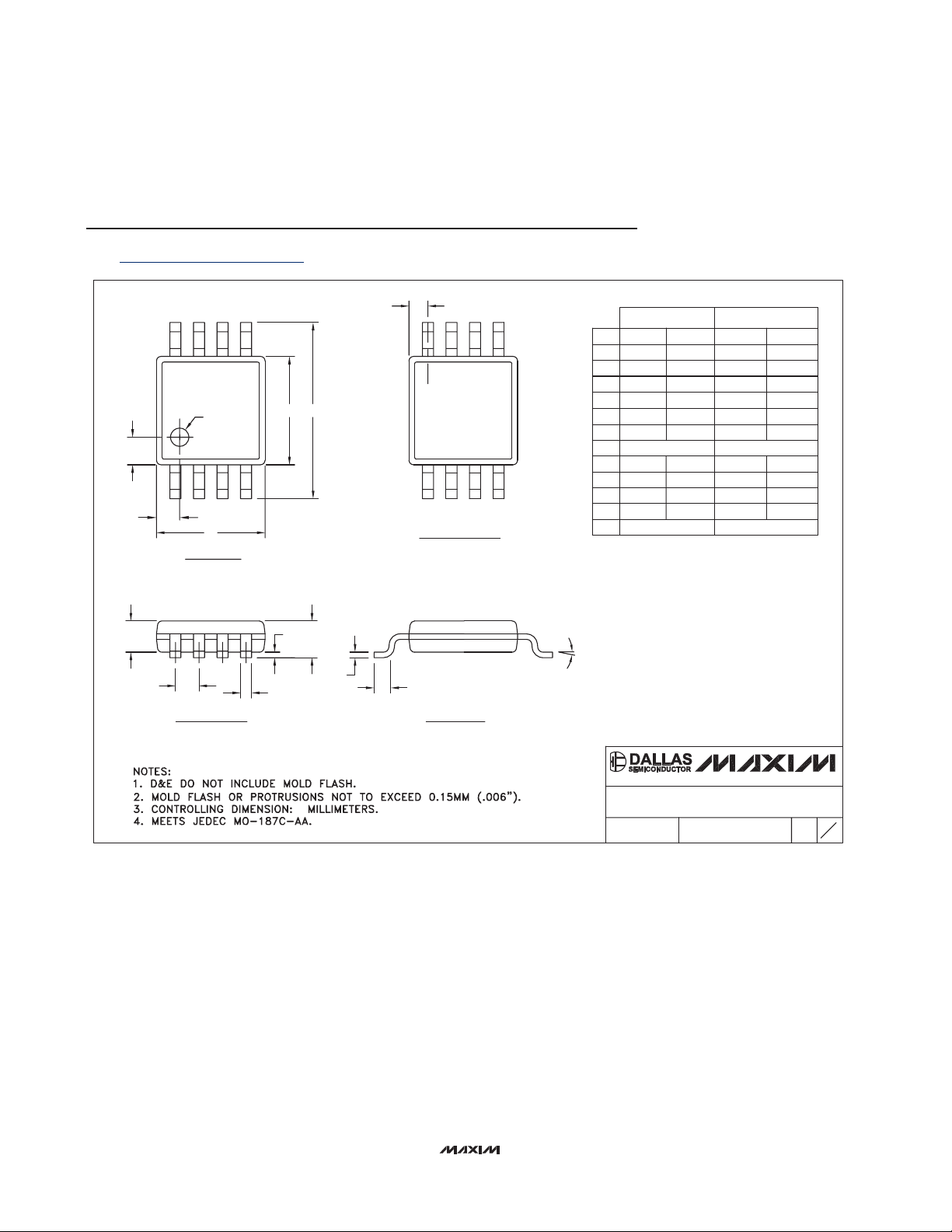
(The package drawing(s) in this data sheet may not reflect the most current specifications. For the latest package outline information,
go to www.maxim-ic.com/packages
.)
8
Ø0.50±0.1
0.6±0.1
0.6±0.1
1
D
TOP VIEW
A2
E H
A1
4X S
BOTTOM VIEW
A
8
1
DIM
A
A1
A2
b
c
D
e
E
H
L
α
S
INCHES
MIN
-
0.002
0.030
0.010
0.005
0.116
0.0256 BSC
0.116
0.188
0.016
0°
0.0207 BSC
MAX
0.043
0.006
0.037
0.014
0.007
0.120
0.120
0.198
0.026
6°
MILLIMETERS
MIN
0.05 0.15
0.25 0.36
0.13 0.18
2.95 3.05
2.95 3.05
4.78
0.41
MAX
- 1.10
0.950.75
0.65 BSC
5.03
0.66
6°0°
0.5250 BSC
8LUMAXD.EPS
e
FRONT VIEW
c
b
L
SIDE VIEW
α
PROPRIETARY INFORMATION
TITLE:
PACKAGE OUTLINE, 8L uMAX/uSOP
REV.DOCUMENT CONTROL NO.APPROVAL
21-0036
1
J
1
 Loading...