

Page 1
General Description
The MAX17062 is a high-performance step-up DC-DC
converter that provides a regulated supply voltage for
active-matrix thin-film transistor (TFT) liquid-crystal displays (LCDs). The MAX17062 incorporates currentmode, fixed-frequency, pulse-width modulation (PWM)
circuitry with a built-in n-channel power MOSFET to
achieve high efficiency and fast-transient response.
Users can select 640kHz or 1.2MHz operation using a
logic input pin (FREQ). The high switching frequencies
allow the use of ultra-small inductors and low-ESR
ceramic capacitors. The current-mode architecture provides fast transient response to pulsed loads. A compensation pin (COMP) gives users flexibility in adjusting
loop dynamics. The 22V internal MOSFET can generate
output voltages up to 20V from an input voltage
between 2.6V and 5.5V. Soft-start slowly ramps the input
current and is programmed with an external capacitor.
The MAX17062 is available in a 10-pin TDFN package.
Applications
Notebook Computer Displays
LCD Monitor Panels
LCD TV Panels
Features
o 90% Efficiency
o Adjustable Output from V
IN
to 20V
o 2.6V to 5.5V Input Supply Range
o Input Supply Undervoltage Lockout
o Pin-Programmable 640kHz/1.2MHz Switching
Frequency
o Programmable Soft-Start
o Improved EMI
o FB Regulation Voltage Tolerance < 1%
o Small 10-Pin TDFN Package
o Thermal-Overload Protection
MAX17062
TFT-LCD Step-Up DC-DC Converter
________________________________________________________________
Maxim Integrated Products
1
Ordering Information
19-1042; Rev 0; 10/07
For pricing, delivery, and ordering information, please contact Maxim Direct at 1-888-629-4642,
or visit Maxim’s website at www.maxim-ic.com.
EVALUATION KIT
AVAILABLE
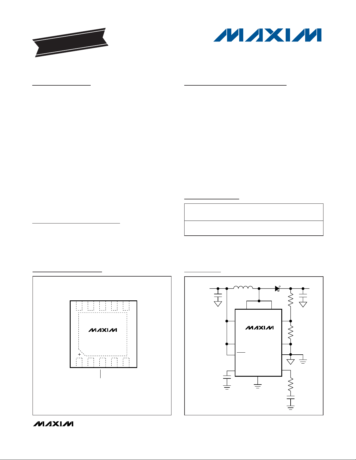
Pin Configuration
LX LX
FB
PGND
PGND
AGND
FREQ
IN
COMP
SS
EP
1
4
5
2
3
9
8
67
10
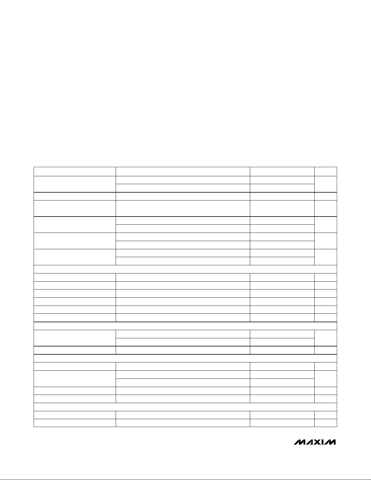
V
OUT
V
IN
2.6V TO 5.5V
SHDN
MAX17062
Minimal Operating Circuit
+
Denotes a lead-free package.
*
EP = Exposed pad.
T = Tape and reel.
PART TEMP RANGE
MAX17062ETB+T -40°C to +85°C
PINPACKAGE
10 TDFN-EP*
(3mm x 3mm)
PKG
CODE
T1033-2
SS
TOP VIEW
*EP = EXPOSED PAD.
FREQ
10 9 8 7 6
MAX17062
12345
FB
COMP
TDFN
(3mm x 3mm)
LX
*EP
PGND
LX
PGND
IN
SHDN
Page 2
MAX17062
TFT-LCD Step-Up DC-DC Converter
2 _______________________________________________________________________________________
ABSOLUTE MAXIMUM RATINGS
ELECTRICAL CHARACTERISTICS
(VIN= V
SHDN
= 3V, FREQ = 3V, TA= 0°C to +85°C. Typical values are at TA= +25°C, unless otherwise noted.) (Note 1)
Stresses beyond those listed under “Absolute Maximum Ratings” may cause permanent damage to the device. These are stress ratings only, and functional
operation of the device at these or any other conditions beyond those indicated in the operational sections of the specifications is not implied. Exposure to
absolute maximum rating conditions for extended periods may affect device reliability.
LX to AGND ............................................................-0.3V to +22V
IN, SHDN, FREQ, FB to AGND..............................-0.3V to +7.5V
COMP, SS to AGND ....................................-0.3V to (V
IN
+ 0.3V)
PGND to AGND .....................................................-0.3V to +0.3V
LX Switch Maximum Continuous RMS Current .....................3.2A
Continuous Power Dissipation (T
A
= +70°C)
10-Pin TDFN (derate 24.4mW/°C above +70°C)..........1951mW
Operating Temperature Range ...........................-40°C to +85°C
Junction Temperature......................................................+150°C
Storage Temperature Range .............................-65°C to +160°C
Lead Temperature (soldering, 10s) .................................+300°C
Input Voltage Range
Output Voltage Range 20 V
IN Undervoltage-Lockout
Threshold
IN Quie scent Current
IN Shutdown Current
Thermal Shutdown
ERROR AMPLIFIER
FB Regulation Voltage Level to produce V
FB Input Bia s Current VFB = 1.24V 75 150 225 nA
FB L ine Regulation Level to produce V
Transconductance 110 250 450 μS
Voltage Gain 2400 V/V
Shutdown FB Input Voltage SHDN = AGND 0.05 0.10 0.15 V
OSCILLATOR
Frequency
Max imum Duty C yc le 88 91 94 %
n-CHANNEL MOSFET
Current Lim it VFB = 1V, 75% duty cycle, IN = 5V 3.9 4.6 5.3 A
On-Resistance
Leakage Current VLX = 20V 11 20 μA
Current-Sense Tran sresi stance IN = 5V 0.09 0.15 0.25 V/A
SOFT-START
Reset Switch Re sistance 100
Charge Current VSS = 1.2V 2 4 6 μA
PARAMETER CONDITIONS MIN TYP MA X UNITS
V
< 18V 2.6 5.5
OUT
18V < V
V
VFB = 1.3V, not switching 0.3 0.6
V
SHDN = AGND, TA = +25°C 0.01 10.0
SHDN = AGND, T
Temperature ris ing 160
Hysteresis 20
FREQ = AGND 500 640 780
FREQ = IN 1000 1200 1400
IN = 5V 100 170
IN = 3V 125 210
OUT
rising, typical hysteresis i s 50mV 2.30 2.45 2.57 V
IN
= 1.0V, switching 1.5 2.5
FB
< 20V 4.0 5.5
= +85°C 0.01
A
COMP
COMP
= 1.24V 1.23 1.24 1.25 V
= 1.24V, VIN = 2.6V to 5.5V 0.01 0.15 %/V
V
mA
μA
°C
kHz
m
Page 3
MAX17062
TFT-LCD Step-Up DC-DC Converter
_______________________________________________________________________________________ 3
ELECTRICAL CHARACTERISTICS (continued)
(VIN= V
SHDN
= 3V, FREQ = 3V, TA= 0°C to +85°C. Typical values are at TA= +25°C, unless otherwise noted.) (Note 1)
ELECTRICAL CHARACTERISTICS
(VIN= V
SHDN
= 3V, FREQ = 3V, TA= -40°C to +85°C, unless otherwise noted.) (Note 1)
CONTROL I NPU TS
SHDN, FREQ Input Low Voltage VIN = 2.6V to 5.5V
SHDN, FREQ Input High Voltage VIN = 2.6V to 5.5V
SHDN, FREQ Input Hysteresis VIN = 2.6V to 5.5V
FREQ Pulldown Current 3 6 9 μA
SHDN Input Current
PARAMETER CONDITIONS MIN TYP MA X UNITS
0.3
V
IN
0.7
V
IN
SHDN = AGND, TA = +25°C -1 +1
SHDN = AGND, T
= +85°C 0
A
V
0.1
V
IN
V
V
μA
Input Voltage Range
Output Voltage Range 20 V
IN Undervoltage-Lockout
Threshold
IN Quie scent Current
ERROR AMPLIFIER
FB Regulation Voltage Level to produce V
FB Input Bia s Current VFB = 1.24V 225 nA
FB L ine Regulation Level to produce V
Transconductance 110 450 μS
Shutdown FB Input Voltage SHDN = AGND 0.05 0.15 V
OSCILLATOR
Frequency
Maximum Duty Cycle 87 95 %
n-CHANNEL MOSFET
Current Lim it VFB = 1V, 75% duty c ycle, IN = 5V 3.9 5.3 A
On-Resistance
Current-Sense Tran sresi stance IN = 5V 0.09 0.25 V/A
SOFT-START
Reset Switch Re sistance 100
Charge Current VSS = 1.2V 2 6 μA
PARAMETER CONDITIONS MIN TY P MAX UNITS
V
< 18V 2.6 5.5
OUT
18V < V
V
rising, typical hysteresis i s 50mV 2.30 2.57 V
IN
VFB = 1.3V, not switching 0.6
= 1.0V, switching 2.5
V
FB
FREQ = AGND 450 830
FREQ = IN 950 1500
IN = 5V 170
IN = 3V 210
< 20V 4.0 5.5
OUT
= 1.24V 1.227 1.253 V
COMP
= 1.24V, VIN = 2.6V to 5.5V 0.15 %/V
COMP
V
mA
kHz
m
Page 4
MAX17062
TFT-LCD Step-Up DC-DC Converter
4 _______________________________________________________________________________________
Note 1: Limits are 100% tested at TA= +25°C. Maximum and minimum limits over temperature are guaranteed by design.
ELECTRICAL CHARACTERISTICS (continued)
(VIN= V
SHDN
= 3V, FREQ = 3V, TA= -40°C to +85°C, unless otherwise noted.) (Note 1)
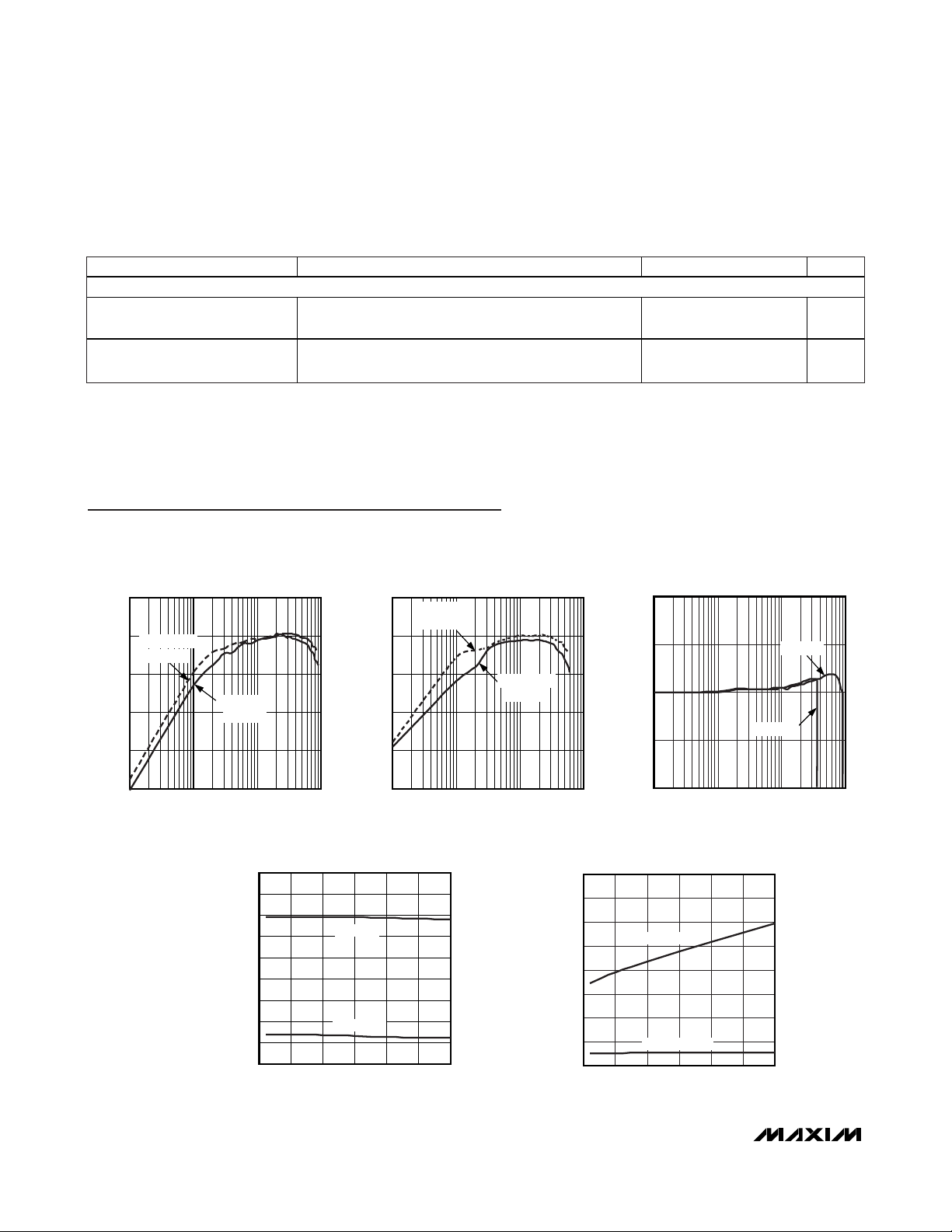
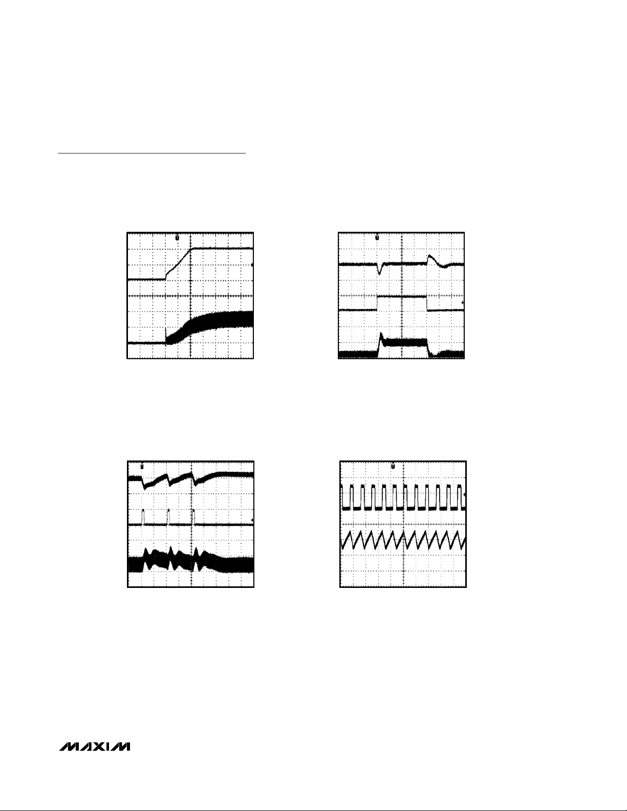
Typical Operating Characteristics
(Circuit of Figure 1. VIN= 5V, V
MAIN
= 15V, TA= +25°C, unless otherwise noted.)
CONTROL I NPU TS
SHDN, FREQ Input Low Voltage VIN = 2.6V to 5.5V
SHDN, FREQ Input High Voltage VIN = 2.6V to 5.5V
PARAMETER CONDITIONS MIN TY P MAX UNITS
0.7
V
IN
V
0.3
V
IN
V
EFFICIENCY vs. LOAD CURRENT
= 5V, V
(V
f
= 640kHz
OSC
L = 4.7μH
IN
LOAD CURRENT (mA)
100
90
80
70
EFFICIENCY (%)
60
50
1 1000
= 15V)
OUT
f
= 1.2MHz
OSC
L = 2.7μH
10010
1400
1300
1200
1100
1000
900
800
SWITCHING FREQUENCY (kHz)
700
600
500
2.5 5.5
100
MAX17062 toc01
90
80
70
EFFICIENCY (%)
60
50
1 1000
SWITCHING FREQUENCY
vs. INPUT VOLTAGE
FREQ = IN
FREQ = GND
INPUT VOLTAGE (V)
EFFICIENCY vs. LOAD CURRENT
(V
IN
f
= 640kHz
OSC
L = 4.7μH
LOAD CURRENT (mA)
5.04.54.03.53.0
= 3.3V, V
MAX17062 toc04
= 9V)
OUT
f
= 1.2MHz
OSC
L = 2.7μH
10010
SUPPLY CURRENT (mA)
LOAD REGULATION
(V
1.0
MAX17062 toc02
0.5
0
LOAD REGULATION (%)
-0.5
-1.0
1 1000
OUT
LOAD CURRENT (mA)
SUPPLY CURRENT
vs. SUPPLY VOLTAGE
4.0
3.5
3.0
2.5
2.0
1.5
1.0
0.5
0
2.5 5.5
SWITCHING
NONSWITCHING
SUPPLY VOLTAGE (V)
= 15V)
5.04.54.03.53.0
VIN = 5.0V
VIN = 3.3V
10010
MAX17062 toc05
MAX17062 toc03
Page 5
MAX17062
TFT-LCD Step-Up DC-DC Converter
_______________________________________________________________________________________
5
Typical Operating Characteristics (continued)
(Circuit of Figure 1. VIN= 5V, V
MAIN
= 15V, TA= +25°C, unless otherwise noted.)
SOFT-START
= 30Ω)
(R
LOAD
2ms/div
MAX17062 toc06
PULSED LOAD-TRANSIENT RESPONSE
= 100mA TO 1.1A)
(I
LOAD
MAX17062 toc08
V
OUT
5V/div
OV
INDUCTOR
CURRENT
1A/div
OA
15V
V
OUT
200mV/div
AC-COUPLED
I
OUT
1A/div
0.1A
INDUCTOR
CURRENT
1A/div
0A
LOAD-TRANSIENT RESPONSE
= 50mA TO 550mA)
(I
LOAD
L = 2.7μH
R
COMP
C
COMP1
= 47k
= 560pF
100μs/div
Ω
SWITCHING WAVEFORMS
= 600mA)
(I
LOAD
MAX17062 toc07
MAX17062 toc09
15V
V
OUT
500mV/div
AC-COUPLED
0V
I
OUT
500mA/div
50mA
INDUCTOR
CURRENT
2A/div
0A
LX
10V/div
0V
INDUCTOR
CURRENT
1A/div
0A
L = 2.7μH
R
COMP
C
COMP1
= 47kΩ
= 560pF
10μs/div
1μs/div
Page 6

MAX17062
TFT-LCD Step-Up DC-DC Converter
6 _______________________________________________________________________________________
Pin Description
Figure 1. Typical Operating Circuit
PIN NAME FUNCTION
1 COMP
2 FB
3 SHDN Shutdown Control Input. Drive SHDN low to turn off the MAX17062.
4, 5 PGND Power Ground. Connect pin s 4 and 5 directly together.
6, 7 LX
8 IN Supply Pin. Bypass IN with a minimum 1μF ceramic capac itor directly to AGND.
9 FREQ
10 SS
EP AGND Exposed Pad. Connect to AGND.
Compensation Pin for Error Amplifier. Connect a ser ie s RC from COMP to ground. See the Loop
Compensation section for component selection guidelines.
Feedback Pin. The FB regulation voltage is 1.24V nominal. Connect an external resistive voltage-divider
between the step-up regulator’s output (V
) and AGND, with the center tap connected to FB. Place the
OUT
div ider close to the IC and minimize the trace area to reduce noise coupling. Set V
Output Voltage Select ion section.
Switch Pin. LX is the drain of the internal MOSFET. Connect the inductor/rectifier diode junction to LX and
min im ize the trace area for lower EMI. Connect pin s 6 and 7 together.
Frequency-Select Input. When FREQ is low, the oscillator frequency is set to 640kHz. When FREQ is high,
the frequency is 1.2MHz. This input has a 6μA pulldown current.
Soft-Start Control Pin. Connect a soft-start capacitor (C
) to this pin. Leave open for no soft-start. The soft-
SS
start capacitor is charged with a constant current of 4μA. Full current lim it is reached when the voltage of
SS pin is charged to 1.5V, which is the current-lim it time, t = 2.4 10
discharged to ground when SHDN is low. When SHDN goes high, the soft-start capacitor is charged to 0.4V,
after which soft-start begins.
according to the
OUT
5
CSS. The soft- start capacitor is
V
IN
4.5V TO 5.5V
C1
4.7μF
10V
4.7μF
10V
L1
2.7μH
C2
1μF
R1
10Ω
8
C3
IN
MAX17062
3
SHDN
9
FREQ
10
SS
C4
33nF
COMP
1
R2
47kΩ
C5
560pF
PGND
PGND
AGND
C6
OPEN
6
LX
7
LX
5
4
2
FB
EP
D1
C7
10μF
25V
R4
221kΩ
R3
20kΩ
V
OUT
+15V/600mA
C8
10μF
25V
Page 7

Detailed Description
The MAX17062 is a highly efficient power supply that
employs a current-mode, fixed-frequency, PWM architecture for fast-transient response and low-noise operation. The device regulates the output voltage through a
combination of an error amplifier, two comparators, and
several signal generators (Figure 2). The error amplifier
compares the signal at FB to 1.24V and varies the
COMP output. The voltage at COMP determines the
current trip point each time the internal MOSFET turns
on. As the load changes, the error amplifier sources or
sinks current to the COMP output to command the
inductor peak current necessary to service the load. To
maintain stability at high duty cycles, a slope-compensation signal is summed with the current-sense signal.
At light loads, this architecture allows the MAX17062 to
“skip” cycles to prevent overcharging the output voltage.
In this region of operation, the inductor ramps up to a
peak value of approximately 50mA, discharges to the
output, and waits until another pulse is needed again.
Output Current Capability
The output current capability of the MAX17062 is a
function of current limit, input voltage, operating frequency, and inductor value. Because of the slope compensation used to stabilize the feedback loop, the
inductor current limit depends on the duty cycle. The
current limit is determined by the following equation:
I
LIM
= (1.26 - 0.35 x D) x I
LIM_EC
where I
LIM_EC
is the current limit specified at 75% duty
cycle (see the
Electrical Characteristics
table) and D is
the duty cycle.
The output current capability depends on the currentlimit value and is governed by the following equation:
where I
LIM
is the current limit calculated above, η is the
regulator efficiency (85% nominal), and D is the duty
cycle. The duty cycle when operating at the current
limit is:
where V
DIODE
is the rectifier diode forward voltage and
RONis the on-resistance of the internal MOSFET.
MAX17062
TFT-LCD Step-Up DC-DC Converter
_______________________________________________________________________________________ 7
Figure 2. MAX17062 Functional Diagram
SHDN
BIAS
COMP
ERROR
AMPLIFIER
FB
∞
1.24V
SLOPE
FREQ
OSCILLATOR
6μA
COMPEN-
SATION
Σ
SKIP
COMPARATOR
ERROR
COMPARATOR
CLOCK
SKIP
CONTROL
AND DRIVER
LOGIC
CURRENT
SENSE
4μA
SOFTSTART
N
MAX17062
IN
SS
LX
PGND
II
OUT MAX LIM
()
⎢
⎢
⎣
⎡
.
05
DV
××
fLVV
×
OSC
⎤
IN
=−
××
⎥
⎥
⎦
VVV
−+
OUT IN DIODE
VIRV
−× +
OUT LIM ON DIODE
D
=
IN
OUT
η
Page 8

MAX17062
Soft-Start
The MAX17062 can be programmed for soft-start upon
power-up with an external capacitor. When the shutdown
pin is taken high, the soft-start capacitor (CSS) is immediately charged to 0.4V. Then the capacitor is charged at a
constant current of 4μA (typ). During this time, the SS
voltage directly controls the peak inductor current, allowing 0A at VSS= 0.4V to the full current limit at VSS= 1.5V.
The maximum load current is available after the soft-start
is completed. When the SHDN pin is taken low, the softstart capacitor is discharged to ground.
Frequency Selection
The MAX17062’s frequency can be user selected to
operate at either 640kHz or 1.2MHz. Connect FREQ to
AGND for 640kHz operation. For a 1.2MHz switching
frequency, connect FREQ to IN. This allows the use of
small, minimum-height external components while
maintaining low output noise. FREQ has an internal
pulldown, allowing the user the option of leaving FREQ
unconnected for 640kHz operation.
Shutdown
The MAX17062 shuts down to reduce the supply current to 0.01μA when SHDN is low. In this mode, the
internal reference, error amplifier, comparators, and
biasing circuitry turn off, and the n-channel MOSFET is
turned off. The step-up regulator’s output is connected
to IN by the external inductor and rectifier diode.
Thermal-Overload Protection
Thermal-overload protection prevents excessive power
dissipation from overheating the MAX17062. When the
junction temperature exceeds TJ= +160°C, a thermal
sensor immediately activates the fault protection, which
shuts down the MAX17062, allowing the device to cool
down. Once the device cools down by approximately
20°C, the MAX17062 starts up automatically.
Applications Information
Step-up regulators using the MAX17062 can be
designed by performing simple calculations for a first
iteration. All designs should be prototyped and tested
prior to production. Table 1 provides a list of power components for the typical applications circuit (Figure 1).
Table 2 lists component suppliers.
External-component-value choice is primarily dictated
by the output voltage and the maximum load current,
as well as maximum and minimum input voltages.
Begin by selecting an inductor value. Once L is known,
choose the diode and capacitors.
Inductor Selection
The minimum inductance value, peak current rating, and
series resistance are factors to consider when selecting
the inductor. These factors influence the converter’s efficiency, maximum output load capability, transientresponse time, and output-voltage ripple. Physical size
and cost are also important factors to be considered.
The maximum output current, input voltage, output voltage, and switching frequency determine the inductor
value. Very high inductance values minimize the current ripple and therefore reduce the peak current,
which decreases core losses in the inductor and I2R
losses in the entire power path. However, large inductor values also require more energy storage and more
turns of wire, which increase physical size and can
increase I2R losses in the inductor. Low inductance values decrease the physical size but increase the current
ripple and peak current. Finding the best inductor
involves choosing the best compromise between circuit
efficiency, inductor size, and cost.
The equations used here include a constant LIR, which
is the ratio of the inductor peak-to-peak ripple current
to the average DC inductor current at the full load current. The best trade-off between inductor size and circuit efficiency for step-up regulators generally has an
LIR between 0.3 and 0.5. However, depending on the
TFT-LCD Step-Up DC-DC Converter
8 _______________________________________________________________________________________
Table 1. Component List
Table 2. Component Suppliers
DESIGNATION DESCRIPTION
4.7μF ±10%, 10V X5R ceramic capacitors
C1, C2
C7, C8
D1
L1
(0603)
TDK C1608X5RIA475K
10μF±10%, 25V X5R ceramic capacitors
(1210)
TDK C3225X5RIE106K
3A, 30V Schottky diode (M-Flat)
Toshiba CMS03
2.7μH ±20% power inductor
TOKO FDV0630-2R7M
SUPPLIER PHONE FAX WEBSITE
TDK 847-803-6100 847-390-4405 www.component.tdk.com
TOKO 847-297-0070 847-699-7864 www.tokoam.com
Toshiba 949-455-2000 949-859-3963 www.toshiba.com/taec
Page 9

AC characteristics of the inductor core material and the
ratio of inductor resistance to other power-path resistances, the best LIR can shift up or down. If the inductor resistance is relatively high, more ripple can be
accepted to reduce the number of turns required and
increase the wire diameter. If the inductor resistance is
relatively low, increasing inductance to lower the peak
current can decrease losses throughout the power
path. If extremely thin high-resistance inductors are
used, as is common for LCD panel applications, the
best LIR can increase to between 0.5 and 1.0.
Once a physical inductor is chosen, higher and lower
values of the inductor should be evaluated for efficiency improvements in typical operating regions.
Calculate the approximate inductor value using the typical input voltage (VIN), the maximum output current
(I
MAIN(MAX)
), the expected efficiency (η
TYP
) taken from
an appropriate curve in the
Typical Operating
Characteristics
, and an estimate of LIR based on the
above discussion:
Choose an available inductor value from an appropriate
inductor family. Calculate the maximum DC input current at the minimum input voltage V
IN(MIN)
using con-
servation of energy and the expected efficiency at that
operating point (η
MIN
) taken from an appropriate curve
in the
Typical Operating Characteristics
:
Calculate the ripple current at that operating point and
the peak current required for the inductor:
The inductor’s saturation current rating and the
MAX17062’s LX current limit (I
LIM
) should exceed
I
PEAK
, and the inductor’s DC current rating should
exceed I
IN(DC,MAX)
. For good efficiency, choose an
inductor with less than 0.1Ω series resistance.
Considering the typical operating circuit (Figure 1), the
maximum load current (I
MAIN(MAX)
) is 600mA with a
15V output and a typical input voltage of 5V. Choosing
an LIR of 0.5 and estimating efficiency of 85% at this
operating point:
Using the circuit’s minimum input voltage (4.5V) and
estimating efficiency of 85% at that operating point:
The ripple current and the peak current are:
Output Capacitor Selection
The total output-voltage ripple has two components: the
capacitive ripple caused by the charging and discharging of the output capacitance, and the ohmic ripple due
to the capacitor’s equivalent series resistance (ESR):
and:
where I
PEAK
is the peak inductor current (see the
Inductor Selection
section). For ceramic capacitors,
the output-voltage ripple is typically dominated by
V
RIPPLE(C)
. The voltage rating and temperature charac-
teristics of the output capacitor must also be considered.
VV V
V
RI PPLE RIPPLE C R IPPLE ESR
RI PPLE
() ( )
(
=+
CC
MAIN
OUT
MAIN IN
MAIN OSC
I
C
VV
Vf
V
)
≈
−
⎛
⎝
⎜
⎞
⎠
⎟
RR IPPLE ESR PEAK ESR COUT
IR
() ( )
≈
MAX17062
TFT-LCD Step-Up DC-DC Converter
_______________________________________________________________________________________ 9
2
L
⎛
V
=
⎜
V
⎝
MAIN
IN
⎛
⎞
⎜
⎟
⎜
I f LIR
⎠
MAIN MAX OSC
⎝
VV
−
MAIN IN
×
()
⎞
⎟
⎟
⎠
⎛
⎞
η
TYP
⎜
⎟
⎝
⎠
I
IN DC MAX
(, )
IV
MAIN MAX MAIN
=
V
IN MIN MIN
×
()
×η
()
I
RIPPLE
VVV
IN MIN MAIN IN MIN
=
( )
×−
() ()
LV f
××
MAIN OSC
2
V
5
⎛
L
⎞
=
⎜
⎟
⎝
⎠
V
15
VV
15 5
⎛
⎜
⎝
AMHz..
×
06 12
−
.
085
⎞
⎛
⎞
.
27
.
050
≈μH
⎟
⎠
⎟
⎜
⎠
⎝
AV
.
×
I
IN DC MAX(, )
06 15
V
. .
45 085
≈
235
A
.=
×
VV V
. ( .)
×−
I
RIPPLE
IA
PEAK
45 15 45
=
H V MHz
. .
μ× ×
27 15 12
A
.
.
=+ ≈
235
097
2
.
.
284
≈
097
A
A
II
PEAK IN DC MAX
I
=+
(, )
RIPPLE
2
Page 10

MAX17062
Input Capacitor Selection
The input capacitor (CIN) reduces the current peaks
drawn from the input supply and reduces noise injection
into the IC. Two 4.7μF ceramic capacitors are used in
the
Typical Operating Circuit
(Figure 1) because of the
high source impedance seen in typical lab setups.
Actual applications usually have much lower source
impedance since the step-up regulator often runs
directly from the output of another regulated supply.
Typically, CINcan be reduced below the values used in
the typical operating circuit. Ensure a low-noise supply
at IN by using adequate C
IN
. Alternatively, greater voltage variation can be tolerated on CINif IN is decoupled
from CINusing an RC lowpass filter (see R1 and C3 in
Figure 1).
Rectifier Diode Selection
The MAX17062’s high switching frequency demands a
high-speed rectifier. Schottky diodes are recommended for most applications because of their fast recovery
time and low forward voltage. The diode should be
rated to handle the output voltage and the peak switch
current. Make sure that the diode’s peak current rating
is at least I
PEAK
calculated in the
Inductor Selection
section and that its breakdown voltage exceeds the
output voltage.
Output Voltage Selection
The MAX17062 operates with an adjustable output from
VINto 20V. Connect a resistive voltage-divider from the
output (V
MAIN
) to AGND with the center tap connected
to FB (see Figure 1). Select R2 in the 10kΩ to 50kΩ
range. Calculate R1 with the following equation:
where VFB, the step-up regulator’s feedback set point,
is 1.24V (typ). Place R1 and R2 close to the IC.
Loop Compensation
The voltage feedback loop needs proper compensation
to prevent excessive output ripple and poor efficiency
caused by instability. This is done by connecting a
resistor (R
COMP
) and capacitor (C
COMP
) in series from
COMP to AGND, and another capacitor (C
COMP2
) from
COMP to AGND. R
COMP
is chosen to set the high-
frequency integrator gain for fast transient response,
while C
COMP
is chosen to set the integrator zero to
maintain loop stability. The second capacitor, C
COMP2
,
is chosen to cancel the zero introduced by outputcapacitance ESR. For optimal performance, choose the
components using the following equations:
For the ceramic output capacitor, where ESR is small,
C
COMP2
is optional. The best gauge of correct loop
compensation is by inspecting the transient response
of the MAX17062. Adjust R
COMP
and C
COMP
as neces-
sary to obtain optimal transient performance.
Soft-Start Capacitor
The soft-start capacitor should be large enough that it
does not reach final value before the output has
reached regulation. Calculate CSSto be:
where C
OUT
is the total output capacitance including
any bypass capacitor on the output bus, V
OUT
is the
maximum output voltage, I
INRUSH
is the peak inrush
current allowed, I
OUT
is the maximum output current
during power-up, and VINis the minimum input voltage.
The load must wait for the soft-start cycle to finish
before drawing a significant amount of load current.
The duration after which the load can begin to draw
maximum load current is:
t
MAX
= 2.4 x 10⁵x C
SS
TFT-LCD Step-Up DC-DC Converter
10 ______________________________________________________________________________________
⎛
V
RR
12 1 =× −
⎜
⎝
MAIN
V
FB
⎞
⎟
⎠
C
COMP
R
COMP
C
COMP
2
315
≈
≈
.
0 0036
≈
VV C
×× ×
IN OUT OUT
LI
×
VC
OUT OUT
10
IR
××
MAIN MAX COMP
RLI
×××
ESR MAIN MAX
VV
()
MAIN MAX
×
()
×
IN OUT
()
−
CC
>× × ×
21 10
SS OUT
⎛
VVV
OUT IN OUT
VI I V
×−×
IN INRUSH OUT OUT
⎜
⎜
⎜
⎝
6
2
−×
⎞
⎟
⎟
⎟
⎠
Page 11

Multiple-Output Power Supply for TFT-LCD
Figure 3 shows a power supply for active-matrix TFTLCD flat-panel displays. Output-voltage transient performance is a function of the load characteristic. Add or
remove output capacitance (and recalculate compensation-network component values) as necessary to meet
the required transient performance. Regulation performance for secondary outputs (VGON and VGOFF)
depends on the load characteristics of all three outputs.
PCB Layout and Grounding
Careful PCB layout is important for proper operation. Use
the following guidelines for good PCB layout:
1) Minimize the area of high-current loops by placing
the inductor, rectifier diode, and output capacitors
near the input capacitors and near the LX and
PGND pins. The high-current output loop goes from
the positive terminal of the input capacitor to the
inductor, to the IC’s LX pin, out of PGND, and to the
input capacitor’s negative terminal. The high-current output loop is from LX switch node to the rectifier diode (D1) to the output capacitors, and
reconnecting negative terminals of output capacitors to PGND of the IC. This loop has very high
di/dt, and it is critical to minimize the area of this
loop. Connect these loop components with short,
wide connections. Avoid using vias in the high-current paths. If vias are unavoidable, use many vias in
parallel to reduce resistance and inductance.
2) Create a power ground island (PGND) consisting of
the input and output capacitor grounds and PGND
pins. Connect all these together with short, wide
traces or a small ground plane. Maximizing the
width of the power ground traces improves efficiency and reduces output voltage ripple and noise
spikes. Create an analog ground plane (AGND)
consisting of the feedback-divider ground connection, the COMP and SS capacitor ground connections, and the device’s exposed backside pad.
Connect the AGND and PGND islands by connecting the PGND pins directly to the exposed backside
pad. Make no other connections between these
separate ground planes.
MAX17062
TFT-LCD Step-Up DC-DC Converter
______________________________________________________________________________________ 11
Figure 3. Multiple-Output TFT-LCD Power Supply
V
4.5V TO 5.5V
D2 D3
VGOFF
-15V
C11
0.22μF
IN
4.7μF
10V
C2
R5
10Ω
C3
1μF
R1
100kΩ
10
C4
33nF
C1
4.7μF
10V
1
2
L1
2.7μH
8
IN
U1
MAX17062
3
SHDN
9
FREQ
SS
COMP
1
R2
47kΩ
C5
560pF
C12
0.1μF
33
LX
LX
PGND
PGND
FB
AGND
C14
0.1μF
D1
6
7
5
4
2
EP
C6
OPEN
C7
10μF
25V
R4
221kΩ
R3
20kΩ
2
C15
0.22μF
1
C8
10μF
25V
VGON
+29V
V
OUT
+15V/600mA
Page 12

MAX17062
3) Place the feedback voltage-divider-resistors as
close to the FB pin as possible. The divider’s center
trace should be kept short. Placing the resistors far
away causes the FB trace to become an antenna
that can pick up switching noise. Avoid running the
feedback trace near LX.
4) Place the IN pin bypass capacitor as close to the
device as possible. The ground connection of the
IN bypass capacitor should be connected directly
to AGND pins with a wide trace.
5) Minimize the length and maximize the width of the
traces between the output capacitors and the load
for best transient responses.
6) Minimize the size of the LX node while keeping it
wide and short. Keep the LX node away from the
feedback node and analog ground. Use DC traces
as a shield if necessary.
Refer to the MAX17062 Evaluation Kit for an example of
proper board layout.
Chip Information
TRANSISTOR COUNT: 3612
PROCESS: BiCMOS
TFT-LCD Step-Up DC-DC Converter
12 ______________________________________________________________________________________
Page 13

MAX17062
TFT-LCD Step-Up DC-DC Converter
______________________________________________________________________________________ 13
Package Information
(The package drawing(s) in this data sheet may not reflect the most current specifications. For the latest package outline information,
go to www.maxim-ic.com/packages
.)
6, 8, &10L, DFN THIN.EPS
Page 14

MAX17062
TFT-LCD Step-Up DC-DC Converter
Maxim cannot assume responsibility for use of any circuitry other than circuitry entirely embodied in a Maxim product. No circuit patent licenses are
implied. Maxim reserves the right to change the circuitry and specifications without notice at any time.
14
____________________Maxim Integrated Products, 120 San Gabriel Drive, Sunnyvale, CA 94086 408-737-7600
© 2007 Maxim Integrated Products is a registered trademark of Maxim Integrated Products, Inc.
Package Information (continued)
(The package drawing(s) in this data sheet may not reflect the most current specifications. For the latest package outline information,
go to www.maxim-ic.com/packages
.)
COMMON DIMENSIONS
SYMBOL MIN. MAX.
A 0.70 0.80
D 2.90 3.10
E 2.90 3.10
0.00 0.05
A1
L 0.20 0.40
0.25 MIN.k
A2 0.20 REF.
PACKAGE VARIATIONS
PKG. CODE N D2 E2 e JEDEC SPEC b
T633-2 6 1.50±0.10 2.30±0.10 0.95 BSC MO229 / WEEA 0.40±0.05 1.90 REF
T833-2 8 1.50±0.10 2.30±0.10 0.65 BSC MO229 / WEEC 0.30±0.05 1.95 REF
T833-3 8 1.50±0.10 2.30±0.10 0.65 BSC MO229 / WEEC 0.30±0.05 1.95 REF
1.50±0.10 MO229 / WEED-3
2.30±0.10 MO229 / WEED-3 2.00 REF0.25±0.050.50 BSC1.50±0.1010T1033-2
0.40 BSC - - - - 0.20±0.05 2.40 REFT1433-2 14 2.30±0.101.70±0.10
[(N/2)-1] x e
2.00 REF0.25±0.050.50 BSC2.30±0.1010T1033-1
2.40 REF0.20±0.05- - - - 0.40 BSC1.70±0.10 2.30±0.1014T1433-1
 Loading...