

Page 1

_______________General Description
The MAX1705/MAX1706 are high-efficiency, low-noise,
step-up DC-DC converters with an auxiliary linearregulator output. These devices are intended for use in
battery-powered wireless applications. They use a synchronous rectifier pulse-width-modulation (PWM) boost
topology to generate 2.5V to 5.5V outputs from battery
inputs, such as 1 to 3 NiCd/NiMH cells or 1 Li-Ion cell.
The MAX1705 has an internal 1A N-channel MOSFET
switch. The MAX1706 has a 0.5A switch. Both devices
also have a built-in low-dropout linear regulator that
delivers up to 200mA.
With an internal synchronous rectifier, the MAX1705/
MAX1706 deliver 5% better efficiency than similar nonsynchronous converters. They also feature a pulsefrequency-modulation (PFM) standby mode to improve
efficiency at light loads, and a 1µA shutdown mode. An
efficiency-enhancing track mode reduces the step-up
DC-DC converter output to 300mV above the linear-regulator output.
Both devices come in a 16-pin QSOP package, which
occupies the same space as an 8-pin SO. Other features
include two shutdown-control inputs for push-on/push-off
control, and an uncommitted comparator for use as a voltage monitor.
________________________Applications
Digital Cordless Phones PCS Phones
Personal Communicators Wireless Handsets
Palmtop Computers Two-Way Pagers
Hand-Held Instruments
____________________________Features
♦ Up to 96% Efficiency
♦ 1.1VINGuaranteed Start-Up
♦ Up to 850mA Output (MAX1705)
♦ Step-Up Output (2.5V to 5.5V adjustable)
♦ Linear Regulator (1.25V to 5.0V adjustable)
♦ PWM/PFM Synchronous-Rectified Topology
♦ 300kHz PWM Mode or Synchronizable
♦ 1µA Shutdown Mode
♦ Voltage Monitor
♦ Pushbutton On/Off Control
MAX1705/MAX1706
1- to 3-Cell, High-Current, Low-Noise,
Step-Up DC-DC Converters with Linear Regulator
________________________________________________________________
Maxim Integrated Products
1
16
15
14
13
12
11
10
9
1
2
3
4
5
6
7
8
LBP POUT
ONA
ONB
LX
PGND
CLK/SEL
LBO
LDO
TOP VIEW
MAX1705
MAX1706
QSOP
LBN
REF
OUT
TRACK
GND
FB
FBLDO
__________________Pin Configuration
LX
POUT
OUT
STEP-UP OUTPUT
FB
CLK/SEL
ONA
ONB
TRACK
INPUT 0.7V TO 5.5V
PGNDGND
LDO
FBLDO
LBP
LBO
LBN
REF
MAX1705
MAX1706
LINEAR
REGULATOR
OUTPUT
LOW-BATTERY
DETECTION
ON/OFF CONTROL
HIGH
EFFICIENCY
LOW
NOISE
__________Typical Operating Circuit
19-1198; Rev 0; 4/97
PART
MAX1705C/D
MAX1705EEE
MAX1706C/D
0°C to +70°C
-40°C to +85°C
0°C to +70°C
TEMP. RANGE PIN-PACKAGE
Dice*
16 QSOP
Dice*
EVALUATION KIT MANUAL
AVAILABLE
______________Ordering Information
*
Dice are tested at TA= +25°C, DC parameters only.
For free samples & the latest literature: http://www.maxim-ic.com, or phone 1-800-998-8800
MAX1706EEE -40°C to +85°C
16 QSOP
Page 2
MAX1705/MAX1706
1- to 3-Cell, High-Current, Low-Noise,
Step-Up DC-DC Converters with Linear Regulator
2 _______________________________________________________________________________________
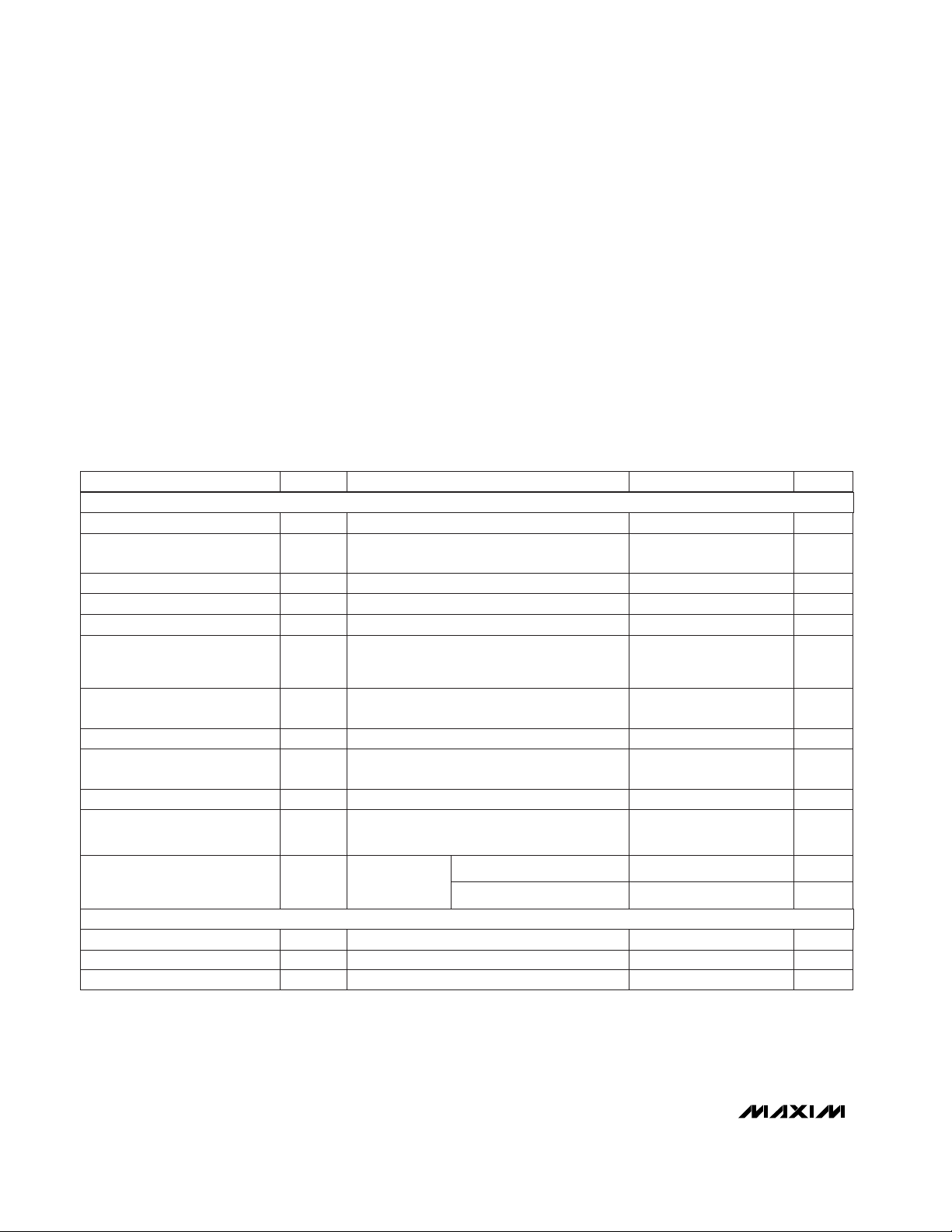
ABSOLUTE MAXIMUM RATINGS
ELECTRICAL CHARACTERISTICS
(V
OUT
= V
POUT
= V
LBP
= 3.6V, CLK/SEL = FB = LBN = LBO = ONA = ONB = TRACK = GND, REF = open (bypassed with 0.22µF),
LX = open, T
A
= 0°C to +85°C, unless otherwise noted. Typical values are at TA= +25°C.)
Stresses beyond those listed under “Absolute Maximum Ratings” may cause permanent damage to the device. These are stress ratings only, and functional
operation of the device at these or any other conditions beyond those indicated in the operational sections of the specifications is not implied. Exposure to
absolute maximum rating conditions for extended periods may affect device reliability.
ONA, ONB, FBLDO, OUT, POUT to GND...................-0.3V to 6V
PGND to GND.....................................................................±0.3V
POUT to OUT......................................................................±0.3V
LX to PGND ............................................-0.3V to (V
POUT
+ 0.3V)
CLK/SEL, REF, FB, TRACK, LDO,
LBN, LBP, LBO to GND.......................-0.3V to (V
OUT
+ 0.3V)
LDO Short Circuit.......................................................Continuous
Continuous Power Dissipation (T
A
= +70°C)
QSOP (derate 8.70mW/°C above +70°C)...................696mW
Operating Temperature Range ...........................-40°C to +85°C
Junction Temperature......................................................+150°C
Storage Temperature Range.............................-65°C to +160°C
Lead Temperature (soldering, 10sec).............................+300°C
CLK/SEL = OUT
-1µA < I
REF
< 50µA
(Note 1)
I
REF
= 0µA
CLK/SEL = GND, VFB= V
FBLDO
= 1.5V,
no load
ONA = GND, ONB = OUT, measure I
OUT
(Note 2)
V
POUT
= V
OUT
= 1.5V
VFB= 1.5V
MAX1705, 0A ≤ ILX≤ 0.5A;
MAX1706, 0A ≤ ILX≤ 0.25A;
CLK/SEL = OUT
TRACK = V
LDO
> 2.3V
CLK/SEL = OUT
CONDITIONS
mV4 15Reference Load Regulation
V1.238 1.250 1.262Reference Output Voltage
µA180 360
I
OUT
Supply Current in
Low-Noise Mode
V1.219 1.233 1.247FB Regulation Voltage
V0.7
Minimum Operating Battery
Voltage
µA100 190I
OUT
Supply Current in
Low-Power Mode
µA1 20I
OUT
Supply Current in Shutdown
V2.00 2.15 2.30
Start-Up to Normal Mode
Transition Voltage
kHz40 150 300f
LX
Frequency in Start-Up Mode
nA0.01 50FB Input Current
V2.5 5.5OUT Adjust Range
%0.65 1.25Load Regulation
V
V
LDO
V
LDO VLDO
+ 0.2 + 0.3 + 0.4
OUT Voltage in Track Mode
UNITSMIN TYP MAXSYMBOLPARAMETER
TA= +25°C, I
LOAD
< 1mA, Figure 2 V0.9 1.1Minimum Start-Up Voltage
2.5V < V
OUT
< 5.5V mV0.2 5Reference Supply Regulation
DC-DC CONVERTER
REFERENCE
VFB= V
FBLDO
= 1.5V, no load
FB = GND (LX switching) 2.1 mA
Page 3
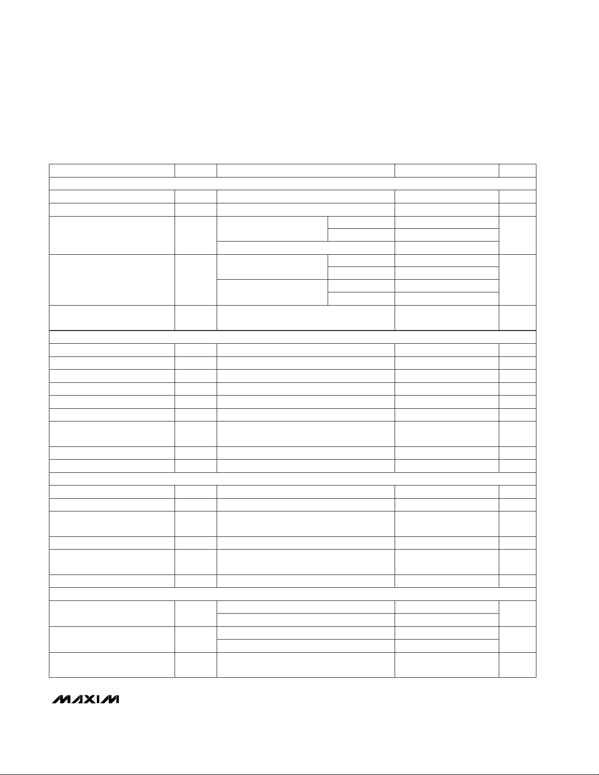
MAX1705/MAX1706
1- to 3-Cell, High-Current, Low-Noise,
Step-Up DC-DC Converters with Linear Regulator
_______________________________________________________________________________________
3
ELECTRICAL CHARACTERISTICS (continued)
(V
OUT
= V
POUT
= V
LBP
= 3.6V, CLK/SEL = FB = LBN = LBO = ONA = ONB = TRACK = GND, REF = open (bypassed with 0.22µF),
LX = open, T
A
= 0°C to +85°C, unless otherwise noted. Typical values are at TA= +25°C.)
f = 300kHz
V
OUT
= 5.5V, CLK/SEL, TRACK
V
LBO
= V
OUT
= 5V
I
SINK
= 1mA, V
OUT
= 2.5V, LBP = GND,
LBN = OUT
1.2V < V
OUT
< 5.5V, ONA, ONB (Note 3)
V
OUT
= 2.5V, CLK/SEL, TRACK
V
LBN
= VLBP = 1V
V
LBN
= 0.5V and 1.5V (at least one input must
be within this range)
Hysteresis approximately 10°C
LBP falling
1.2V < V
OUT
< 5.5V, ONA, ONB (Note 3)
LBP rising
CONDITIONS
µA1
Input Leakage Current
(CLK/SEL, ONA, ONB, TRACK)
0.8V
OUT
V
0.8V
OUT
Input High Level
0.2V
OUT
V
0.2V
OUT
Input Low Level
dB38AC Power-Supply Rejection
µA1LBO High Leakage
V0.4LBO Output Low Voltage
nA0.01 50LBN, LBP Input Current
V0.5 1.5
LBN, LBP Common-Mode
Input Range
°C155Thermal Shutdown
mV-5 5LBN, LBP Offset
mV16LBN, LBP Hysteresis
UNITSMIN TYP MAXSYMBOLPARAMETER
mA20 70 120
P-Channel SynchronousRectifier Turn-Off Current
VLX= 0V, V
ONB
= V
OUT
= 5.5V µA0.1 20POUT Leakage Current
CLK/SEL = GND
CLK/SEL = GND
250 435 550
CLK/SEL = OUT
mA
1000 1280 1550
I
LIM
N-Channel MOSFET
Current Limit
550 750 950
MAX1705
MAX1705
MAX1706
MAX1706 250 435 550
FBLDO = LDO, I
LOAD
= 1mA V1.238 1.250 1.262FBLDO Regulation Voltage
V
FBLDO
= 1.5V nA0.01 50FBLDO Input Current
FBLDO = GND mA220 300 500Short-Circuit Current Limit
V
FBLDO
= 1V, I
LDO
= 200mA
Ω
0.5 1.2Dropout Resistance
10µA < I
LDO
< 200mA, FBLDO = LDO %0.4 1.2Load Regulation
2.5V < V
OUT
< 5.5V, FBLDO = LDO,
I
LDO
= 1mA
%0.1 0.5Line Regulation
P-channel, ILX= 100mA 0.27 0.50
N-channel, ILX= 100mA
Ω
0.23 0.45
Switch On-Resistance
0.16 0.28
CLK/SEL = GND
CLK/SEL = OUT
VLX= 0V, V
ONB
= V
OUT
= 5.5V µA0.1 20LX Leakage Current
V1.25 5.0LDO Adjust Range
CONTROL INPUTS
LOW-BATTERY COMPARATOR
LINEAR REGULATOR
DC-DC SWITCHES
Page 4
MAX1705/MAX1706
1- to 3-Cell, High-Current, Low-Noise,
Step-Up DC-DC Converters with Linear Regulator
4 _______________________________________________________________________________________
ELECTRICAL CHARACTERISTICS (continued)
(V
OUT
= V
POUT
= V
LBP
= 3.6V, CLK/SEL = FB = LBN = LBO = ONA = ONB = TRACK = GND, REF = open (bypassed with 0.22µF),
LX = open, T
A
= 0°C to +85°C, unless otherwise noted. Typical values are at TA= +25°C.)
ELECTRICAL CHARACTERISTICS
(V
OUT
= V
POUT
= V
LBP
= 3.6V, CLK/SEL = FB = LBN = LBO = ONA = ONB = TRACK = GND, REF = open (bypassed with 0.22µF),
LX = open, T
A
= -40°C to +85°C, unless otherwise noted, Note 4.)
PARAMETER SYMBOL MIN TYP MAX UNITS
Minimum CLK/SEL Pulse
Internal Oscillator Frequency 260 300 340 kHz
200 ns
Maximum CLK/SEL
Rise/Fall Time
100 ns
CONDITIONS
CLK/SEL = OUT
Supply Current in
Low-Power Mode
I
OUT
190 µACLK/SEL = 0V, FB = FBLDO = 1.5V, no load
Supply Current in Shutdown I
OUT
20 µA
ONA = 0V, ONB = OUT, measure I
OUT
OUT Voltage in Track Mode
V
LDO
+ V
LDO
+
0.2 0.4
VTRACK = OUT, V
LDO
> 2.3V
250 570MAX1706
MAX1706
CLK/SEL = OUT
CLK/SEL = 0V
MAX1705
CLK/SEL = OUT
CLK/SEL = 0V
0.28
MAX1705
Switch On-Resistance
0.45
Ω
N-channel, ILX= 100mA
550 950
N-Channel MOSFET
Current Limit
I
LIM
1000 1700
mA
CLK/SEL = OUT
250 570
0.50
CLK/SEL = 0V
P-channel, ILX= 100mA
PARAMETER SYMBOL MIN TYP MAX
P-Channel SynchronousRectifier Turn-Off Current
UNITSCONDITIONS
20 120 mA
Start-Up to Normal Mode
Transition Voltage
2.0 2.3 V
FB Regulation Voltage 1.215 1.251 VCLK/SEL = OUT
Reference Output Voltage 1.235 1.265 VI
REF
= 0µA
Oscillator Maximum Duty Cycle 80 86 90 %
External Oscillator
Synchronization Range
200 400 kHz
Supply Current in
Low-Noise Mode
I
OUT
360 µA
CLK/SEL = OUT, V
FB
= V
FBLDO
= 1.5V,
no load
DC-DC CONVERTER
REFERENCE
DC-DC CONVERTER
Page 5
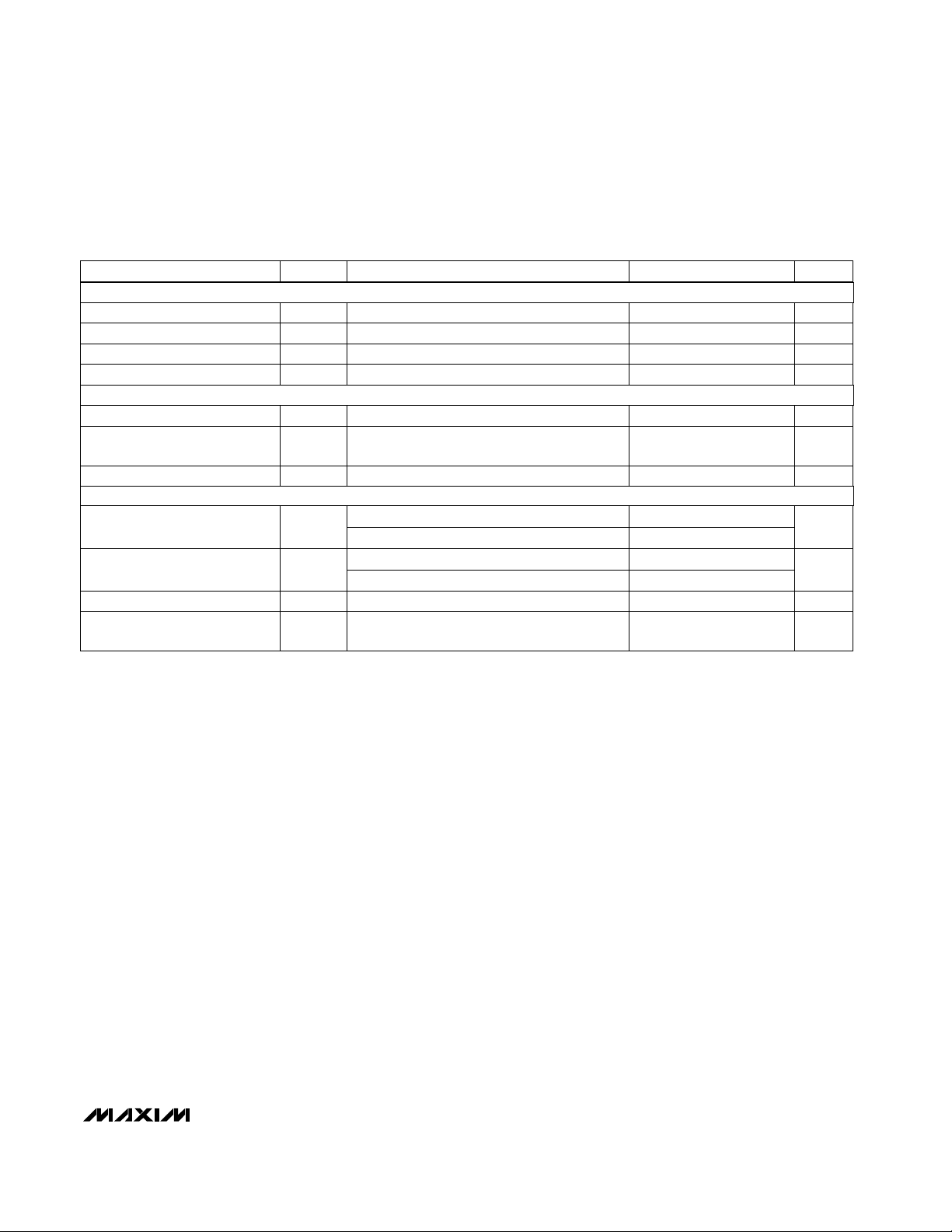
MAX1705/MAX1706
1- to 3-Cell, High-Current, Low-Noise,
Step-Up DC-DC Converters with Linear Regulator
_______________________________________________________________________________________ 5
ELECTRICAL CHARACTERISTICS (continued)
(V
OUT
= V
POUT
= V
LBP
= 3.6V, CLK/SEL = FB = LBN = LBO = ONA = ONB = TRACK = GND, REF = open (bypassed with 0.22µF),
LX = open, T
A
= -40°C to +85°C, unless otherwise noted, Note 4.)
PARAMETER SYMBOL MIN TYP MAX UNITS
LBN, LBP Common-Mode
Input Range
0.5 1.5 V
CONDITIONS
LBN = 0.5V and 1.5V (at least one input must
be within this range)
LBO High Leakage 1 µALBO = OUT = 5V
Input Low Level
0.15V
OUT
V
1.2V < V
OUT
< 5.5V, ONA, ONB (Note 2)
0.85V
OUT
1.2V < V
OUT
< 5.5V, ONA, ONB (Note 2)
Internal Oscillator Frequency 260 340 kHzCLK/SEL = OUT
External Oscillator
Synchronization Range
200 400 kHz
0.85V
OUT
V
OUT
= 5.5V, CLK/SEL, TRACK
Note 1: Once the output is in regulation, the MAX1705/MAX1706 operate down to a 0.7V input voltage.
Note 2: The device is in start-up mode when V
OUT
is below this value (see
Low-Voltage Start-Up Oscillator
section).
Note 3: ONA and ONB inputs have a hysteresis of approximately 0.15V
OUT
.
Note 4: Specifications to -40°C to are guaranteed by design, not production tested.
Input High Level
V
OUT
= 2.5V, CLK/SEL, TRACK 0.15V
OUT
V
LBN, LBP Offset -5 5 mVLBP falling
FBLDO Regulation Voltage 1.233 1.268 VFBLDO = LDO, I
LOAD
= 1mA
Short-Circuit Current Limit 220 600 mAFBLDO = LDO = GND
FBLDO Input Current 0.01 50 nAV
FBLDO
= 1.5V
Dropout Resistance 1.2 ΩV
FBLDO
= 1V, I
LDO
= 200mA
LINEAR REGULATOR
CONTROL INPUTS
LOW-BATTERY COMPARATOR
Page 6

MAX1705/MAX1706
1- to 3-Cell, High-Current, Low-Noise,
Step-Up DC-DC Converters with Linear Regulator
6 _______________________________________________________________________________________
__________________________________________Typical Operating Characteristics
(Circuit of Figure 2, TA= +25°C, unless otherwise noted.)
100
0
0.1 10 1001 1000
MAX1705
EFFICIENCY vs. OUTPUT CURRENT
(V
OUT
= 5V)
20
MAX1705/6 TOC02
OUTPUT CURRENT (mA)
EFFICIENCY (%)
40
60
80
90
10
30
50
70
L = 10µH
V
OUT
= 5V
A: V
IN
= 0.9V
C: V
IN
= 2.4V
E: V
IN
= 3.6V
1: PFM MODE
2: PWM MODE
A.1
A.2
C.1
C.2
B.2
B.1
100
0
0.1 10 1001 1000
MAX1705
EFFICIENCY vs. OUTPUT CURRENT
(V
OUT
= 3.3V)
20
MAX1705/6 TOC01
OUTPUT CURRENT (mA)
EFFICIENCY (%)
40
60
80
90
10
30
50
70
L = 10µH
V
OUT
= 3.3V
A: V
IN
= 0.9V
B: V
IN
= 2.7V
1: PFM MODE
2: PWM MODE
B.1
B.2
A.1
A.2
0
0
MAX1705
MAXIMUM OUTPUT CURRENT
vs. INPUT VOLTAGE
200
100
300
MAX1705/6 TOC03
INPUT VOLTAGE (V)
MAXIMUM OUTPUT CURRENT (mA)
3.5
700
600
900
800
400
500
1.0 2.5 4.5
1000
2.0 3.00.5 4.01.5
L = 10µH
PWM MODE
PFM MODE
V
OUT
= 3.3V
V
OUT
= 3.3V
V
OUT
= 5V
V
OUT
= 5V
100
0
0.1 10 1001 1000
MAX1706
EFFICIENCY vs. OUTPUT CURRENT
(V
OUT
= 3.3V)
20
MAX1705/6 TOC04
OUTPUT CURRENT (mA)
EFFICIENCY (%)
40
60
80
90
10
30
50
70
B.2
A.2
A.1
B.1
L = 22µH
V
OUT
= 3.3V
A: V
IN
= 0.9V
B: V
IN
= 2.7V
1: PFM MODE
2: PWM MODE
0.5
0.01
MAX1705
START-UP INPUT VOLTAGE
vs. OUTPUT CURRENT
0.9
0.7
1.1
MAX1705/6 TOC07
OUTPUT CURRENT (mA)
START-UP INPUT VOLTAGE (V)
100
1.7
1.5
2.1
1.9
1.3
0.1 10 1000
2.3
1
NO-LOAD START-UP:
1.0V AT -40°C
0.79 AT +25°C
0.64V AT +85°C
CONSTANT-CURRENT LOAD
V
OUT
= 3.3V
L = 10µH
D1 = MBR0520L
TA = -40°C
TA = +25°C
TA = +85°C
100
0
0.1 10 1001 1000
MAX1706
EFFICIENCY vs. OUTPUT CURRENT
(V
OUT
= 5V)
20
MAX1705/6 TOC05
OUTPUT CURRENT (mA)
EFFICIENCY (%)
40
60
80
90
10
30
50
70
A.1
A.2
C.2
B.2
C.1
B.1
L = 22µH
V
OUT
= 5V
A: V
IN
= 0.9V
B: V
IN
= 2.4V
C: V
IN
= 3.6V
1: PFM MODE
2: PWM MODE
0
0
MAX1706
MAXIMUM OUTPUT CURRENT
vs. INPUT VOLTAGE
200
100
300
MAX1705/6 TOC06
INPUT VOLTAGE (V)
MAXIMUM OUTPUT CURRENT (mA)
3.5
700
600
400
500
1.0 3 4.52.00.5 2.5 41.5
PWM MODE
L = 22µH
PFM MODE
V
OUT
= 5V
V
OUT
= 5V
V
OUT
= 3.3V
V
OUT
= 3.3V
0
0
NO-LOAD SUPPLY CURRENT
vs. INPUT VOLTAGE
2
1
3
MAX1705/6 TOC8
INPUT VOLTAGE (V)
NO-LOAD SUPPLY CURRENT (mA)
4.0
7
6
10
9
8
4
5
1.0 3.0 5.0
12
11
2.0 3.50.5 2.5 4.51.5
PFM MODE
PWM MODE
V
OUT
= 3.3V
L = 10µH
0
0
LINEAR-REGULATOR DROPOUT
VOLTAGE vs. LOAD CURRENT
20
40
MAX1705/6 TOC09
LOAD CURRENT (mA)
DROPOUT VOLTAGE (mV)
160
120
100
60
80
40 120 200
140
80
V
LDO
= 3.3V
V
LDO
= 2.5V
V
LDO
= 5V
Page 7

MAX1705/MAX1706
1- to 3-Cell, High-Current, Low-Noise,
Step-Up DC-DC Converters with Linear Regulator
_______________________________________________________________________________________ 7
____________________________Typical Operating Characteristics (continued)
(Circuit of Figure 2, TA= +25°C, unless otherwise noted.)
60
0
100 10k 100k 1M1k 10M
LINEAR-REGULATOR POWER-SUPPLY
REJECTION RATIO vs. FREQUENCY
10
20
MAX1705/6 TOC10
FREQUENCY (Hz)
PSRR (dB)
30
50
40
V
OUT
= 4V TO 5V
V
LDO
= 3.3V
I
LDO
= 200mA
C5 = 0.33µF
100
0
1 10050 200 250150 300
LINEAR-REGULATOR
REGION OF STABLE C6
ESR
vs. LOAD CURRENT
0.1
MAX1705/6 TOC11
LOAD CURRENT (mA)
C6 ESR (Ω)
1
10
STABLE REGION
C2 = 22pF (FEED FORWARD)
UNCOMPENSATED
C6 = 22µF
1k 10k 100k 1M 10M
MAX1705
NOISE SPECTRUM AT POUT
(V
OUT
= 4.5V, VIN = 1.2V, 200mA LOAD)
0V
MAX1705/6 TOC13
FREQUENCY (Hz)
NOISE (5mV
RMS/
div)
1k 10k 100k 1M 10M
MAX1705
LINEAR-REGULATOR OUTPUT NOISE SPECTRUM
(V
LDO
= 3.3V, V
OUT
= 4.5V, VIN = 1.2V, I
LDO
= 200mA)
0V
MAX1705/6 TOC14
FREQUENCY (Hz)
NOISE (50µV/div)
Page 8

MAX1705/MAX1706
1- to 3-Cell, High-Current, Low-Noise,
Step-Up DC-DC Converters with Linear Regulator
8 _______________________________________________________________________________________
____________________________Typical Operating Characteristics (continued)
(Circuit of Figure 2, TA= +25°C, unless otherwise noted.)
200µs/div
MAX1705
LINE-TRANSIENT RESPONSE
MAX1705/6 TOC15
I
OUT
= 0mA, V
OUT
= 3.3V
A = V
IN
, 1.5V TO 2.0V, 200mV/div
B = V
OUT,
10mV/div, 3.3V DC OFFSET
A
B
200µs/div
MAX1705
POWER-ON DELAY
(PWM MODE)
MAX1705/6 TOC17
VIN = 1.2V, LOAD = 1kΩ
A = ONA, 2V/div
B = V
LDO
, 2V/div
C = V
OUT
, 2V/div
D = INDUCTOR CURRENT, 500mA/div
A
C
D
3V
2.5V
3.3V
0mA
B
1µs/div
MAX1705
PWM SWITCHING WAVEFORMS
MAX1705/6 TOC18
VIN = 1.2V, V
OUT
= 4.5V, V
LDO
= 3.3V, I
LDO
= 200mA
A = INDUCTOR CURRENT, 500mA/div
B = LX VOLTAGE, 5V/div
C = V
OUT
RIPPLE, 50m/div AC COUPLED
D = V
LDO
RIPPLE, 5m/div AC COUPLED
C5 = 0.33µF
A
B
D
C
0V
1A
V
OUT
V
LDO
2µs/div
MAX1705
PFM SWITCHING WAVEFORMS
MAX1705/6 TOC19
VIN = 1.2V, V
OUT
= 4.5V, V
LDO
= 3.3V, I
LDO
= 40mA
A = INDUCTOR CURRENT, 500mA/div
B = LX VOLTAGE, 5V/div
C = V
OUT
RIPPLE, 50mV/div AC COUPLED
D = V
LDO
RIPPLE, 5mV/div AC COUPLED
C5 = 0.33µF
A
C
D
0mA
0V
V
OUT
V
LDO
B
1ms/div
MAX1705
LINEAR-REGULATOR
OUTPUT NOISE
MAX1705/6 TOC20
V
LDO
IS AC COUPLED, 1mv/div
I
LDO
= 200mA
C5 = 0.33µF
V
LDO
DC TO 500kHz
200µs/div
MAX1705
LOAD-TRANSIENT RESPONSE
MAX1705/6 TOC16
VIN = 1.2V, V
OUT
= 3.3V
A = V
OUT
, 50mV/div, 3.3V DC OFFSET
B = I
OUT
, 0mA TO 200mA, 200mA/div
A
B
Page 9

MAX1705/MAX1706
1- to 3-Cell, High-Current, Low-Noise,
Step-Up DC-DC Converters with Linear Regulator
_______________________________________________________________________________________ 9
______________________________________________________________Pin Description
Boost DC-DC Converter Power Output. POUT is the source of the P-channel synchronous-rectifier MOSFET
switch. Connect an external Schottky diode from LX to POUT. The output current available from POUT is
reduced by the current drawn from the LDO linear-regulator output.
POUT16
On Control Input. When ONA = high or ONB = low, the IC turns on. Connect ONA to OUT for normal
operation (Table 2).
ONA15
Off Control Input. When ONB = high and ONA = low, the IC is off. Connect ONB to GND for normal
operation (Table 2).
ONB
14
Inductor connection to the drains of the P-channel synchronous rectifier and N-channel switchLX13
Power Ground for the source of the N-channel power MOSFET switchPGND12
Low-Dropout Linear-Regulator Output. LDO sources up to 200mA. Bypass to GND with a 22µF capacitor.LDO9
Low-Battery Comparator Output. This open-drain, N-channel output is low when LBP < LBN.
Input hysteresis is 16mV.
LBO10
Switching-Mode Selection and External-Clock Synchronization Input:
• CLK/SEL = low: low-power, low-quiescent-current PFM mode.
• CLK/SEL = high: low-noise, high-power PWM mode. Switches at a constant frequency (300kHz). Full
output power is available.
• CLK/SEL = driven with an external clock: low-noise, high-power synchronized PWM mode.
Synchronizes to an external clock (from 200kHz to 400kHz).
Turning on the DC-DC converter with CLK/SEL = GND also serves as a soft-start function,
since peak inductor current is reduced.
CLK/SEL11
GroundGND5
Step-Up Converter Feedback Input, used during track mode. IC power and low-dropout linear-regulator
input. Bypass OUT to GND with a 0.1µF ceramic capacitor placed as close to the IC as possible.
OUT6
Step-Up DC-DC Converter Feedback Input. Connect FB to a resistor voltage divider between POUT and
GND to set the output voltage between 2.5V and 5.5V. FB regulates to 1.233V.
FB7
Low-Dropout Linear-Regulator Feedback Input. Connect FBLDO to a resistor voltage divider between LDO
to GND to set the output voltage from 1.25V to V
OUT
- 0.3V (5.0V max). FBLDO regulates to 1.250V.
FBLDO8
Track-Mode Control Input for DC-DC Converter. In track mode, the boost-converter output is sensed at
OUT and set 0.3V above LDO to improve efficiency. Set TRACK to OUT for track mode. Connect TRACK to
GND for normal operation.
TRACK4
1.250V Reference Output. Bypass REF with a 0.33µF capacitor to GND. REF can source up to 50µA.REF3
PIN
Low-Battery Comparator Inverting Input. Common-mode range is 0.5V to 1.5V.LBN2
Low-Battery Comparator Noninverting Input. Common-mode range is 0.5V to 1.5V.LBP1
FUNCTIONNAME
Page 10

MAX1705/MAX1706
1- to 3-Cell, High-Current, Low-Noise,
Step-Up DC-DC Converters with Linear Regulator
10 ______________________________________________________________________________________
_______________Detailed Description
The MAX1705/MAX1706 are designed to supply both
power and low-noise circuitry in portable RF and dataacquisition instruments. They combine a linear regulator, step-up switching regulator, N-channel power
MOSFET, P-channel synchronous rectifier, precision
reference, and low-battery comparator in a single 16pin QSOP package (Figure 1). The switching DC-DC
converter boosts a 1- or 2-cell input to an adjustable
output between 2.5V and 5.5V. The internal low-dropout
regulator provides linear post-regulation for noisesensitive circuitry, as well as outputs from 1.25V to
300mV below the switching-regulator output. The
MAX1705/MAX1706 start from a low, 1.1V input and
remain operational down to 0.7V.
These devices are optimized for use in cellular phones
and other applications requiring low noise during fullpower operation, as well as low quiescent current for
maximum battery life during standby and shutdown.
They feature constant-frequency (300kHz), low-noise
pulse-width-modulation (PWM) operation with 300mA or
730mA output capability from one or two cells, respectively, with 3.3V output. A low-quiescent-current standby pulse-frequency-modulation (PFM) mode offers an
output up to 60mA and 140µA, respectively, and
reduces quiescent power consumption to 500µW. In
shutdown mode, the quiescent current is further
reduced to just 1µA. Figure 2 shows the standard application circuit for the MAX1705 configured in highpower PWM mode.
Additional features include synchronous rectification for
high efficiency and improved battery life, and an
uncommitted comparator for low-battery detection. A
CLK/SEL input allows frequency synchronization to
reduce interference. Dual shutdown controls allow shutdown using a momentary pushbutton switch and microprocessor control.
LBP
FBLDO
OUT
2.15V
ONA
ON
ONB
REF
GND
CLK/SEL
FB
LDO
POUT
LX
PGND
LBO
LBN
REF
SHUTDOWN
LOGIC
THERMAL
SENSOR
MAX1705
MAX1706
ERROR
AMP
START-UP
OSCILLATOR
EN
Q
P
P
N
MOSFET DRIVER
WITH CURRENT
LIMITING
EN
300kHz
OSCILLATOR
EN
D
OSC
MODE
PFM/PWM
Q
Q
IFB
PFM/PWM
CONTROLLER
N
RDY
1.250V
REFERENCE
TRACK
IC PWR
IREF
V
OUT
- 300mV
V
LDO
ICS
OUT
Figure 1. Functional Diagram
Page 11

MAX1705/MAX1706
1- to 3-Cell, High-Current, Low-Noise,
Step-Up DC-DC Converters with Linear Regulator
______________________________________________________________________________________ 11
Step-Up Converter
The step-up switching DC-DC converter generates an
adjustable output to supply both power circuitry (such
as RF power amplifiers) and the internal low-dropout
linear regulator. During the first part of each cycle, the
internal N-channel MOSFET switch is turned on. This
allows current to ramp up in the inductor and store
energy in a magnetic field. During the second part of
each cycle, when the MOSFET is turned off, the voltage
across the inductor reverses and forces current
through the diode and synchronous rectifier to the output filter capacitor and load. As the energy stored in
the inductor is depleted, the current ramps down, and
the output diode and synchronous rectifier turn off.
Voltage across the load is regulated using either PWM
or PFM operation, depending on the CLK/SEL pin setting (Table 1).
Low-Noise, High-Power PWM Operation
When CLK/SEL is pulled high, the MAX1705/MAX1706
operate in a high-power, low-noise PWM mode. During
PWM operation, they switch at a constant frequency
(300kHz), and modulate the MOSFET switch pulse
width to control the power transferred per cycle and
regulate the voltage across the load. In PWM mode, the
devices can output up to 850mA. Switching harmonics
generated by fixed-frequency operation are consistent
and easily filtered.
During PWM operation, each of the internal clock’s rising edges sets a flip-flop, which turns on the N-channel
MOSFET switch (Figure 3). The switch is turned off
when the sum of the voltage-error and currentfeedback signals trips a multi-input comparator and
resets the flip-flop; the switch remains off for the rest of
the cycle. When a change occurs in the output voltage
error signal into the comparator, it shifts the level that
the inductor current is allowed to ramp to during each
cycle and modulates the MOSFET switch pulse width.
A second comparator enforces a 1.55A (max) inductor-
LX
POUT
OUT
BOOST OUTPUT 3.6V
FB
LDO OUTPUT 3.3V
INPUT 0.9V TO 3.6V
(TO PGND)
(TO PGND)
PGND
GND
LDO
FBLDO
LBO
LBN
REF
MAX1705
MAX1706
LBP
CLK/SEL
ONA
ONB
TRACK
R3
165k
R4
100k
R5
R6
R7
100k
C2*
D1
C7
22µF
C8
0.33µF
L1 10µH (22µH)
*OPTIONAL.
( ) ARE FOR MAX1706.
C4
220µF
(100µF)
C5*
0.33µF
C6
22µF
R1
191k
C3
0.1µF
C9
0.33µF
C1*
R2
100k
NOTE: HEAVY LINES INDICATE HIGH-CURRENT PATH.
Figure 2. Typical Operating Circuit (PWM Mode)
CLK/SEL MODE FEATURES
0 PFM Low supply current
1 PWM
Low noise,
high output current
External Clock
(200kHz to 400kHz)
Synchronized
PWM
Low noise,
high output current
Table 1. Selecting the Operating Mode
Page 12

MAX1705/MAX1706
1- to 3-Cell, High-Current, Low-Noise,
Step-Up DC-DC Converters with Linear Regulator
12 ______________________________________________________________________________________
current limit for the MAX1705, and 950mA (max) for the
MAX1706. During PWM operation, the circuit operates
with a continuous inductor current.
Synchronized PWM Operation
The MAX1705/MAX1706 can also be synchronized to a
200kHz to 400kHz frequency by applying an external
clock to CLK/SEL. This allows the user to set the harmonics, to avoid IF bands in wireless applications. The
synchronous rectifier is also active during synchronized
PWM operation.
Low-Power PFM Operation
Pulling CLK/SEL low places the MAX1705/MAX1706 in
low-power standby mode. During standby mode, PFM
operation regulates the output voltage by transferring a
fixed amount of energy during each cycle, and then
modulating the switching frequency to control the
power delivered to the output. The devices switch only
as needed to service the load, resulting in the highest
possible efficiency at light loads. Output current capability in PFM mode is 140mA (from 2.4V input to 3.3V
output). The output is regulated at 1.3% above the
PWM threshold.
During PFM operation, the error comparator detects
output voltage falling out of regulation and sets a
flip-flop, turning on the N-channel MOSFET switch
(Figure 4). When the inductor current ramps to the PFM
mode current limit (435mA) and stores a fixed amount
of energy, the current-sense comparator resets a flipflop. The flip-flop turns off the N-channel switch and
turns on the P-channel synchronous rectifier. A second
flip-flop, previously reset by the switch’s “on” signal,
inhibits the error comparator from initiating another
cycle until the energy stored in the inductor is dumped
into the output filter capacitor and the synchronous rectifier current ramps down to 70mA. This forces operation with a discontinuous inductor current.
Synchronous Rectifier
The MAX1705/MAX1706 feature an internal 270mΩ,
P-channel synchronous rectifier to enhance efficiency.
Synchronous rectification provides a 5% efficiency
improvement over similar nonsynchronous step-up
regulators. In PWM mode, the synchronous rectifier is
turned on during the second half of each cycle. In PFM
mode, an internal comparator turns on the synchronous
rectifier when the voltage at LX exceeds the step-up
converter output, and then turns it off when the inductor
current drops below 70mA.
Linear Regulator
The internal low-dropout linear regulator steps down the
output from the step-up converter and reduces switching
ripple. It is intended to power noise-sensitive analog circuitry, such as low-noise amplifiers and IF stages in cellular phones and other instruments, and can deliver up to
200mA. However, in practice, the maximum output current is further limited by the current available from the
boost converter and by the voltage differential between
OUT and LDO. Use a 22µF capacitor with a 1Ω or less
equivalent series resistance (ESR) at the output for stability (see the Linear Regulator Region of Stable C6 ESR
vs. Load Current graph in the
Typical Operating
Characteristics
). During power-up, the linear regulator
remains off until the step-up converter goes into regulation for the first time.
POUT
LX
PGND
P
N
S
Q
ICS
R
IFB*
IREF*
CURRENT
LIMIT LEVEL
OSC
*SEE FIGURE 1
Figure 3. Simplified PWM Controller Block Diagram
Figure 4. Controller Block Diagram in PFM Mode
LOGIC HIGH
D
Q
Q
R
IFB*
IREF*
CURRENT
LIMIT LEVEL
*SEE FIGURE 1
S
Q
R
POUT
P
LX
N
PGND
Page 13

MAX1705/MAX1706
1- to 3-Cell, High-Current, Low-Noise,
Step-Up DC-DC Converters with Linear Regulator
______________________________________________________________________________________ 13
The linear regulator in the MAX1705/MAX1706 features
a 0.5Ω, P-channel MOSFET pass transistor. This provides several advantages, including longer battery life,
over similar designs using a PNP pass transistor. The
P-channel MOSFET requires no base-drive current,
which reduces quiescent current considerably. PNPbased regulators tend to waste base-drive current in
dropout when the pass transistor saturates. The
MAX1705/MAX1706 eliminate this problem.
The linear-regulator error amplifier compares the output
feedback sensed at the FBLDO input against the internal 1.250V reference, and amplifies the difference
(Figure 1). The MOSFET driver reads the error signal
and applies the appropriate drive to the P-channel
pass transistor. If the feedback signal is lower than the
reference, the pass-transistor gate is pulled lower,
allowing more current to pass to the output, thereby
increasing the output voltage. If the feedback voltage is
too high, the pass-transistor gate is pulled up, allowing
less current to pass to the output. Additional blocks
include a current-limiting block and a thermal-overload
protection block.
Low-Voltage Start-Up Oscillator
The MAX1705/MAX1706 use a CMOS, low-voltage
start-up oscillator for a 1.1V guaranteed minimum startup input voltage at +25°C. On start-up, the low-voltage
oscillator switches the N-channel MOSFET until the output voltage reaches 2.15V. Above this level, the normal
step-up converter feedback and control circuitry take
over. Once the device is in regulation, it can operate
down to a 0.7V input, since internal power for the IC is
bootstrapped from the output using the OUT pin.
To reduce current loading during step-up, the linear
regulator is kept off until the start-up converter goes
into regulation. Minimum start-up voltage is influenced
by load and temperature (see the
Typical Operating
Characteristics
). To allow proper start-up, do not apply
a full load at POUT until after the device has exited
start-up mode and entered normal operation.
Shutdown
The MAX1705/MAX1706 feature a shutdown mode that
reduces quiescent current to less than 1µA, preserving
battery life when the system is not in use. During shutdown, the reference, the low-battery comparator, and
all feedback and control circuitry are off. The step-up
converter’s output drops to one Schottky diode drop
below the input, but the linear regulator output is
turned off.
Entry into shutdown mode is controlled by logic input
pins ONA and ONB (Table 2). Both inputs have trip
points near 0.5V
OUT
with 0.15V
OUT
hysteresis.
Tracking
Connecting TRACK to the step-up converter output
implements a tracking mode that sets the step-up
converter output to 300mV above the linear-regulator
output, improving efficiency. In track mode, feedback
for the step-up converter is derived from the OUT pin.
When TRACK is low, the step-up converter and linear
regulator are separately controlled by their respective
feedback inputs, FB and FBLDO. TRACK is a logic
input with a 0.5V
OUT
threshold, and should be hardwired or switched with a slew rate exceeding 1V/µs.
V
LDO
must be set above 2.3V for track mode to operate
properly.
On power-up with TRACK = OUT, the step-up convert-
er initially uses the FB input to regulate its output. After
the step-up converter goes into regulation for the first
time, the linear regulator turns on. When the linear regulator reaches 2.3V, track mode is enabled and the stepup converter is regulated to 300mV above the linearregulator output.
Low-Battery Comparator
The internal low-battery comparator has uncommitted
inputs and an open-drain output capable of sinking
1mA. To use it as a low-battery-detection comparator,
connect the LBN input to the reference, and connect
the LBP input to an external resistor divider between
the positive battery terminal and GND (Figure 2). The
resistor values are then as follows:
where V
IN,TH
is the desired input voltage trip point and
V
LBN
= V
REF
= 1.25V. Since the input bias current into
LBP is less than 50nA, R6 can be a large value (such
as 270kΩ or less) without sacrificing accuracy.
Connect the resistor voltage divider as close to the IC
as possible, within 0.2in. (5mm) of the LBP pin. The
inputs have a 0.5V to 1.5V common-mode input range,
and a 16mV input-referred hysteresis.
R R
V
V
INTH
LBN
5 6
,
=
- 1
ONA
ONB
MAX1705/MAX1706
0 0 On
0 1 Off
1 0 On
1 1 On
Table 2. On/Off Logic Control
Page 14

MAX1705/MAX1706
1- to 3-Cell, High-Current, Low-Noise,
Step-Up DC-DC Converters with Linear Regulator
14 ______________________________________________________________________________________
The low-battery comparator can also be used to monitor the output voltage, as shown in Figure 5.
To set the low-battery threshold to a voltage below the
1.25V reference, insert a resistor divider between REF
and LBN, and connect the battery to the LBP input
through a 10kΩ current-limiting resistor (Figure 6). The
equation for setting the resistors for the low-battery
threshold is then as follows:
Alternatively, the low-battery comparator can be used
to check the output voltage or to control the load directly on POUT during start-up (Figure 7). Use the following
equation to set the resistor values:
where V
OUT,TH
is the desired output voltage trip point
and V
LBP
is connected to the reference or 1.25V.
Reference
The MAX1705/MAX1706 have an internal 1.250V, 1%
bandgap reference. Connect a 0.33µF bypass capacitor to GND within 0.2in. (5mm) of the REF pin. REF can
source up to 50µA of external load current.
_________________ Design Procedure
Setting the Output Voltages
Set the step-up converter output voltage between 2.5V
and 5.5V by connecting a resistor voltage-divider to FB
from OUT to GND, as shown in Figure 8. The resistor
values are then as follows:
where VFB, the step-up regulator feedback setpoint, is
1.233V. Since the input bias current into FB is less than
50nA, R2 can have a large value (such as 270kΩ or
less) without sacrificing accuracy. Connect the resistor
voltage-divider as close to the IC as possible, within
0.2in. (5mm) of the FB pin.
Alternatively, set the step-up converter output to track
the linear regulator by 300mV. To accomplish this, set
TRACK to OUT.
R R
V
V
POUT
FB
1 2 =
- 1
R R
V
V
OUTTH
LBP
5 6
,
=
- 1
R R
V
V
REF
INTH
5 6
,
=
- 1
MAX1705
MAX1706
LBO
REF
LBN
POUT
GND
R5
R6
0.33µF
LDO
LBP
Figure 5. Using the Low-Battery Comparator to Sense
the Output Voltage
Figure 6. Detecting Battery Voltages Below 1.25V
Figure 7. Using the Low-Battery Comparator for Load Control
During Start-Up
POUT
MAX1705
MAX1706
LBO
R8
10k
BATTERY
VOLTAGE
P
C5
LBP
270k
REF
LBN
GND
STEP-UP OUTPUT
C3
0.1µF
C4
OUT
R5
R6
POUT
LBN
0.33µF
R5
0.33µF
LBO
LBP
REF
MAX1705
MAX1706
GND
R6
Page 15

MAX1705/MAX1706
1- to 3-Cell, High-Current, Low-Noise,
Step-Up DC-DC Converters with Linear Regulator
______________________________________________________________________________________ 15
To set the low-dropout linear-regulator output, use a
resistor voltage-divider connected to FBLDO from LDO
to GND. Set the output to a value at least 300mV less
than the step-up converter output using the following
formula:
where V
FBLDO
, the linear-regulator feedback trip point,
is 1.250V. Since the input bias current into FBLDO is
less than 50nA, R4 can be a large value (such as
270kΩ or less). Connect the resistor voltage-divider as
close to the IC as possible, within 0.2in. (5mm) of the
FBLDO pin.
Inductor Selection
The MAX1705/MAX1706’s high switching frequency
allows the use of a small surface-mount inductor. Use a
10µH inductor for the MAX1705 and a 22µH inductor
for the MAX1706. Make sure the saturation-current rating exceeds the N-channel switch current limit of 1.55A
for the MAX1705 and 950mA for the MAX1706. For high
efficiency, chose an inductor with a high-frequency
core material, such as ferrite, to reduce core losses. To
minimize radiated noise, use a torroid, pot core, or
shielded-bobbin inductor. See Table 3 for suggested
parts and Table 4 for a list of inductor suppliers.
Connect the inductor from the battery to the LX pin as
close to the IC as possible.
Attaching the Output Diode
Use a Schottky diode, such as a 1N5817, MBR0520L,
or equivalent. The Schottky diode carries current during
start-up, and in PFM mode after the synchronous rectifier turns off. Thus, the current rating only needs to be
500mA. Attach the diode between the LX and POUT
pins, as close to the IC as possible.
In high-temperature applications, some Schottky
diodes may be unsuitable due to high reverse-leakage
currents. Try substituting a Schottky diode with a higher
reverse voltage rating, or use an ultra-fast silicon rectifier with reverse recover times less than 60ns (such as a
MUR150 or EC11FS1). Do not use ordinary rectifier
diodes, since slow switching speeds and long reverse recovery times compromise efficiency and load
regulation.
Choose Input and Output
Filter Capacitors
Choose input and output filter capacitors that service
the input and output peak currents with acceptable
voltage ripple. Choose input capacitors with working
voltage ratings over the maximum input voltage, and
output capacitors with working voltage ratings higher
than the output.
A 100µF, 100mΩ, low-ESR tantalum capacitor is recommended at the MAX1706’s step-up output. For the
MAX1705, use two in parallel or a 220µF low-ESR tantalum capacitor. The input filter capacitor (C7) also
reduces peak currents drawn from the input source
and reduces input switching noise. The input voltage
source impedance determines the size required for the
input capacitor. When operating directly from one or
two NiCd cells placed close to the MAX1705/MAX1706,
use a 22µF, low-ESR input filter capacitor. When
operating from a power source placed farther away, or
R R
V
V
LDO
FBLDO
3 4 =
- 1
OUT
POUT
FB
FBLDO
LDO
GND
PGND
MAX1705
MAX1706
STEP-UP
OUTPUT
LINEAR-
REGULATOR
OUTPUT
R1
R2
R3
R4
C1*
C2*
* OPTIONAL COMPENSATION CAPACITORS
Figure 8. Feedback Connections for the MAX1705/MAX1706
PRODUCTION INDUCTORS CAPACITORS DIODES
Surface Mount
Sumida CDR63B, CD73, CDR73B, CD74B series
Coilcraft DO1608, DO3308, DT3316 series
Matsuo 267 series
Sprague 595D series
AVX TPS series
Motorola MBR0520L
Through Hole Sumida RCH654 series
Sanyo OS-CON series
Nichicon PL series
Motorola 1N5817
Table 3. Component Selection Guide
Page 16

MAX1705/MAX1706
1- to 3-Cell, High-Current, Low-Noise,
Step-Up DC-DC Converters with Linear Regulator
16 ______________________________________________________________________________________
from higher-impedance batteries, consider using one
or two 100µF, 100mΩ, low-ESR tantalum capacitors.
Low-ESR capacitors are recommended. Capacitor ESR
is a major contributor to output ripple—often more than
70%.
Ceramic, Sanyo OS-CON, and Panasonic SP/CB-series
capacitors offer the lowest ESR. Low-ESR tantalum
capacitors are second best and generally offer a good
trade-off between price and performance. Do not
exceed the ripple-current ratings of tantalum capacitors. Avoid aluminum-electrolytic capacitors, since their
ESR is too high.
Adding Bypass Capacitors
Several ceramic bypass capacitors are required for
proper operation of the MAX1705/MAX1706. Bypass
REF with a 0.33µF capacitor to GND. Connect a 0.1µF
ceramic capacitor from OUT to GND and a 0.33µF
ceramic capacitor from POUT to PGND. Place a 22µF,
low-ESR capacitor and an optional 0.33µF ceramic
capacitor from the linear-regulator output LDO to GND.
An optional 22pF ceramic capacitor can be added to
the linear-regulator feedback network to reduce noise
(C2, Figure 2). Place each of these as close to their
respective pins as possible, within 0.2in. (5mm) of the
DC-DC converter IC. High-value, low-voltage, surfacemount ceramic capacitors are now readily available in
small packages; see Table 4 for suggested suppliers.
Designing a PC Board
High switching frequencies and large peak currents
make PC board layout an important part of design.
Poor design can cause excessive EMI and groundbounce, both of which can cause instability or
regulation errors by corrupting voltage- and currentfeedback signals. It is highly recommended that the PC
board example of the MAX1705 evaluation kit (EV kit)
be followed.
Power components—such as the inductor, converter
IC, filter capacitors, and output diode—should be
placed as close together as possible, and their traces
should be kept short, direct, and wide. Place the LDO
output capacitor as close to the LDO pin as possible.
Make the connection between POUT and OUT very
short. Keep the extra copper on the board, and integrate it into ground as a pseudo-ground plane.
On multilayer boards, do not connect the ground pins
of the power components using vias through an internal
ground plane. Instead, place them close together and
route them in a star-ground configuration using component-side copper. Then connect the star ground to the
internal ground plane using vias.
Keep the voltage-feedback networks very close to the
MAX1705/MAX1706—within 0.2in. (5mm) of the FB and
FBLDO pins. Keep noisy traces, such as from the LX
pin, away from the reference and voltage-feedback networks, especially the LDO feedback, and separated
from them using grounded copper. Consult the
MAX1705/MAX1706 EV kit for a full PC board example.
__________ Applications Information
Use in a Typical
Wireless Phone Application
The MAX1705/MAX1706 are ideal for use in digital cordless and PCS phones. The power amplifier (PA) is connected directly to the step-up converter output for
maximum voltage swing (Figure 9). The internal linear
regulator is used for post-regulation to generate lownoise power for DSP, control, and RF circuitry. Typically,
RF phones spend most of their life in standby mode and
short periods in transmit/receive mode. During standby,
maximize battery life by setting CLK/SEL = GND and
TRACK = OUT; this places the IC in PFM and track
modes (for lowest quiescent power consumption). In
transmit/receive mode, set TRACK = GND and CLK/SEL
= OUT to increase the PA supply voltage and initiate
high-power, low-noise PWM operation. Table 5 lists the
typical available output current when operating with
one or more NiCd/NiMH cells or one Li-Ion cell.
Table 4. Component Suppliers
(847) 956-0702
81-3-3607-5144
USA: (847) 956-0666
Japan: 81-3-3607-5111
Sumida
(619) 661-1055
81-7-2070-1174
USA: (619) 661-6835
Japan: 81-7-2070-6306
Sanyo
(602) 994-6430USA: (602) 303-5454Motorola
(714) 960-6492USA: (714) 969-2491Matsuo
(847) 639-1469USA: (847) 639-6400Coilcraft
(803) 626-3123USA: (803) 946-0690
(800) 282-4975
AVX
FAXPHONESUPPLIER
Page 17

MAX1705/MAX1706
1- to 3-Cell, High-Current, Low-Noise,
Step-Up DC-DC Converters with Linear Regulator
______________________________________________________________________________________ 17
Implementing Soft-Start
To implement soft-start, set CLK/SEL low on power-up;
this forces PFM operation and reduces the peak switching current to 435mA. Once the circuit is in regulation,
CLK/SEL can be set high for full-power operation.
Adding a Manual Power Reset
A momentary pushbutton switch can be used to turn
the MAX1705/MAX1706 on and off (Figure 10). ONA is
pulled low and ONB is pulled high to turn the part off.
When the momentary switch is pressed, ONB is pulled
low and the regulator turns on. The switch must be
pressed long enough for the microcontroller (µC) to exit
reset (200ms) and drive ONA high. A small capacitor is
added to help debounce the switch. The µC issues a
logic high to ONA, which holds the part on regardless
of the switch state. To turn the regulator off, press the
switch again, allowing the µC to read the switch status
and pull ONA low. When the switch is released, ONB is
pulled high.
___________________Chip Information
TRANSISTOR COUNT: 1649
SUBSTRATE CONNECTED TO GND
MAX1705
2 NiCd/NiMH 2.4 3.3 730
2 NiCd/NiMH 2.4 5.0 500
3 NiCd/NiMH or 1 Li-Ion 3.6 5.0 850
MAX1706
450
350
550
Table 5. Typical Available Output Current
µC
V
DD
I/O
MAX1705
MAX1706
ONA
ONB
OUT
I/O
0.1µF
ON/OFF
270k
270k
Figure 10. Momentary Pushbutton On/Off Switch
MAX1705
MAX1706
PA
RF
LX POUT
GND LDO
CONTROL
INPUTS
µC
I/O
Figure 9. Typical Phone Application
1 NiCd/NiMH 1.2 3.3 300 200
NUMBER OF CELLS
INPUT VOLTAGE
(V)
STEP-UP OUTPUT VOLTAGE:
(PA POWER SUPPLY)
(V)
TOTAL OUTPUT CURRENT
(mA)
Page 18

MAX1705/MAX1706
1- to 3-Cell, High-Current, Low-Noise,
Step-Up DC-DC Converters with Linear Regulator
18 ______________________________________________________________________________________
4.0 ±0.1
0.30 ±0.05
0.8 ±0.05
0.30R MAX.
Bo
Ko
2.2 ±0.1
0.5 RADIUS
TYPICAL
A0
4.0 ±0.1
2.0 ±0.05
1.5 +0.1/-0.0 DIAMETER
1.75 ±0.1
1.0 ±0.1
A
8.0 ±0.3
3.5 ±0.05
1.0 MINIMUM
A
Ao = 3.1mm ±0.1
Bo = 2.7mm ±0.1
Ko = 1.2mm ±0.1
NOTE: DIMENSIONS ARE IN MM.
AND FOLLOW EIA481-1 STANDARD.
__________________________________________________Tape-and-Reel Information
Page 19

MAX1705/MAX1706
1- to 3-Cell, High-Current, Low-Noise,
Step-Up DC-DC Converters with Linear Regulator
______________________________________________________________________________________ 19
________________________________________________________Package Information
QSOP.EPS
Page 20

MAX1705/MAX1706
1- to 3-Cell, High-Current, Low-Noise,
Step-Up DC-DC Converters with Linear Regulator
20 ______________________________________________________________________________________
NOTES
 Loading...