

Page 1
19-6008; Rev 0; 9/11
MAX17047
ModelGauge m3 Fuel Gauge
General Description
The MAX17047 incorporates the Maxim ModelGauge™
m3 algorithm that combines the excellent short-term
accuracy and linearity of a coulomb counter with the
excellent long-term stability of a voltage-based fuel gauge,
along with temperature compensation to provide industryleading fuel-gauge accuracy. ModelGauge m3 cancels
offset accumulation error in the coulomb counter, while
providing better short-term accuracy than any purely
voltage-based fuel gauge. Additionally, the ModelGauge
m3 algorithm does not suffer from abrupt corrections that
normally occur in coulomb-counter algorithms, since tiny
continual corrections are distributed over time.
The device automatically compensates for aging, temperature, and discharge rate and provides accurate
state of charge (SOC) in mAh or % over a wide range of
operating conditions. The device provides two methods
for reporting the age of the battery: reduction in capacity
and cycle odometer.
The device provides precision measurements of current,
voltage, and temperature. Temperature of the battery
pack is measured using an external thermistor supported
by ratiometric measurements on an auxiliary input. A
2-wire (I2C) interface provides access to data and control
registers. The IC is available in a lead(Pb)-free, 3mm x
3mm, 10-pin TDFN package.
Applications
2.5G/3G/4G Wireless
Handsets
Smartphones/PDAs
Tablets and Handheld
Computers
Portable Game Players
e-Readers
Digital Still and Video
Cameras
Portable Medical Equipment
Features
S Accurate Battery-Capacity Estimation
Temperature, Age, and Rate Compensated
Does Not Require Empty, Full, or Idle States to
Maintain Accuracy
S Precision Measurement System
No Calibration Required
S ModelGauge m3 Algorithm
Long-Term Influence by Voltage Fuel Gauge
Cancels Coulomb-Counter Drift
Short-Term Influence by Coulomb Counter
Provides Excellent Linearity
Adapts to Cell Characteristics
S External Temperature-Measurement Network
Actively Switched Thermistor Resistive Divider
Reduces Current Consumption
S Low Quiescent Current
25µA Active, < 0.5µA Shutdown
S Alert Indicator for SOC, Voltage, Temperature, and
Battery Removal/Insertion Events
S AtRate Estimation of Remaining Capacity
S 2-Wire (I2C) Interface
S Tiny, Lead(Pb)-Free, 3mm x 3mm, 10-Pin TDFN
Package
Ordering Information appears at end of data sheet.
For related parts and recommended products to use with this part,
refer to: www.maxim-ic.com/MAX17047.related
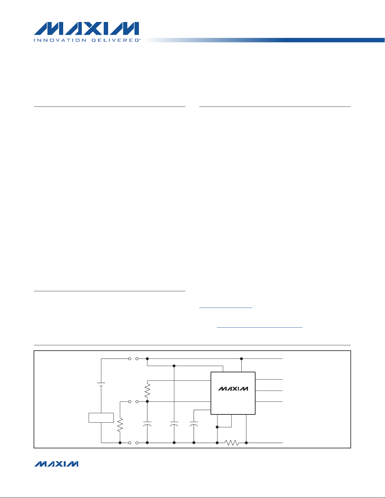
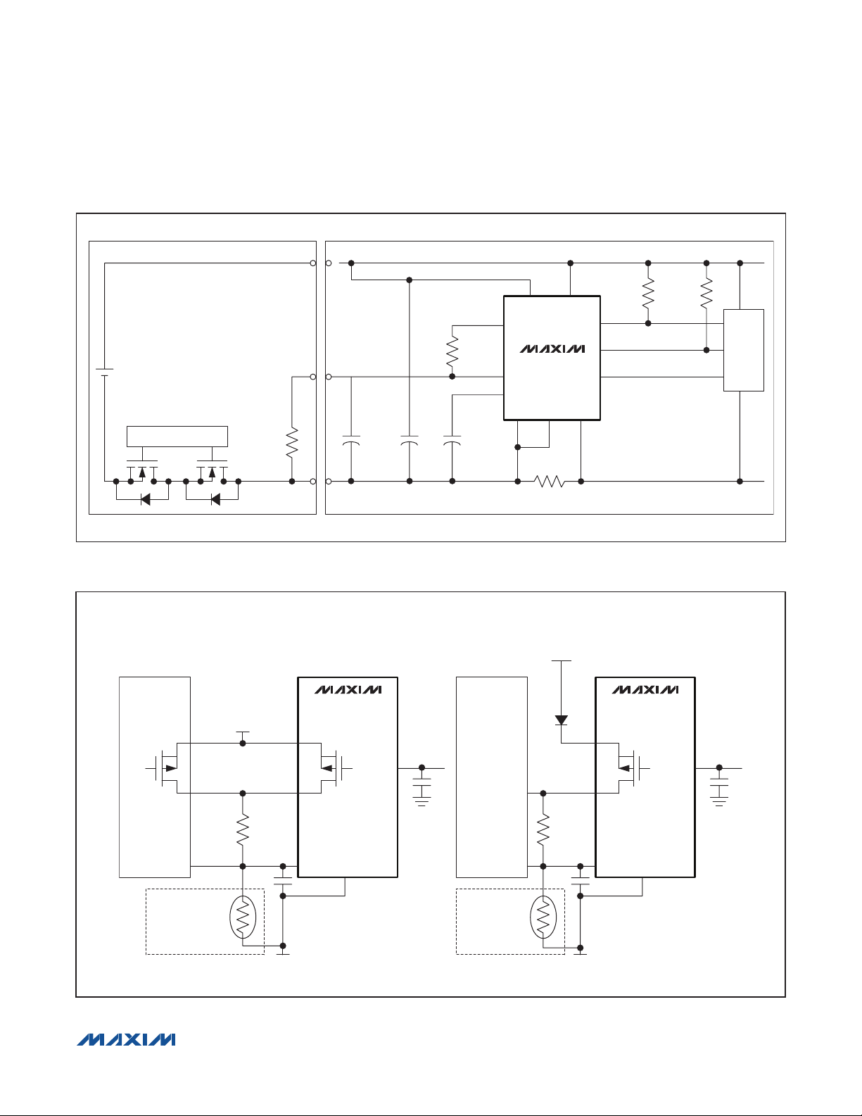
Simplified Operating Circuit
BATTERY PACK
PK+
OPTIONAL
10kI
T
PROTECTION
ModelGauge is a trademark of Maxim Integrated Products, Inc.
����������������������������������������������������������������� Maxim Integrated Products 1
OPTIONAL
10kI
NTC
THERMISTOR
PK-
OPTIONAL
10nF
V
BATTVTT
THRM
AIN SCL
REG
0.1µF0.1µF
MAX17047
CSP
10mI
RSNS
SYSTEM
ALRT
SDA
CSNEP
HOST
µP
For pricing, delivery, and ordering information, please contact Maxim Direct at 1-888-629-4642,
or visit Maxim’s website at www.maxim-ic.com.
Page 2

MAX17047
ModelGauge m3 Fuel Gauge
ABSOLUTE MAXIMUM RATINGS
V
, SDA, SCL, ALRT to CSP .............................-0.3V to +6V
BATT
REG to CSP ..........................................................-0.3V to +2.2V
VTT to CSP ............................................................... -0.3V to +6V
THRM, AIN to CSP .....................................-0.3V to (VTT + 0.3V)
CSN to CSP ................................................................-2V to +2V
Continuous Sink Current (VTT) ...........................................20mA
Stresses beyond those listed under “Absolute Maximum Ratings” may cause permanent damage to the device. These are stress ratings only, and functional operation of the device at these or any other conditions beyond those indicated in the operational sections of the specifications is not implied. Exposure to absolute
maximum rating conditions for extended periods may affect device reliability.
ELECTRICAL CHARACTERISTICS
(V
= 2.5V to 4.5V, TA = -20NC to +70NC, unless otherwise noted. Typical values are at TA = +25NC.) (Note 1)
BATT
PARAMETER SYMBOL CONDITIONS MIN TYP MAX UNITS
Supply Voltage V
Supply Current
REG Regulation Voltage V
Measurement Error, V
Measurement Resolution, V
V
Measurement Range V
BATT
BATT
BATT
BATT
I
DD0
I
DD1
V
GERR
V
REG
LSb
FS
Input Resistance CSN, AIN 15
Ratiometric Measurement
Accuracy, AIN
Ratiometric Measurement
Resolution, AIN
Current Register Resolution I
Current Full-Scale Magnitude I
Current Offset Error I
Current Gain Error I
Time-Base Accuracy t
T
GERR
T
LSb
OERR
GERR
ERR
LSb
FS
THRM Output Drive I
THRM Precharge Time t
SDA, SCL, ALRT
Input Logic High
PRE
V
IH
SDA, SCL, ALRT Input Logic Low V
SDA, ALRT Output Logic Low V
SDA, ALRT Pulldown Current I
OL
PD
ALRT Leakage 1
THRM Operating Range 2.5 V
(Note 2) 2.5 4.5 V
Shutdown mode, TA P +50NC
Active mode, average current 25 42
TA = +25NC
V
= 3.6V at TA = +25NC
DD
TA = 0NC to +50NC
TA = -20NC to +70NC
= 0.5mA V
OUT
0.5 V
IL
IOL = 4mA 0.4 V
Active mode, V
Continuous Sink Current (SCL, SDA, ALRT) ......................20mA
Operating Temperature Range .......................... -40NC to +85NC
Storage Temperature Range ............................ -55NC to +125NC
Lead Temperature (soldering 10s) .................................+300NC
Soldering Temperature (reflow) ......................................+260NC
0.5 2
1.5 1.9 V
-7.5 +7.5
-20 +20
0.625 mV
2.5 4.98 V
-0.5 +0.5 %
0.0244
1.5625
Q51.2
Q1.5 FV
-1 +1
-1 +1
-2.5 +2.5
-3.5 +3.5
- 0.1 V
TT
8.48 ms
1.5 V
SDA
= 0.4V, V
= 0.4V 0.05 0.2 0.4
ALRT
TT
FA
mV
MI
% Full
Scale
FV
mV
% of
Reading
%
FA
FA
V
����������������������������������������������������������������� Maxim Integrated Products 2
Page 3

MAX17047
ModelGauge m3 Fuel Gauge
ELECTRICAL CHARACTERISTICS (continued)
(V
= 2.5V to 4.5V, TA = -20NC to +70NC, unless otherwise noted. Typical values are at TA = +25NC.) (Note 1)
BATT
PARAMETER SYMBOL CONDITIONS MIN TYP MAX UNITS
Battery-Removal Detection
Threshold—V
AIN
Rising
Battery-Removal Detection
Threshold—V
AIN
Falling
Battery-Removal Detection
Comparator Delay
External AIN Capacitance
ELECTRICAL CHARACTERISTICS (2-WIRE INTERFACE)
(2.5V P V
SCL Clock Frequency f
Bus Free Time Between a STOP
and START Condition
Hold Time (Repeated)
START Condition
Low Period of SCL Clock t
High Period of SCL Clock t
Setup Time for a Repeated
START Condition
Data Hold Time t
Data Setup Time t
Rise Time of Both SDA and SCL
Signals
Fall Time of Both SDA and SCL
Signals
Setup Time for STOP Condition t
Spike Pulse Widths
Suppressed by Input Filter
Capacitive Load for Each Bus
Line
SCL, SDA Input Capacitance C
Note 1: Specifications are 100% tested at TA = +25°C. Limits over the operating range are guaranteed by design and
Note 2: All voltages are referenced to CSP.
Note 3: Timing must be fast enough to prevent the device from entering shutdown mode due to bus low for a period > 45s minimum.
Note 4: f
Note 5: The maximum t
Note 6: This device internally provides a hold time of at least 100ns for the SDA signal (referred to the minimum VIH of the SCL
Note 7: Filters on SDA and SCL suppress noise spikes at the input buffers and delay the sampling instant.
Note 8: CB—total capacitance of one bus line in pF.
P 4.5V, TA = -20NC to +70NC.) (Note 1)
BATT
PARAMETER SYMBOL CONDITIONS MIN TYP MAX UNITS
characterization.
must meet the minimum clock low time plus the rise/fall times.
SCL
HD:DAT
signal) to bridge the undefined region of the falling edge of SCL.
V
DETR
V
t
TOFF
DETF
V
- V
THRM
V
THRM
V
AIN
AIN
- V
AIN
step from 70% to 100% of V
ALRT falling; Alrtp = logic 0;
THRM
to
EnAIN = logic 1; FTHRM = logic 1
R
= 10kI NTC
THM
SCL
t
BUF
t
HD:STA
LOW
HIGH
t
SU:STA
HD:DAT
SU:DAT
t
R
t
SU:STO
t
SP
C
BIN
(Note 3) 0 400 kHz
(Note 4) 0.6
(Notes 5, 6) 0 0.9
(Note 5) 100 ns
F
(Note 7) 0 50 ns
(Note 8) 400 pF
B
has only to be met if the device does not stretch the low period (t
40 125 200 mV
70 150 230 mV
100
100 nF
1.3
1.3
0.6
0.6
20 +
0.1C
20 +
0.1C
B
B
300 ns
300 ns
0.6
60 pF
) of the SCL signal.
LOW
Fs
Fs
Fs
Fs
Fs
Fs
Fs
Fs
����������������������������������������������������������������� Maxim Integrated Products 3
Page 4
SDA
SCL
MAX17047
ModelGauge m3 Fuel Gauge
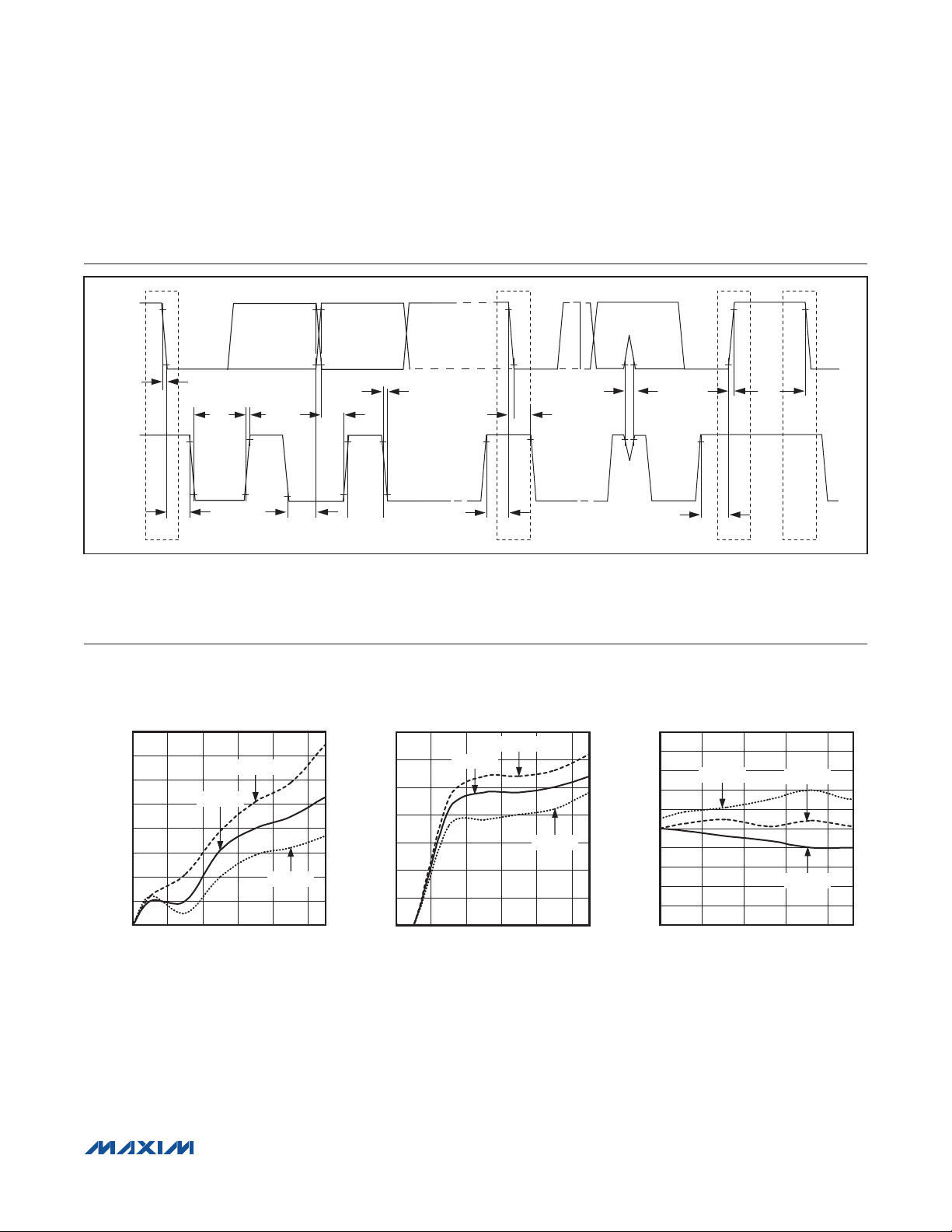
I2C Bus Timing Diagram
t
F
t
t
LOW
t
R
SU:DAT
t
F
t
HD:STA
t
SPtR
t
BUF
t
HD:STA
S Sr
Figure 1. I2C Bus Timing Diagram
(T
= +25°C, unless otherwise noted.)
A
SHUTDOWN CURRENT
vs. SUPPLY VOLTAGE
0.8
0.7
0.6
0.5
0.4
0.3
SHUTDOWN CURRENT (µA)
0.2
0.1
0
0
T
= +25°C
A
T
= +70°C
A
TA = -20°C
V
(V)
BATT
t
HD:DAT
t
SU:STA
t
SU:STO
P
S
Typical Operating Characteristics
ACTIVE CURRENT vs. SUPPLY VOLTAGE
35
30
MAX17047 toc01
25
20
15
ACTIVE CURRENT (µA)
10
5
541 2 3
0
0
= +25°C
T
A
T
= +70°C
A
MAX17047 toc02
TA = -20°C
54321
V
(V)
BATT
vs. TEMPERATURE AND SUPPLY VOLTAGE
10
8
6
4
2
0
-2
-4
VOLTAGE ADC ERROR (mV)
-6
-8
-10
2.2
VOLTAGE ADC ERROR
TA = -20°C
V
BATT
(V)
T
A
T
A
= +70°C
= +25°C
MAX17047 toc03
4.23.73.22.7
����������������������������������������������������������������� Maxim Integrated Products 4
Page 5
(T
= +25°C, unless otherwise noted.)
A
MAX17047
ModelGauge m3 Fuel Gauge
Typical Operating Characteristics (continued)
CURRENT ADC ERROR
vs. TEMPERATURE
15
10
5
0
-5
CURRENT ADC ERROR (mA)
TA = +25°C
-10
-15
-2 2
TA = -20°C
CURRENT FORCED (A)
RESPONSE TO TEMPERATURE TRANSIENT
AT CONSTANT-CURRENT LOAD
100
90
80
70
60
50
40
30
FUEL GAUGE CHANGES
SOC (%), TEMPERATURE (°C)
TRAJECTORY AFTER
20
TEMPERATURE CHANGE
10
0
TEMPERATURE
0 3
V
RISES WITH
CELL
TEMPERATURE DURING
CONSTANT LOAD
EMPTY VOLTAGE
21
TIME (Hr)
TA = +70°C
10-1
MAX17047 toc06
SOC
AV
SOC
REP
MAX17047 toc04
4.4
4.2
4.0
3.8
3.6
3.4
3.2
3.0
2.8
2.6
2.4
(V)
CELL
V
AUXILIARY INPUT ADC ERROR
vs. TEMPERATURE
1.00
0.80
0.60
0.40
0.20
0
-0.20
-0.40
-0.60
AUXILIARY INPUT ADC ERROR (%)
-0.80
-1.00
AIN RATIO TO VTT (%)
TA = -20°C
T
END-OF-CHARGE DETECTION
8000
FullCAP
7000
6000
V
5000
4000
3000
2000
1000
CAPACITY (mAh); CURRENT (mA)
-1000
-2000
CELL
0
0 8
VALID END-OF-CHARGE
DETECTION EVENT
RemCap
REP
TIME (Hr)
TA = +70°C
= +25°C
A
MAX17047 toc07
NEAR-FULL
FALSE CHARGE
TERMINATION
EVENTS
CURRENT
642
908060 7020 30 40 50100 100
MAX17047 toc05
4.7
4.5
4.3
4.1
3.9
3.7
3.5
3.3
3.1
2.9
2.7
(V)
CELL
V
����������������������������������������������������������������� Maxim Integrated Products 5
Page 6
(TA = +25°C, unless otherwise noted.)
MAX17047
ModelGauge m3 Fuel Gauge
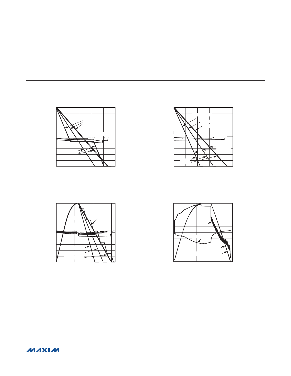
Typical Operating Characteristics (continued)
100
90
80
70
60
50
40
30
20
10
STATE OF CHARGE (%) OR TEMPERATURE (°C)
0
SOC
0 10
REFERENCE
SOC
ERROR
REP
TIME (Hr)
CHARGE AND DISCHARGE AT +20°C
100
90
COLD DISCHARGE (0°C)
80
70
60
50
40
STATE OF CHARGE (%)
30
20
10
0
0 15
SOC
REFERENCE
SOC
C/4 DISCHARGE
C/7 DISCHARGE
C/9 DISCHARGE
REP
C/2 DISCHARGE
ERROR
105
TIME (Hr)
MAX17047 toc08
8642
MAX17047 toc10
10
8
6
4
2
0
-2
-4
-6
-8
-10
10
8
6
4
2
0
-2
-4
-6
-8
-10
ERROR (%)
ERROR (%)
100
90
80
70
60
50
40
STATE OF CHARGE (%)
30
20
10
0
0 10
SOC
C/4 DISCHARGE
C/4 DISCHARGE
C/4 DISCHARGE
ERROR
REP
TIME (Hr)
CHARGE AND DISCHARGE IN
ACTUAL SYSTEM
100
90
80
DISCHARGE AT +40°C
70
60
50
40
30
20
10
STATE OF CHARGE (%) OR TEMPERATURE (°C)
0
0
V
CELL
TEMPERATURE
SOC
REFERENCE SOC
TIME (Hr)
REP
(%)
MAX17047 toc09
REFERENCE
SOC
8642
MAX17047 toc11
(%)
105
10
8
6
4
2
0
-2
-4
-6
-8
-10
4.2
4.1
4.0
3.9
3.8
3.7
3.6
3.5
3.4
3.3
3.2
ERROR (%)
(V)
CELL
V
����������������������������������������������������������������� Maxim Integrated Products 6
Page 7
TOP VIEW
MAX17047
ModelGauge m3 Fuel Gauge
Pin Configuration
V
SCL
SDA
+
1
TT
2 9
3
4
5 6
MAX17047
TDFN
V
10
BATT
THRMAIN
ALRT
8
REG
7
EP
CSPCSN
PIN NAME FUNCTION
1 V
2 AIN
Supply Input for Thermistor Bias Switch. Connect to supply for ratiometric AIN pin-voltage measurements.
TT
In most applications, connect VTT to V
BATT
.
Auxiliary Voltage Input. Auxiliary voltage input from external thermal-measurement network. AIN also
provides battery insertion/removal detection. Connect to V
, if not used.
BATT
3 SCL Serial Clock Input. 2-wire clock line. Input only.
4 SDA Serial Data Input/Out. 2-wire data line. Open-drain output driver.
5 CSN Sense Resistor Connection. System ground connection and sense resistor input.
6 CSP Chip Ground and Sense Resistor Input
7 REG
Voltage Regulator Bypass. Connect a 0.1FF capacitor from REG to CSP.
Alert Indication. An open-drain n-channel output used to indicate specified condition thresholds have been
8 ALRT
met. A 200kI pullup resistor to power rail is required for use as an output. Alternatively, ALRT can operate
as a shutdown input with the output function disabled.
9 THRM
10 V
BATT
Thermistor Bias Connection. Supply for thermistor resistor-divider. Connect to the high side of the
thermistor/resistor-divider. THRM connects internally to VTT during temperature measurement.
Power-Supply and Battery Voltage-Sense Input. Kelvin connect to positive terminal of battery pack. Bypass
with a 0.1FF capacitor to CSP.
— EP Exposed Pad. Connect to CSP.
Pin Description
����������������������������������������������������������������� Maxim Integrated Products 7
Page 8
0.1µF
PK-
PK+
0.1µF
10nF
PK+
PK-
PK-
V
BATT
REG
V
TT
THRM
V
THRM
- V
DETR/VDETF
AIN
MAX17047
ModelGauge m3 Fuel Gauge
Block Diagram
IN
2V LDO
OUT
P
PK- SYSTEM GROUND
32kHz OSCILLATOR
OCV CALCULATION
MAX17047
BATTERY
REMOVAL
DETECT
CSP CSN
10mI
RSNS
V
BATT
MUX
REF ADC
12-BIT ADC
ModelGauge m3
ALGORITHM
REF
2
I
C
INTERFACE
ALRT
CSP
SDA
SCL
Detailed Description
The MAX17047 incorporates the Maxim ModelGauge m3
algorithm that combines the excellent short-term accuracy and linearity of a coulomb counter with the excellent
long-term stability of a voltage-based fuel gauge, along
with temperature compensation to provide industryleading fuel-gauge accuracy. ModelGauge m3 cancels
offset accumulation error in the coulomb counter, while
providing better short-term accuracy than any purely
voltage-based fuel gauge. Additionally, the ModelGauge
m3 algorithm does not suffer from abrupt corrections that
normally occur in coulomb-counter algorithms, since tiny
continual corrections are distributed over time.
The device automatically compensates for aging, temperature, and discharge rate and provides accurate SOC
in mAh or % over a wide range of operating conditions.
The device provides two methods for reporting the age
of the battery: reduction in capacity and cycle odometer.
The device provides precision measurements of current,
voltage, and temperature. Temperature of the battery
pack is measured using an external thermistor supported
����������������������������������������������������������������� Maxim Integrated Products 8
by ratiometric measurements on an auxiliary input. A
2-wire (I2C) interface provides access to data and control
registers. The device is available in a 3mm x 3mm, 10-pin
TDFN package.
ModelGauge m3 Algorithm
The ModelGauge m3 algorithm combines a high-accuracy coulomb counter with a voltage fuel gauge (VFG) as
represented in Figure 2.
Classical coulomb-counter-based fuel gauges have
excellent linearity and short-term performance. However,
they suffer from drift due to the accumulation of the offset
error in the current-sense measurement. Although the
offset error is often very small, it cannot be eliminated,
causes the reported capacity error to increase over
time, and requires periodic corrections. Corrections are
usually performed at full or empty. Some other systems
also use the relaxed battery voltage to perform corrections. These systems determine the SOC based on the
battery voltage after a long time of no current flow. Both
have the same limitation: if the correction condition is not
observed over time in the actual application, the error in
Page 9
RELAXED
CELL
DETECTION
VOLTAGE
OCV TEMPERATURE-
COMPENSATION LEARN
CAPACITY LEARN
mAh PER %
ModelGauge m3 Fuel Gauge
VOLTAGE FUEL GUAGE
OCV CALCULATION
OCV OUTPUT
EMPTY
DETECTION
OCV TABLE LOOKUP
% REMAINING OUTPUT
MIXING ALGORITHM
mAh OUTPUT
RemCap
MIX
SOC
MIX
MAX17047
COULOMB COUNTER
mAh OUTPUT
CURRENT
TIME
CURRENT
TEMPERATURE
APPLICATION
EMPTY
COMPENSATION
END-OF-CHARGE
DETECTION
Figure 2. ModelGauge m3 Overview
the system is boundless. The performance of classic
coulomb counters is dominated by the accuracy of such
corrections.
Classical voltage-measurement-based SOC estimation
has poor accuracy due to inadequate cell modeling, but
does not accumulate offset error over time.
The device includes an advanced VFG, which estimates
open-circuit voltage (OCV), even during current flow, and
simulates the nonlinear internal dynamics of a lithium-ion
(Li+) battery to determine the SOC with improved accuracy. The model considers the time effects of a battery
caused by the chemical reactions and impedance in the
battery to determine SOC based on table lookup. This
SOC estimation does not accumulate offset error over
time.
The ModelGauge m3 algorithm combines a high-accuracy coulomb counter with a VFG. The complementary
APPLICATION
OUTPUTS:
SOC
REP
RemCap
REP
SOC
AV
RemCap
AV
TTE
FullCAP
CELL CHEMISTRY
OUTPUTS:
OCV
CYCLES
R
CELL
FullCAPNom
AGE
combined result eliminates the weaknesses of both the
coulomb counter and the VFG, while providing the
strengths of both. A mixing algorithm combines the VFG
capacity with the coulomb counter and weighs each
result so that both are used optimally to determine the
battery state. In this way, the VFG capacity result is used
to continuously make small adjustments to the battery
state, canceling the coulomb-counter drift.
The ModelGauge m3 algorithm uses this battery state
information and accounts for temperature, battery current, age, and application parameters to determine the
remaining capacity available to the system.
The ModelGauge m3 algorithm continually adapts to the
cell and application through independent learning routines. As the cell ages, its change in capacity is monitored
and updated and the VFG dynamics adapt based on cellvoltage behavior in the application.
����������������������������������������������������������������� Maxim Integrated Products 9
Page 10
MAX17047
ModelGauge m3 Fuel Gauge
OCV Estimation and Coulomb-Count Mixing
The core of the ModelGauge m3 algorithm is a mixing
algorithm that combines the OCV state estimation with
the coulomb counter. After power-on reset of the IC,
coulomb-count accuracy is unknown. The OCV state
estimation is weighted heavily compared to the coulombcount output. As the cell progresses through cycles in
the application, coulomb-counter accuracy improves
and the mixing algorithm alters the weighting so that the
coulomb-counter result is dominant. From this point forward, the IC switches to servo mixing. Servo mixing provides a fixed magnitude error correction to the coulomb
count, up or down, based on the direction of error from
the OCV estimation. This allows differences between
the coulomb count and OCV estimation to be corrected
quickly. See Figure 3.
100%
COULOMB-COUNT INFLUENCE SERVO MIXING
MIXING RATIO
OCV AND COULOMB-COUNT
OCV
INFLUENCE
0%
CELL CYCLES
Figure 3. ModelGauge m3 OCV and Coulomb-Count Mixing
1.501.000.500
2.00
The resulting output from the mixing algorithm does
not suffer drift from current measurement offset error
and is more stable than a stand-alone OCV estimation
algorithm; see Figure 4. Initial accuracy depends on the
relaxation state of the cell. The highest initial accuracy is
achieved with a fully relaxed cell.
Fuel-Gauge Empty Compensation
As the temperature and discharge rate of an application changes, the amount of charge available to the
applica tion also changes. The ModelGauge m3 algorithm dis tinguishes between remaining capacity of the
cell (RemCap
) and remaining capacity of the appli-
MIX
cation (RemCapAV) and reports both results to the user.
Fuel-Gauge Learning
The device periodically makes internal adjustments
to cell characterization and application information to
remove initial error and maintain accuracy as the cell
ages. These adjustments always occur as small undercorrections to prevent instability of the system and
prevent any noticeable jumps in the fuel-gauge outputs.
Learning occurs automatically without any input from the
host. To maintain learned accuracy through power loss,
the host must periodically save learned information and
then restore after power is returned. See the Power-Up
and Power-On Reset section for details:
• Application Capacity (FullCAP). This is the total
capacity available to the application at full. Through the
user-defined registers, ICHGTerm and FullSOCThr,
the device detects end-of-charge conditions as the
cell is cycled. These points allow the device to learn
the capacity of the cell based on the charge termination experienced during operation.
TYPICAL OCV ESTIMATION
ERROR AS CELL IS CYCLED
STATE-OF-CHARGE ERROR
TIME
Figure 4. ModelGauge m3 Algorithm Mixing Conceptual Illustration
���������������������������������������������������������������� Maxim Integrated Products 10
MAXIMUM COULOMB-COUNTER ERROR
(SHADED AREA)
ModelGauge m3
OCV + COULOMB-COUNT MIXING
MAXIMUM ERROR RANGE
Page 11

MAX17047
ModelGauge m3 Fuel Gauge
• Cell Capacity (FullCapNom). This is the total cell
capacity at full, according to the VFG. This includes
some capacity that is not available to the application
at high loads and/or low temperature. The device
periodically compares percent change based on OCV
measurement vs. coulomb-count change as the cell
charges and discharges. This information allows the
device to maintain an accurate estimation of the cell’s
capacity in mAh as the cell ages.
• Voltage Fuel-Gauge Adaptation. The device
observes the battery’s relaxation response and
adjusts the dynamics of the VFG. This adaptation
adjusts the RCOMP0 register during qualified cell
relaxation events.
• Empty Compensation. The device updates inter-
nal data whenever cell empty is detected (V
V�empty) to account for cell age or other cell deviations from the characterization information.
CELL
<
Determining Fuel-Gauge Accuracy
To determine the true accuracy of a fuel gauge, as experienced by end users, the battery should be exercised
in a dynamic manner. The end-user accuracy cannot be
understood with only simple cycles.
To challenge a correction-based fuel gauge, such as
coulomb counters, test the battery with partial loading
sessions. For example, a typical user may operate the
device for 10min and then stop using for an hour or more.
A robust test method includes these kinds of sessions
many times at various loads, temperatures, and duration.
Refer to Application Note 4799: Cell Characterization
Procedure for a ModelGauge m3 Fuel Gauge.
Initial Accuracy
The device uses the first voltage reading after power-up
or after cell insertion to determine the starting output of
the fuel gauge. It is assumed that the cell is fully relaxed
prior to this reading; however, this is not always the
case. If the cell was recently charged or discharged, the
voltage measured by the device may not represent the
true state of charge of the cell, resulting in initial error in
the fuel gauge outputs. In most cases, this error is minor
and is quickly removed by the fuel gauge algorithm during normal operation.
Typical Operating Circuit
The device is designed to mount outside the cell pack
that it monitors. Voltage of the battery pack is measured
directly at the pack terminals by the V
connections. Current is measured by an external sense
resistor placed between the CSP and CSN pins. An
external resistor-divider network allows the device to
measure temperature of the cell pack by monitoring the
AIN pin. The THRM pin provides a strong pullup for the
resistor-divider that is internally disabled when temperature is not being measured.
Communication to the host occurs over a standard I2C
interface. SCL is an input from the host, and SDA is an
open-drain I/O pin that requires an external pullup. The
ALRT pin is an output that can be used as an external
interrupt to the host processor if certain application conditions are detected. ALRT can also function as an input,
allowing the host to shut down the device. This pin is
also open drain and requires an external pullup resistor.
Figure 5 is the typical operating circuit.
The device can share the cell thermistor circuit with the
system charger. In this circuit, there is a single thermistor inside the cell pack and a single bias resistor external to the cell pack. The device shares the same external bias as the charger circuit and measurement point
on the thermistor. In this configuration, each device
can measure temperature individually or simultaneously
without interference. Alternatively, if the bias voltage in
the charger circuit is not available to the device, a separate bias voltage on the VTT pin can be used. For proper
operation, the separate bias voltage must be larger than
the minimum operating voltage of the device, but no
larger than one diode drop above the charger circuit
bias voltage. See Figure 6.
BATT
and CSP
���������������������������������������������������������������� Maxim Integrated Products 11
Page 12
MAX17047
ModelGauge m3 Fuel Gauge
BATTERY PACK
THERMISTOR
MEASUREMENT OPTIONAL
OPTIONAL
PROTECTION IC
THERMISTOR
Figure 5. Typical Operating Circuit
10kI
NTC
PK+
T
PK-
OPTIONAL
10nF
V
BATTVTT
THRM
OPTIONAL
10kI
REG
0.1µF0.1µF
MAX17047
AIN SCL
CSP
10mI
RSNS
BIAS
V
< V
2.8V < V
BIAS
INTERNAL
SYSTEM
OPTIONAL
ALRT
SDA
CSNEP
+ 0.6V
200kI
OPTIONAL
5kI
HOST
µP
CHARGER WITH
V
+ THRM
TT
AVAILABLE
THERMISTOR
CELL PACK
V
BIAS
VOLTAGE BASED
P P
ON EXISTING
CHARGER REQUIREMENTS
INSIDE
V
THRM
AIN
MAX17047 + CHARGER
PK- PK-
MAX17047
TT
CSP
WITH EXTERNAL BIAS
V
SYSTEM
V
BATT
CHARGER WITH
INTERNAL
OFF DURING
DISCHARGE
THERMISTOR
CELL PACK
Figure 6. Operating Circuits that Share Pack Thermistor with System Charger
���������������������������������������������������������������� Maxim Integrated Products 12
BIAS
V
INTERNAL
ON DURING
CHARGE
INSIDE
MAX17047
V
TT
P
THRM
AIN
CSP
MAX17047 + CHARGER
WITH INTERNAL BIAS
V
SYSTEM
V
BATT
Page 13
MAX17047
ModelGauge m3 Fuel Gauge
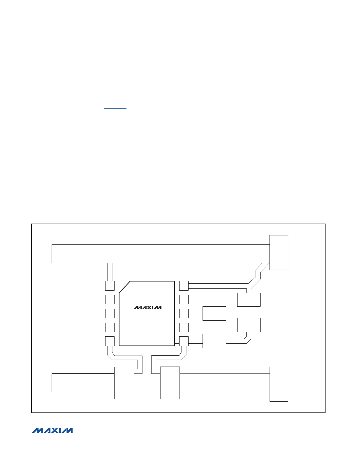
Recommended Layout
Proper circuit layout (see Figure 7) is essential for
measurement accuracy when using the MAX17047
ModelGauge m3 IC. The recommended layout guidelines are as follows:
1) Mount R
device shares both voltage and current measurements on the CSP pin. Therefore, it is important to limit
the amount of trace resistance between the currentsensing resistor and PACK-.
2) V
BATT
PACK+. The device shares the V
voltage measurement and IC power. Limiting the
voltage loss through this trace is important to voltagemeasurement accuracy. PCB resistance that cannot
be removed can be compensated for during characterization of the application cell.
POSITIVE POWER BUS
as close as possible to PACK-. The
SNS
trace should make a Kelvin connection to
pin for both
BATT
3) CSN and CSP traces should make Kelvin connections
to R
. The device measures current differentially
SNS
through the CSN and CSP pins. Any shared highcurrent paths on these traces will affect currentmeasurement gain accuracy. PCB resistance that
cannot be removed can be compensated for during
characterization of the application cell.
4) V
capacitor trace loop area should be minimized.
BATT
The device shares the V
pin for both voltage mea-
BATT
surement and IC power. Limiting noise at the V
BATT
pin is important to current-measurement accuracy.
5) REG capacitor trace loop area should be minimized.
The helps filter any noise from the internal regulated
supply.
6) There are no limitations on any other IC connection.
Connections to THRM, ALRT, SDA, SCL, VTT, and
AIN, as well as any external components mounted to
these pins, have no special layout requirements.
PACK +
CONTACT
NEGATIVE POWER BUS
Figure 7. Proper Board Layout
���������������������������������������������������������������� Maxim Integrated Products 13
V
AIN
SCL
SDA
CSN
V
BATT
TT
THRM
MAX17047
EP
R
SNS
REG
ALRT
CSP
C
REG
C
VBATT
PACK CONTACT
Page 14
MAX17047
ModelGauge m3 Fuel Gauge
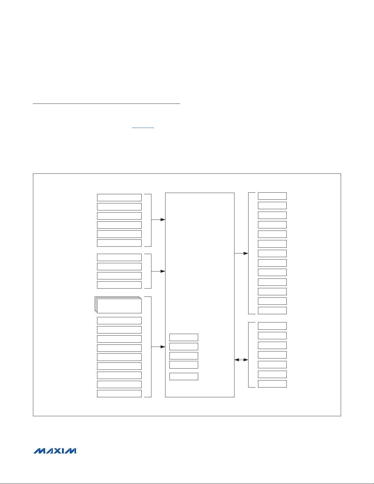
ModelGauge m3 Registers
To calculate accurate results, ModelGauge m3 requires
information about the cell, the application, and real-time
information measured by the device. Figure 8 shows all
inputs and outputs to the algorithm grouped by category.
Analog input registers are the real-time measurements
of voltage, temperature, and current performed by the
device. Application-specific registers are programmed
by the customer to reflect the operation of the applica-
V
CELL
CURRENT
ANALOG
INPUTS
APPLICATION
SPECIFIC
CELL
CHARACTERIZATION
INFORMATION
TEMPERATURE
AverageV
CELL
AverageCurrent
AverageTemperature
DesignCap
ICHGTerm
FullSOCThr
V_empty
CHARACTERIZATION
TABLE
QResidual Table
FCTC
RCOMP0
TempCo
TempNom
TempLim
V_empty
FullCapNom
Iavg_empty
LearnCFG
FilterCFG
RelaxCFG
MiscCFG
tion. The Cell Characterization Information registers
hold characterization data that models the behavior of
the cell over the operating range of the application. The
Algorithm Configuration registers allow the host to adjust
performance of the device for their application. The Save
and Restore registers allow an application to maintain
accuracy of the algorithm after the device has been
power cycled. The following sections describe each
register in detail.
SOC
MIX
RemCap
MIX
SOC
REP
RemCap
REP
SOC
AV
RemCap
AV
ModelGauge
ALGORITHM
OUTPUTS
SAVE AND
RESTORE
INFORMATION
ModelGauge ALGORITHM
ALGORITHM
CONFIGURATION
AtRate
TTE
AGE
CYCLES
OCV
FullCAP
FullCapNom
FSTAT
FullCAP
CYCLES
QResidual Table
RCOMP0
TempCo
dQacc
dPacc
Figure 8. ModelGauge m3 Register Map
���������������������������������������������������������������� Maxim Integrated Products 14
Page 15

MAX17047
ModelGauge m3 Fuel Gauge
ModelGauge Algorithm
Output Registers
The following registers hold the output results from the
ModelGauge m3 algorithm.
SOC
The SOC
register holds the calculated present state
MIX
of charge of the cell before any empty compensation
adjustments are performed. The register value is stored
as a percentage with a resolution of 0.0039% per LSb.
If an 8-bit state-of-charge value is desired, the host can
discard the lower byte and use only the upper byte of
the register with a resolution of 1.0%. Figure 9 shows the
SOC
Figure 9. SOC
register format.
MIX
MSB—ADDRESS 0Dh LSB—ADDRESS 0Dh
7
6
5
2
2
2
MSb LSb MSb LSb
Register Format (Output)
MIX
4
2
Register (0Dh)
MIX
3
2
2
2
2
1
0
2
The RemCap
RemCap
register holds the calculated remain-
MIX
Register (0Fh)
MIX
ing capacity of the cell before any empty compensation
adjustments are performed. The value is stored in terms
of FVh and must be divided by the application senseresistor value to determine remaining capacity in mAh.
Figure 10 shows the RemCap
SOC
is a filtered version of the SOCAV register that
REP
register format.
MIX
SOC
REP
Register (06h)
prevents large jumps in the reported value caused by
changes in the application such as abrupt changes in
load current. The register value is stored as a percentage with a resolution of 0.0039% per LSb. If an 8-bit SOC
value is desired, the host can discard the lower byte and
use only the upper byte of the register with a resolution
of 1.0%. Figure 11 shows the SOC
-1
2
-8
2
20 UNITS: 1.0%
-22-32-4
2
UNITS: 0.0039%
-52-6
2
register format.
REP
-72-8
2
MSB—ADDRESS 0Fh LSB—ADDRESS 0Fh
15214213212211210
2
MSb LSb MSb LSb
Figure 10. RemCap
7
2
MSb LSb MSb LSb
Figure 11. SOC
Register Format (Output)
MIX
MSB—ADDRESS 06h LSB—ADDRESS 06h
6
5
4
2
2
2
Register Format (Output)
REP
���������������������������������������������������������������� Maxim Integrated Products 15
3
2
2
9
2
2
2
8
2
1
0
2
7
6
2
2
20 UNITS: 5.0FVh/R
(0.5mAh WHEN R
-1
2
2
-8
2
UNITS: 0.0039%
20 UNITS: 1.0%
5
2
-22-32-42-5
SENSE
SENSE
4
2
2
= 0.010I)
3
2
1
2
2
-6
2
2
2
-72-8
0
Page 16

MAX17047
ModelGauge m3 Fuel Gauge
RemCap
RemCap
is a filtered version of the RemCapAV register
REP
Register (05h)
REP
that prevents large jumps in the reported value caused by
changes in the application such as abrupt changes in load
current. The value is stored in terms of FVh and must be
divided by the application sense-resistor value to determine
remaining capacity in mAh. During application idle periods
where the AverageCurrent Register value is less than Q6
LSbs, RemCap
rent during this period is still accumulated into RemCap
and is slowly reflected in RemCap
charging occurs. Figure 12 shows the RemCap
does not change. The measured cur-
REP
once cell loading or
REP
REP
MIX
register
format.
SOCAV Register (0Eh)
The SOCAV register holds the calculated present state
of charge of the cell based on all inputs from the
ModelGauge m3 algorithm including empty compensation. The register value is stored as a percentage with a
MSB—ADDRESS 05h LSB—ADDRESS 05h
15214213212211210
2
MSb LSb MSb LSb
Figure 12. RemCap
Register Format (Output)
REP
9
2
8
2
resolution of 0.0039% per LSb. If an 8-bit state-of-charge
value is desired, the host can discard the lower byte and
use only the upper byte of the register with a resolution of
1.0%. The SOCAV register value is an unfiltered calcula-
tion. Jumps in the value can be caused by changes in
the application such as abrupt changes in load current.
Figure 13 shows the SOCAV register format.
RemCapAV Register (1Fh)
The RemCapAV register holds the calculated remaining capacity of the cell based on all inputs from the
ModelGauge m3 algorithm including empty compensation. The value is stored in terms of FVh and must
be divided by the application sense-resistor value to
determine the remaining capacity in mAh. The register
value is an unfiltered calculation. Jumps in the value can
be caused by changes in the application such as abrupt
changes in load current. Figure 14 shows the RemCapAV
register format.
7
6
5
4
3
2
1
2
2
2
20 UNITS: 5.0FVh/R
(0.5mAh WHEN R
SENSE
SENSE
2
2
= 0.010I)
2
2
0
2
MSB—ADDRESS 0Eh LSB—ADDRESS 0Eh
7
6
5
4
3
2
1
2
2
2
2
2
2
2
MSb LSb MSb LSb
Figure 13. SOCAV Register Format (Output)
MSB—ADDRESS 1Fh LSB—ADDRESS 1Fh
15214213212211210
2
MSb LSb MSb LSb
Figure 14. RemCapAV Register Format (Output)
���������������������������������������������������������������� Maxim Integrated Products 16
2
0
2
9
8
2
-1
2
-8
2
20 UNITS: 1.0%
2
20 UNITS: 5.0FVh/R
(0.5mAh WHEN R
-22-32-42-5
2
UNITS: 0.0039%
7
6
2
2
5
SENSE
SENSE
4
2
2
= 0.010I)
3
-6
2
2
-72-8
2
2
1
2
0
2
Page 17

MAX17047
ModelGauge m3 Fuel Gauge
SOCVF Register (FFh)
The SOCVF register holds the calculated present SOC of
the battery according to the voltage fuel gauge. The register value is stored as a percentage with a resolution of
0.0039% per LSb. If an 8-bit SOC value is desired, the host
can discard the lower byte and use only the upper byte of
Alternatively, the TTE register can be used to estimate time
to empty for any given current load. Whenever the AtRate
register is programmed to a negative number, representing
a discharge current, the TTE register displays the estimated
time to empty for the application based on the AtRate regis-
ter value. Figure 16 shows the TTE register format.
the register with a resolution of 1.0%. Figure 15 shows the
SOCVF register format.
TTE Register (11h)
The TTE register holds the estimated time to empty for
the application under present conditions. The TTE value
is determined by dividing the RemCapAV register by the
AverageCurrent register. The result is stored in the TTE
register with a resolution of 5.625s per LSb.
The Age register contains a calculated percentage value
of the application’s present cell capacity compared to its
expected capacity. The result can be used by the host to
gauge the cell’s health as compared to a new cell of the
same type. The result is displayed as a percentage value
from 0 to 256% with a 0.0039% LSb. Figure 17 shows the
Age register format. The equation for the register output is:
Age Register = 100% O (FullCAP Register/
DesignCap Register)
MSB—ADDRESS FFh LSB—ADDRESS FFh
7
6
5
4
3
2
1
2
2
2
2
2
2
2
MSb LSb MSb LSb
Figure 15. SOCVF Register Format (Output)
0
2
-1
2
-8
2
20 UNITS: 1.0%
-22-32-42-5
2
UNITS: 0.0039%
Age Register (07h)
-6
2
-72-8
2
MSB—ADDRESS 11h LSB—ADDRESS 11h
10
9
8
7
6
5
4
2
2
2
2
2
2
2
MSb LSb MSb LSb
Figure 16. TTE Register Format (Output)
MSB—ADDRESS 07h LSB—ADDRESS 07h
7
6
5
4
3
2
2
2
2
2
MSb LSb MSb LSb
Figure 17. Age Register Format (Output)
���������������������������������������������������������������� Maxim Integrated Products 17
2
2
2
3
2
1
0
2
2
2
20 UNITS: 3.0min
2
20 UNITS: 1.0%
-8
2
1
2
-1
-22-32-42-5
2
UNITS: 0.0039%
0
-12-2
2
2
-3
2
2
-42-5
2
-6
-72-8
2
Page 18

MAX17047
ModelGauge m3 Fuel Gauge
Cycles Register (17h)
The Cycles register accumulates total percent change in
the cell during both charging and discharging. The result
is stored as a total count of full charge/discharge cycles.
For example, a full charge/discharge cycle results in
the Cycles register incrementing by 100%. The Cycles
register has a full range of 0 to 65535% with a 1% LSb.
This register is reset to 0% at power-up. To maintain the
lifetime cycle count of the cell, this register must be periodically saved by the host and rewritten to the device at
power-up. See the Save and Restore Registers section
for details. See Figure 18 for the Cycles register format.
VFOCV Register (FBh)
The VFOCV register contains the raw open-circuit volt-
in other internal calculations and can be read for debug
purposes. The result is a 12-bit value ranging from 2.5V
to 5.119V where 1 LSb is 1.25mV. The bottom 4 bits of
this register are don’t care bits. See Figure 19 for the
VFOCV register format.
FullCAP Register (10h)
This register holds the ModelGauge m3 algorithm calcu-
lated full capacity of the cell under best-case conditions
(light load, hot). A new full-capacity value is calculated
after the end of every charge cycle in the application. The
value is stored in terms of FVh and must be divided by
the application sense-resistor value to determine capac-
ity in mAh. Figure 20 is the FullCAP register format. See
the End-of-Charge Detection section.
age output of the voltage fuel gauge. This value is used
MSB—ADDRESS 17h LSB—ADDRESS 17h
15214213212211210
2
MSb LSb MSb LSb
Figure 18. Cycles Register Format (Output)
9
2
8
2
7
2
20 UNITS: 1.0%
6
2
5
4
2
2
3
2
2
1
2
2
0
2
MSB—ADDRESS FBh LSB—ADDRESS FBh
11210
2
MSb LSb MSb LSb
Figure 19. VFOCV Register Format (Output)
15214213212211210
2
MSb LSb MSb LSb
Figure 20. FullCAP Register Format (Output)
9
8
7
6
5
2
2
2
2
2
MSB—ADDRESS 10h LSB—ADDRESS 10h
2
���������������������������������������������������������������� Maxim Integrated Products 18
4
2
9
8
2
3
2
2
2
20 UNITS: 1.25mV
X = DON’T CARE
7
2
2
20 UNITS: 5.0FVh/R
(0.5mAh WHEN R
1
2
6
5
2
SENSE
SENSE
0
2
X X X X
4
2
3
2
= 0.010I)
2
1
2
2
0
2
Page 19

MAX17047
ModelGauge m3 Fuel Gauge
FullCapNom Register (23h)
Application-Specific Registers
This register holds the calculated full capacity of the cell,
not including temperature and charger tolerance. New
full capacity values are calculated periodically by the IC
during operation. The value is stored in terms of FVh and
must be divided by the application sense resistor value
to determine capacity in mAh. This register is used to
calculate the outputs of the ModelGauge m3 algorithm
and is available to the user only for debug. Figure 21 is
the FullCapNom register format.
QH Register (4Dh)
The QH register displays the raw coulomb count generated by the device. This register is used internally as an
input to the mixing algorithm. Monitoring changes in QH
over time can be useful for debugging device operation.
The QH register is set to 0000h at power-up. The QH reg-
The following registers define the behavior of the applica-
tion. They must be programmed by the user before the
ModelGauge m3 algorithm is accurate. Any changes to
these register values require recharacterization of the cell.
DesignCap Register (18h)
The DesignCap register holds the expected capacity of
the cell. This value is used to determine age and health
of the cell by comparing against the calculated pres-
ent capacity stored in the FullCAP register. DesignCap
has an LSb equal to 5.0FVh and a full range of 0 to
327.68mVh. The user should multiply the mAh capac-
ity of the cell by the sense resistor value to determine
the FVh value to store in the DesignCap register. The
DesignCap register format is shown in Figure 23.
ister format is shown in Figure 22.
MSB—ADDRESS 23h LSB—ADDRESS 23h
15214213212211210
2
MSb LSb MSb LSb
Figure 21. FullCapNom Register Format (Output)
9
2
8
2
7
6
2
2
20 UNITS: 5.0FVh/R
(0.5mAh WHEN R
5
2
SENSE
SENSE
4
2
2
= 0.010I)
3
2
1
2
2
0
2
MSB—Address 4Dh LSB—ADDRESS 4Dh
15214213212211210
2
MSb LSb MSb LSb
Figure 22. QH Register Format (Output)
MSB—ADDRESS 18h LSB—ADDRESS 18h
15214213212211210
2
MSb LSb MSb LSb
Figure 23. DesignCap Register Format (Input)
���������������������������������������������������������������� Maxim Integrated Products 19
9
2
2
8
2
9
8
2
7
6
2
2
20 UNITS: 5.0FVh/R
(0.5mAh WHEN R
7
2
2
20 UNITS: 5.0FVh/R
(0.5mAh WHEN R
5
2
6
5
2
SENSE
SENSE
SENSE
SENSE
4
2
2
= 0.010I)
4
2
2
= 0.010I)
3
3
2
1
2
2
2
2
2
0
2
1
0
2
Page 20
MAX17047
ModelGauge m3 Fuel Gauge
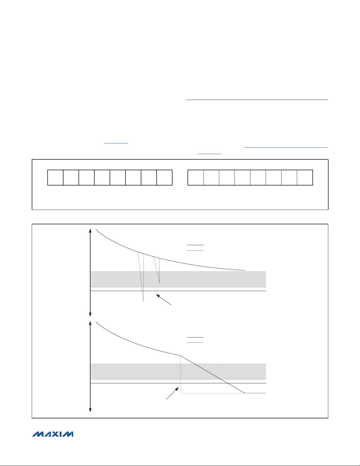
FullSOCThr Register (13h)
End-of-Charge Detection
The FullSOCThr register gates detection of end-ofcharge. SOCVF must be larger than the FullSOCThr
value before ICHGTerm is compared to the Average
Current register value. The recommended FullSOCThr
register setting for most applications is 95%. See the
ICHGTerm register description for details. The FullSOCThr
register is 70% at power-up. Figure 24 is the FullSOCThr
register format.
MSB—ADDRESS 13h LSB—ADDRESS 13h
7
6
5
4
3
2
1
2
2
2
2
2
2
2
MSb LSb MSb LSb
Figure 24. FullSOCThr Register Format (Input)
0
2
The device detects the end of a charge cycle when
the application current falls into the band set by the
ICHGTerm register value. By monitoring both the current
and average current registers, the device can reject false
end-of-charge events such as application load spikes
or early charge-source removal. See the End-of-Charge
Detection graph in the Typical Operating Characteristics
and Figure 25.
-1
2
-8
2
20 UNITS: 1%
-22-32-42-5
2
UNITS: 0.0039%
Figure 25
AVERAGE CURRENT
CHARGING
CURRENT
-6
2
-72-8
2
0mA
DISCHARGING
CHARGING
0mA
DISCHARGING
Figure 25. False End-of-Charge Events
���������������������������������������������������������������� Maxim Integrated Products 20
HIGH-CURRENT LOAD SPIKES DO NOT GENERATE END-OF-CHARGE
DETECTION BECAUSE CURRENT AND AVERAGE CURRENT READINGS
DO NOT FALL INTO THE DETECTION AREA AT THE SAME TIME.
AVERAGE CURRENT
CURRENT
EARLY CHARGER REMOVAL DOES NOT GENERATE END-OF-CHARGE
DETECTION BECAUSE CURRENT AND AVERAGE CURRENT READINGS
DO NOT FALL INTO THE DETECTION AREA AT THE SAME TIME.
1.25 x ICHGTerm
0.125 x ICHGTerm
1.25 x ICHGTerm
0.125 x ICHGTerm
Page 21

MAX17047
ModelGauge m3 Fuel Gauge
When a proper end-of-charge event is detected, the
device learns a new FullCAP register value based on
the RemCap
output. If the old FullCAP value was too
REP
high, it is adjusted downward after the last valid end-
CHARGING
0mA
DISCHARGING
of-charge detection. If the old FullCAP was too low, it is
adjusted upward to match RemCap
. This prevents
REP
the calculated state of charge from ever reporting a value
greater than 100%. See Figure 26.
AVERAGE CURRENT
CURRENT
1.25 x ICHGTerm
0.125 x ICHGTerm
CORRECT
END-OF-CHARGE
DETECTION AREA
CASE 1: OLD FullCAP TOO HIGH
CASE 2: OLD FullCAP TOO LOW
RemCap
Figure 26. FullCAP Learning at End of Charge
���������������������������������������������������������������� Maxim Integrated Products 21
NEW FullCAP
REP
Page 22

MAX17047
ModelGauge m3 Fuel Gauge
ICHGTerm Register (1Eh)
The ICHGTerm register allows the device to detect when
a charge cycle of the cell has completed. The host
should set the ICHGTerm register value equal to the
exact charge termination current used in the application.
The device detects end of charge if all the following conditions are met:
• SOCVF > FullSOCThr
• ANDICHGTermx0.125<Current<ICHGTermx1.25
• AND ICHGTerm x 0.125 < Average Current <
ICHGTerm x 1.25
Values are stored in FV. Multiply the termination current
The V_empty register sets thresholds related to empty
detection during operation. Figure 28 is the V_empty
register format.
VE8:VE0—Empty Voltage. Sets the voltage level for
detecting empty. A 10mV resolution gives a 0 to 5.11V
range. This value is written to 3.12V at power-up.
VR6:VR0—Recovery Voltage. Sets the voltage level for
clearing empty detection. Once the cell voltage rises
above this point, empty voltage detection is reenabled.
A 40mV resolution gives a 0 to 5.08V range. This value is
written to 3.68V at power-up.
V_empty Register (3Ah)
by the sense resistor to determine the desired register
value. This register has the same range and resolution
as the Current register. Figure 27 shows the ICHGTerm
register format. ICHGTerm defaults to 150mA (03C0h) at
power-up.
MSB—ADDRESS 1Eh LSB—ADDRESS 1Eh
14213212211210
S 2
MSb LSb MSb LSb
Figure 27. ICHGTerm Register Format (Input)
9
2
8
2
7
6
2
2
UNITS: 1.5625FV/R
5
2
2
SENSE
4
3
2
2
1
2
2
0
2
MSB—ADDRESS 3Ah LSB—ADDRESS 3Ah
VE8VE8VE6VE5VE4VE3VE2VE
MSb LSb MSb LSb
Figure 28. V_empty Register Format (Input)
���������������������������������������������������������������� Maxim Integrated Products 22
1
VE0VR6VR5VR4VR3VR2VR1VR
VR0 UNITS: 40mV
VE0 UNITS: 10mV
0
Page 23

MAX17047
ModelGauge m3 Fuel Gauge
Cell Characterization
Information Registers
Proper cell characterization is required to achieve accuracy. The following registers (Table 1) hold information
that must be generated through a cell-characterization
procedure. Maxim provides a cell-characterization service. Contact the factory for details.
Algorithm Configuration Registers
The following registers allow operation of the ModelGauge
m3 algorithm to be adjusted for the application. It is recommended that the default values for these registers be used.
FilterCFG Register (29h)
The FilterCFG register sets the averaging time period for
all A/D readings, for mixing OCV results and coulombcount results. It is recommended that these values are
not changed unless absolutely required by the application. Figure 29 shows the FilterCFG register format:
CURR3:CURR0—Sets the time constant for the
AverageCurrent register. The default POR value of 4h gives
a time constant of 11.25. The equation setting the period is:
AverageCurrent time constant = 175.8ms O 2
VOLT2:VOLT0—Sets the time constant for the
AverageV
register. The default POR value of 2h gives
CELL
a time constant of 45.0s. The equation setting the period is:
AverageV
time constant = 175.8ms O 2
CELL
(2+CURR)
(6+VOLT)
MIX3:MIX0—Sets the time constant for the mixing algorithm. The default POR value of Dh gives a time constant
of 12.8 hours. The equation setting the period is:
Mixing Period = 175.8ms O 2
(5+MIX)
TEMP2:TEMP0—Sets the time constant for the
AverageTemperature register. The default POR value of
1h gives a time constant of 12min. The equation setting
the period is:
AvergeTemperature time constant = 175.8ms x 2
(8 + TEMP)
X—Reserved. Do not modify.
Table 1. Cell Characterization Information
Registers
REGISTER ADDRESS
Characterization Table (48 words) 80h to AFh
FullCap 10h
DesignCap 18h
ICHGTerm 1Eh
FullCapNom 23h
RCOMP0 38h
lavg_empty 36h
TempCo 39h
QResidual 00 12h
QResidual 10 22h
QResidual 20 32h
QResidual 30 42h
MSB—ADDRESS 29h LSB—ADDRESS 29h
X X
MSb LSb MSb LSb
Figure 29. FilterCFG Register Format (Input)
TEMP 2TEMP 1TEMP
���������������������������������������������������������������� Maxim Integrated Products 23
MIX3 MIX2 MIX1 MIX0 VOLT2 VOLT1 VOLT0
0
CURR 3CURR 2CURR 1CURR
0
Page 24

MAX17047
ModelGauge m3 Fuel Gauge
RelaxCFG Register (2Ah)
The RelaxCFG register defines how the device detects
if the cell is in a relaxed state. See Figure 31. For a cell
to be considered relaxed, current flow through the cell
must be kept at a minimum while the change in the cell’s
voltage over time, dV/dt, shows little or no change. If
AverageCurrent remains below the Load threshold while
V
changes less than the dV threshold over two
CELL
consecutive periods of dt, the cell is considered relaxed.
Figure 30 shows the RelaxCFG register format:
Load6:Load0—Sets the threshold, which the
AverageCurrent register is compared against. The
AverageCurrent register must remain below this threshold value for the cell to be considered unloaded. Load is
an unsigned 7-bit value where 1 LSb = 50FV. The default
value is 800FV.
dV4:dV0—Sets the threshold, which V
against. If the cell’s voltage changes by less than dV over
two consecutive periods set by dt, the cell is considered
relaxed; dV has a range of 0 to 40mV where 1 LSb =
1.25mV. The default value is 1.75mV.
dt3:dt0—Sets the time period over which change in
V
is compared against dV. If the cell’s voltage
CELL
changes by less than dV over two consecutive periods
set by dt, the cell is considered relaxed. The default
value is 6 minutes. The comparison period is calculated
as:
Relaxation Period = 2dt O 0.1758s
MSB—ADDRESS 2Ah LSB—ADDRESS 2Ah
Load6Load5Load4Load3Load2Load1Load0dV4 dV3 dV2 dV1 dV0 dt3 dt2 dt1 dt0
MSb LSb MSb LSb
LOAD0 UNITS: 50FV/R
(5.0mAh WHEN R
SENSE
SENSE
= 0.010I)
Figure 30. RelaxCFG Register Format (Input)
is compared
CELL
0
AVERAGE
CURRENT
DISCHARGING
CELL
VOLTAGE
dV2
dt1 dt2 dt3 dt4 dt5 dt6
CELL UNLOADED
(RELAXATION BEGINS)
Figure 31. Cell Relaxation Detection
���������������������������������������������������������������� Maxim Integrated Products 24
dV3
dV4
dV5
RELAXATION LOAD THRESHOLD
dV6
FIRST
READING
BELOW
dv/dt
THRESHOLD
SECOND
READING
BELOW
dV/dt
THRESHOLD
CELL IS RELAXED
RelDt BIT SET
CELL CAPACITY IS
LEARNED
48 TO 96
MINUTES
LONG RELAXATION
RelDt2 BIT SET
Page 25

MAX17047
ModelGauge m3 Fuel Gauge
LearnCFG Register (28h)
The LearnCFG register controls all functions relating
to adaptation during operation. The LearnCFG register
default values should not be changed unless specifically
required by the application. Figure 32 is the LearnCFG
register format:
0—Bit must be written 0. Do not write 1.
1—Bit must be written 1. Do not write 0.
Filt Empty—Empty Detect Filter. This bit selects whether
empty is detected by a filtered or unfiltered voltage reading. Setting this bit to 1 causes the empty detection algorithm to use the AverageV
0 forces the empty detection algorithm to use the V
register. Setting this bit to
CELL
CELL
register. This bit is written to 0 at power-up.
LS2:LS0—Learn Stage. See Figure 3 The Learn Stage
value controls the influence of the VFG on the mixing
algorithm. At power-up, Learn Stage defaults to 0h, making the voltage fuel gauge dominate. Learn Stage then
advances to 7h over the course of two full cell cycles to
make the coulomb counter dominate. Host software can
write the Learn Stage value to 7h to advance to the final
stage at any time. Writing any value between 1h and
6h is ignored. Learn Stage reflects the D5, D6, and D7
bits of the Cycles register. Update the Cycles register
to advance to an intermediate state. For example, set
Cycles = 160% to advance to Learn Stage 5.
MiscCFG Register (2Bh)
The MiscCFG control register enables various other
functions of the device. The MiscCFG register default
values should not be changed unless specifically
required by the application. Figure 33 is the MiscCFG
register format:
0—Bit must be written 0. Do not write 1.
1—Bit must be written 1. Do not write 0.
X—Don’t Care. Bit may read 0 or 1.
SACFG1:SACFG0—SOC Alert Config. SOC Alerts can
be generated by monitoring any of the SOC registers as
follows. SACFG defaults to 00 at power-up:
0 0 SOC Alerts are generated based on the SOC
register.
0 1 SOC Alerts are generated based on the SOC
register.
1 0 SOC Alerts are generated based on the SOC
register.
1 1 SOC Alerts are generated based on the SOCVF
register.
REP
AV
MIX
MSB—ADDRESS LSB—ADDRESS
0 0 1 0 0 1 1 0 0 LS2LS1LS
MSb LSb MSb LSb
Figure 32. LearnCFG Register Format (Input/Output)
MSB—ADDRESS 2Bh LSB—ADDRESS 2Bh
0 0 X X enBi1 0 MR4MR
MSb LSb MSb LSb
Figure 33. MiscCFG Register Format (Input)
���������������������������������������������������������������� Maxim Integrated Products 25
3
MR2MR1MR01 0 0
MR0 UNITS: 6.25µV
0
Filt
1
Empty
1 1
SACFG 1SACFG
0
Page 26

MAX17047
ModelGauge m3 Fuel Gauge
MR4:MR0—Mixing Rate. This value sets the strength of
the servo mixing rate after the final mixing state has been
reached (> 2.08 complete cycles). The units are MR0 =
6.25FV, giving a range up to 19.375mA with a standard
0.010I sense resistor. Setting this value to 00000b
disables servo mixing and the IC continues with timeconstant mixing indefinitely. The default setting is 25FV
or 2.5mA with a standard sense resistor.
enBi1—Enable reset on battery-insertion detection. Set
this bit to 1 to force a reset of the fuel gauge whenever a
battery insertion is detected based on AIN pin monitoring.
This bit is written to 1 at power-up.
FSTAT Register (3Dh)
The FSTAT register is a read-only register that monitors
the status of the ModelGauge algorithm. Do not write
to this register location. Figure 34 is the FSTAT register
format:
RelDt—Relaxed cell detection. This bit is set to a 1 whenever the ModelGauge m3 algorithm detects that the cell
is in a fully relaxed state. This bit is cleared to 0 whenever
a current greater than the Load threshold is detected.
See Figure 31.
RelDt2—Long Relaxation. This bit is set to a 1 whenever
the ModelGauge m3 algorithm detects that the cell has
been relaxed for a period of 48 to 96 minutes or longer.
This bit is cleared to 0 whenever the cell is no longer in a
relaxed state. See Figure 31.
DNR—Data Not Ready. This bit is set to 1 at cell insertion and remains set until the output registers have been
updated. Afterwards, the IC clears this bit indicating the
fuel gauge calculations are now up to date. This takes
between 445ms and 1.845s depending on whether the
IC was in a powered state prior to the cell-insertion event.
EDet—Empty Detection. This bit is set to 1 when the IC
detects that the cell empty point has been reached. This
bit is reset to 0 when the cell voltage rises above the
recovery threshold. See the V_empty register for details.
X—Don’t Care. This bit is undefined and can be logic
0 or 1.
AtRate Register (04h)
The AtRate register allows host software to estimate
remaining capacity, SOC, and time to empty for a theoretical load current. Whenever the AtRate register is programmed to 0 or a positive value, the device uses A/D
measurements for determining the SOCAV, RemCapAV,
and TTE register values. Whenever the AtRate register is
programmed to a negative value indicating a hypothetical discharge current, the SOCAV, RemCapAV, and TTE
registers calculate their values for the AtRate register
theoretical current instead. The AtRate register holds a
two’s-complement 16-bit value. Do not write 8000h to
this register. Figure 35 shows the AtRate register format.
MSB—ADDRESS 3Dh LSB—ADDRESS 3Dh
X X X X X X RelDt EDet X RelDt2 X X X X X DNR
MSb LSb MSb LSb
Figure 34. FSTAT Register Format (Output)
MSB—ADDRESS 04h LSB—ADDRESS 04h
14213212211210
S 2
MSb LSb MSb LSb
Figure 35. AtRate Register Format (Input)
���������������������������������������������������������������� Maxim Integrated Products 26
9
2
8
2
7
6
2
2
20 UNITS: 1.5625FV/R
X = DON’T CARE
5
2
4
2
SENSE
3
2
2
1
2
2
0
2
Page 27

MAX17047
ModelGauge m3 Fuel Gauge
Power-Up and Power-On Reset
Any power-on reset (POR) of the device resets all
memory locations to their default POR value. This
removes any custom cell characterization and application data, affects ALRT interrupt and shutdown mode settings, and resets all learned adjustments made by the fuel
gauge. To maintain accuracy of the fuel gauge and reset
operation settings of the device, the host must reload
all application memory data and restore all learned fuelgauge information. Note that the device may take up to
445ms to completely reset operation after a POR event
occurs. See Figure 36. Saved data should not be restored
until after this period is over. The following procedure is
recommended:
1) Read Status register. If POR = 0, exit.
2) Wait 600ms for POR operation to fully complete.
3) Restore all application register values.
4) Restore fuel gauge learned-value information (see the
Save and Restore Registers section).
5) Clear POR bit.
Save and Restore Registers
The device is designed to operate outside the battery
pack and can therefore be exposed to power loss when
in the application. To prevent the loss of learned information during power cycles, a save-and-restore procedure
can be used to maintain register values in nonvolatile
memory external to the device. The registers (Table 2)
must be stored externally and then rewritten to the device
after power-up to maintain a learned state of operation.
Table 2. Save and Restore Registers
REGISTER ADDRESS
FullCap 10h
Cycles 17h
RCOMP0 38h
TempCo 39h
QResidual 00 12h
QResidual 10 22h
QResidual 20 32h
QResidual 30 42h
dQacc 45h
dPacc 46h
V
BATT
AIN
A/ D
READINGS
OUTPUT
REGISTERS
CELL
INSERTION
Figure 36. Power-Up Operation
���������������������������������������������������������������� Maxim Integrated Products 27
V
BATT
270ms
> V
DDMIN
A/D
MEASUREMENTS
COMPLETE
1.4s UNTIL NEXT TEMPERATURE READING
175ms
SOC VALUES
UPDATED
Page 28

MAX17047
ModelGauge m3 Fuel Gauge
Note that some registers are application outputs, some
registers are for internal calculations, and some are
characterization setup registers. Registers that are not
internal are described in their own sections. These values
should be stored by the application at periodic intervals.
Some recommended back-up events are:
• End-of-charge
• End-of-discharge
• Priortoapplicationenteringshutdownstate
The host is responsible for loading the default characterization data at first power-up of the device, and restoring
the default characterization data plus learned information
on subsequent power-up events.
Battery Removal and Insertion
The device detects when a cell has been removed or
inserted into the application. This allows the device to
adjust to the new cell to maintain accuracy. The removaldetection feature also allows the device to quickly warn the
host processor through interrupt of impending power loss
if enabled.
Detection occurs by monitoring the AIN pin voltage compared to the THRM pin. Whenever a cell is present, the
external resistor-divider network sets the voltage of AIN.
When the cell is removed, the remaining external resistor
pulls AIN to the THRM pin voltage level. Whenever V
< V
present in the application. If V
device determines that no cell is present at that time.
THRM
- V
, the device determines that a cell is
DETF
AIN
> V
THRM
- V
Cell Insertion (IC Already Powered)
The device is ready to detect a cell insertion if either the
ETHRM or FTHRM bits of the CONFIG register are set
to enable the THRM pin output. See Figure 37. When a
cell insertion is detected, the fuel gauge is reset and all
fuel-gauge outputs are updated to reflect the SOC of the
newly inserted cell. This process can take up to 1.845s
(FTHRM = 0) or 620ms (FTHRM = 1) from time of insertion. Note that the device uses the cell voltage as a starting point for the fuel gauge. If the cell voltage is not fully
relaxed at time of insertion, the fuel gauge begins with
DETR
AIN
, the
some initial error. See the Fuel-Gauge Learning section
for details. The host can disable this feature by clearing
the enBi1 bit in the MiscCFG register.
The device can also be configured to alert the host when
cell insertion occurs. When Bei = 1 in the CONFIG register, the device generates an interrupt on the ALRT pin
at the start of the first temperature conversion after insertion. This could take up to 1.4s to occur. This feature is
useful if the application uses more than one cell type and
the IC must be reconfigured at each insertion.
Cell Removal
The device detects a cell removal if either the ETHRM or
FTHRM bits of the CONFIG register are set to enable the
THRM pin output. Cell removal does not affect IC operation. The device continues to update fuel-gauge outputs.
The host should monitor the Br and Bst bits of the Status
register to determine if the fuel-gauge outputs are valid.
The device can also be configured to alert the host when
cell removal occurs. When Ber = 1 in the CONFIG register, the device generates an interrupt on the ALRT pin
at the start of the first temperature conversion after insertion. This could take up to 1.4s to occur. This feature is
useful if the application uses more than one cell type and
the IC must be reconfigured at each insertion.
Fast Detection of Cell Removal
The device can be configured to quickly alert the host of
impending power loss on cell removal. This fast response
allows the system to quickly and gracefully hibernate to
prevent power loss during battery swap. When Ber = 1 and
FTHRM = 1 in the CONFIG register, an interrupt on the
ALRT pin is generated within 100Fs after V
greater than V
is recommended that all other IC interrupts are disabled
to prevent the host from spending time determining the
cause of the interrupt. Fast detection of cell removal has
no affect on fuel-gauge operation, but leaving the external resistor-divider active increases current consumption
of the application. See Figure 38.
THRM
- V
. If fast detection is used, it
DETR
AIN
becomes
���������������������������������������������������������������� Maxim Integrated Products 28
Page 29

V
BATT
AIN
A/ D
READINGS
OUTPUT
REGISTERS
MAX17047
ModelGauge m3 Fuel Gauge
CELL INSERTION FROM POWERED STATE (FTHRM = 0)
UP TO 1.4s
270ms
175ms
CELL INSERTION FROM POWERED STATE (FTHRM = 1)
V
BATT
AIN
A/ D
READINGS
OUTPUT
REGISTERS
Figure 37. Operation After Cell Insertion
Figure 38
CELL
INSERTION
V
BATT
CELL
INSERTION
CELL
INSERTION
DETECTED
UP TO
175ms
CELL
INSERTION
DETECTED
CELL REMOVAL
(Ber = 1, FTHRM = 1)
MEASUREMENTS
COMPLETE
270ms
MEASUREMENTS
COMPLETE
A/D
A/D
SOC VALUES
UPDATED
175ms
SOC VALUES
UPDATED
Figure 38. Fast Detection of Cell Removal
���������������������������������������������������������������� Maxim Integrated Products 29
AIN
ALRT
OUTPUT
CELL REMOVAL INTERRUPT GENERATED
< 100µs
Page 30

MAX17047
ModelGauge m3 Fuel Gauge
Modes of Operation
The device operates in one of two power modes: active
and shutdown. While in active mode, the device operates as a high-precision battery monitor with temperature, voltage, auxiliary inputs, current, and accumulated
current measurements acquired continuously, and the
resulting values updated in the measurement registers.
READ and WRITE access is allowed only in active mode.
In shutdown mode, the LDO is disabled and all activity stops, although volatile RAM contents remain pre-
served. All A/D register and fuel-gauge output values
are maintained. There are several options for entering
shutdown:
Entering shutdown:
• SHUTDOWN command—Write the CONFIG register
SHDN = 1 through the I2C interface; wait for longer
than the SHDNTIMER register value.
• Pack removal—Pack removal detection is valid for
longer than the SHDNTIMER register value and the
CONFIG register AINSH = 1.
• I2C shutdown—I2C lines both persist low for longer
than the SHDNTIMER register value and the CONFIG
register I2CSH = 1.
• ALRT shutdown—Shutdown occurs when the ALRT
line is externally driven low for longer than the
SHDNTIMER register value (ALSH = 1 and ALRTp =
0), or the ALRT line is externally driven high for longer
than the SHDNTIMER register value (ALSH = 1 and
ALRTp = 1). See the CONFIG Register (1Dh) section.
These shutdown entry modes are all programmable
according to application. Shutdown events are gated
by the SHDNTIMER register, which allows a long delay
between the shutdown event and the actual shutdown.
By behaving this way, the device takes the best reading
of the relaxation voltage.
Exiting shutdown:
• I2C Wakeup—Any edge on SCL/SDA.
• ALRT Wakeup—Any edge on ALRT line and (ALSH =
1 or I2CSH = ALSH = 0).
• Reset—IC is power cycled.
See the Status and Configuration section for detailed
descriptions of the SHDNTIMER and CONFIG registers.
The state of the device when returning to active mode
differs depending on the triggering event. See Figure 39.
Host software can monitor the POR and Bi status bits to
determine what type of event has occurred.
Figure 39
EVENT ACTION
BATTERY INSERTION DETECTED
(THRM COMPARATOR RECOGNIZES CHANGE
FROM REMOVAL TO INSERTED STATE)
WAKE FROM SHUTDOWN STATE
2
C EDGE OR ALRT EDGE DETECTED)
(I
(RECOVERY FROM POWER LOSS)
Figure 39. MAX17047 State Based on Shutdown Exit Condition
���������������������������������������������������������������� Maxim Integrated Products 30
POWER-ON RESET
FUEL GAUGE RESTARTS FROM POINT MAINTAINED
FUEL GAUGE RESET
MaxMinVoltage REGISTER (1Bh) RESET
Cycles REGISTER (17h) RESET
ALL OTHER RAM VALUES MAINTAINED
ALL RAM VALUES MAINTAINED
WHEN SHUTDOWN WAS ENTERED
ALL RAM RESET TO DEFAULT VALUES
FUEL GAUGE RESET
STATUS
INDICATORS
DNR = 1
Bi = 1
POR = UNCHANGED
DNR = 0
Bi = UNCHANGED
POR = UNCHANGED
DNR = 1
Bi = 0
POR = 1
Page 31

MAX17047
ModelGauge m3 Fuel Gauge
ALRT Function
The Alert Threshold registers allow interrupts to be
generated by detecting a high or low voltage, a high or
low temperature, or a high or low SOC. Interrupts are
generated on the ALRT pin open-drain output driver. An
external pullup is required to generate a logic-high signal. Note that if the pin is configured to be logic-low when
inactive, the external pullup increases current drain.
The ALRTp bit in the CONFIG register sets the polarity of
the ALRT pin output. Alerts can be triggered by any of the
following conditions:
• Battery removal—(V
tery removal detection enabled (Ber = 1).
• Battery insertion—(V
tery insertion detection enabled (Bei = 1).
• Over-/undervoltage—V
(upper or lower) and alerts enabled (Aen = 1).
• Over-/undertemperature—T
(upper or lower) and alerts enabled (Aen = 1).
• Over/under SOC—S
or lower) and alerts enabled (Aen = 1).
To prevent false interrupts, the threshold registers should
be initialized before setting the Aen bit. Alerts generated by
battery insertion or removal can only be reset by clearing
> V
AIN
<V
AIN
ALRT
threshold violation (upper
ALRT
- V
THRM
THRM
- V
DETR
DETF
threshold violation
threshold violation
ALRT
) and bat-
) and bat-
the corresponding bit in the Status register. Alerts generated by a threshold-level violation can be configured to
be cleared only by software, or cleared automatically
when the threshold level is no longer violated. See the
CONFIG (1Dh) register description for details of the alert
function configuration.
The V
V
Threshold register (Figure 40) sets upper
ALRT
Threshold Register (01h)
ALRT
and lower limits that generate an ALRT pin interrupt if
exceeded by the V
register value. The upper 8
CELL
bits set the maximum value and the lower 8 bits set the
minimum value. Interrupt threshold limits are selectable
with 20mV resolution over the full operating range of the
V
register. At power-up, the thresholds default to
CELL
their maximum settings—FF00h (disabled).
The T
T
Threshold register sets upper and lower limits
ALRT
Threshold Register (02h)
ALRT
that generate an ALRT pin interrupt if exceeded by the
Temperature register value. The upper 8 bits set the maximum value and the lower 8 bits set the minimum value.
Interrupt threshold limits are stored in two’s-complement
format and are selectable with 1NC resolution over the full
operating range of the Temperature register. At powerup, the thresholds default to their maximum settings—
7F80h (disabled). Figure 41 shows the T
ALRT
Threshold
register format.
Figure 40
MAX7MAX6MAX5MAX4MAX3MAX2MAX1MAX
MSb LSb MSb LSb
Figure 40. V
Figure 41
Figure 41. T
ALRT
S MAX6MAX5MAX4MAX3MAX2MAX1MAX
MSb LSb MSb LSb
ALRT
MSB—ADDRESS 01h LSB—ADDRESS 01h
0
MIN7MIN6MIN5MIN4MIN3MIN2MIN1MIN
UNITS: 20mV
Threshold Register Format (Input)
MSB—ADDRESS 02h LSB—ADDRESS 02h
0
Threshold Register Format (Input)
���������������������������������������������������������������� Maxim Integrated Products 31
S MIN6MIN5MIN4MIN3MIN2MIN1MIN
UNITS: 1NC
0
0
Page 32

MAX17047
ModelGauge m3 Fuel Gauge
The S
S
Threshold register (Figure 42) sets upper and
ALRT
Threshold Register (03h)
ALRT
lower limits that generate an ALRT pin interrupt if exceeded
by the selected SOC
, SOCAV, SOC
REP
, or SOCVF
MIX
register values. See the SACFG bits in the MiscCFG
register description for details. The upper 8 bits set the
maximum value and the lower 8 bits set the minimum
value. Interrupt threshold limits are selectable with 1%
resolution over the full operating range of the selected
SOC register. At power-up, the thresholds default to their
maximum settings—FF00h (disabled).
Status and Configuration
The following registers control operation of the ALRT interrupt feature, control transition between active and shutdown modes of operation, and provide status updates to
the host processor.
CONFIG Register (1Dh)
The CONFIG register holds all shutdown enable, alert
enable, and temperature enable control bits. Writing a
bit location enables the corresponding function within
a 175.8ms task period. Figure 43 shows the CONFIG
register format.
0—Bit must be written 0. Do not write 1.
Ber—Enable alert on battery removal. When Ber = 1, a
battery-removal condition, as detected by the AIN pin
voltage, triggers an alert. Set to 0 at power-up. Note that
if this bit is set to 1, the ALSH bit should be set to 0 to
prevent an alert condition from causing the device to
enter shutdown mode.
Bei—Enable alert on battery insertion. When Bei = 1, a
battery-insertion condition, as detected by the AIN pin
voltage, triggers an alert. Set to 0 at power-up. Note that
if this bit is set to 1, the ALSH bit should be set to 0 to
prevent an alert condition from causing the device to
enter shutdown mode.
Aen—Enable alert on fuel-gauge outputs. When Aen =
1, violation of any of the alert threshold register values by
temperature, voltage, or SOC triggers an alert. This bit
affects the ALRT pin operation only. The Smx, Smn, Tmx,
Tmn, Vmx, and Vmn bits are not disabled. This bit is set
to 0 at power-up. Note that if this bit is set to 1, the ALSH
bit should be set to 0 to prevent an alert condition from
causing the device to enter shutdown mode.
FTHRM—Force Thermistor Bias Switch. This allows the
host to control the bias of the thermistor switch or enable
fast detection of battery removal (see the Fast Detection
of Cell Removal section). Set FTHRM = 1 to always
enable the thermistor bias switch. With a standard 10kI
thermistor, this adds an additional ~200FA to the current
drain of the circuit. This bit is set to 0 at power-up.
ETHRM—Enable Thermistor. Set to logic 1 to enable
the automatic THRM output bias and AIN measurement
every 1.4s. This bit is set to 1 at power-up.
ALSH—ALRT Shutdown. Set to logic 1 and clear the
Aen, Ber, and Bei bits to configure the ALRT pin as an
input to control shutdown mode of the device. The device
enters shutdown if the ALRT pin is held active for longer
than timeout of the SHDNTIMER register. The device
enters active mode immediately on the opposite edge of
the ALRT pin. When set to logic 0, the ALRT pin can function as an interrupt output. This bit is set to 0 at power-up.
Figure 42
MAX7MAX6MAX5MAX4MAX3MAX2MAX1MAX
MSb LSb MSb LSb
Figure 42. S
Figure 43. CONFIG Register Format (Input)
ALRT
0 SSTSVSALRTp AINSH Ten Tex SHDN I2CSH ALSH ETHRM FTHRM Aen Bei Ber
MSb LSb MSb LSb
MSB—ADDRESS 03h LSB—ADDRESS 03h
0
MIN7MIN6MIN5MIN4MIN3MIN2MIN1MIN
UNITS: 1%
Threshold Register Format (Input)
MSB—ADDRESS 1Dh LSB—ADDRESS 1Dh
���������������������������������������������������������������� Maxim Integrated Products 32
0
Page 33

MAX17047
ModelGauge m3 Fuel Gauge
Note that if this bit is set to 1, the Bei, Ber, and Aen bits
should be set to 0 to prevent an alert condition from causing the device to enter shutdown mode.
I2CSH—I2C Shutdown. Set to logic 1 to force the device
to enter shutdown mode if both SDA and SCL are held
low for more than timeout of the SHDNTIMER register.
This also configures the device to wake up on a rising
edge of either SDA or SCL. Set to 1 at power-up. Note
that if I2SCH and AINSH are both set to 0, the device
wakes up an edge of any of the SDA, SCL, or ALRT pins.
SHDN—Shutdown. Write this bit to logic 1 to force a
shutdown of the device after timeout of the SHDNTIMER
register. SHDN is reset to 0 at power-up and upon exiting
shutdown mode.
Tex—Temperature External. When set to 1, the fuel gauge
requires external temperature measurements to be written
from the host. When set to 0, measurements on the AIN
pin are converted to a temperature value and stored in the
Temperature register instead. Tex is set to 1 at power-up.
Ten—Enable Temperature Channel. Set to 1 and set
ETHRM or FTHRM to 1 to enable measurements on the
AIN pin. Ten is set to 1 at power-up.
AINSH—AIN Pin Shutdown. Set to 1 to enable device shutdown when the battery is removed. The IC enters shutdown
if the AIN pin remains high (AIN reading > V
THRM
- V
DETR
for longer than the timeout of the SHDNTIMER register. This
also configures the device to wake up when AIN is pulled low
on cell insertion. AINSH is set to 0 at power-up. Note that if
I2SCH and AINSH are both set to 0, the device wakes up an
edge of any of the SDA, SCL, or ALRT pins.
ALRTp—ALRT Pin Polarity. Regardless if ALRT is being
used as an input or output, if ALRTp = 0, the ALRT pin
is active low; if ALRTp = 1, the ALRT pin is active high.
ALRTp is set to 0 at power-up.
VS—Voltage ALRT Sticky. When VS = 1, voltage alerts
can only be cleared through software. When VS = 0, voltage alerts are cleared automatically when the threshold
is no longer exceeded. VS is set to 0 at power-up.
TS—Temperature ALRT Sticky. When TS = 1, tempera-
ture alerts can only be cleared through software. When
TS = 0, temperature alerts are cleared automatically
when the threshold is no longer exceeded. TS is set to 1
at power-up.
SS—SOC ALRT Sticky. When SS = 1, SOC alerts can
only be cleared through software. When SS = 0, SOC
alerts are cleared automatically when the threshold is no
longer exceeded. SS is set to 0 at power-up.
TIMER Register (3Eh)
This register holds timing information for the fuel gauge.
It is available to the user for debug purposes. Figure 44
shows the TIMER register format.
SHDNTIMER Register (3Fh)
The SHDNTIMER register sets the timeout period from
when a shutdown event is detected until the device
)
disables the LDO and enters low-power mode. Figure 45
shows the SHDNTIMER register format.
CTR12:CTR0—Shutdown Counter. This register counts
the total amount of elapsed time since the shutdown trigger event. This counter value stops and resets to 0 when
the shutdown timeout completes. The counter LSb is 1.4s.
Figure 44
15
2
MSb LSb MSb LSb
Figure 44. Timer Register Format (Output)
14213
2
Figure 45
THR2THR1THR0CTR12CTR11CTR10CTR9CTR
MSb LSb MSb LSb
Figure 45. SHDNTIMER Register Format (Input/Output)
MSB—Address 3Eh LSB—Address 3Eh
12
2
MSB—ADDRESS 3Fh LSB—ADDRESS 3Fh
���������������������������������������������������������������� Maxim Integrated Products 33
11
2
10
2
9
2
8
2
8
7
6
5
4
3
2
2
2
2
2
20 UNITS: 175.8ms
CTR7CTR6CTR5CTR4CTR3CTR2CTR1CTR
2
2
1
2
0
2
0
Page 34

MAX17047
ModelGauge m3 Fuel Gauge
THR2:THR0—Sets the shutdown timeout period from a
minimum of 45s to a maximum of 1.6h. The default POR
value of 7h gives a shutdown delay of 1.6h. The equation
setting the period is:
Shutdown Timeout Period = 175.8ms O 2
(8+THR)
Status Register (00h)
The Status register maintains all flags related to alert
thresholds and battery insertion or removal. Figure 46
shows the Status register format.
POR—Power-On Reset. This bit is set to a 1 when the
device detects that a software or hardware POR event
has occurred. If the host detects that the POR bit has
been set, the device should be reconfigured. See the
Power-Up and Power-On Reset section. This bit must be
cleared by system software to detect the next POR event.
POR is set to 1 at power-up.
Bst—Battery Status. This bit is set to 0 when a battery
is present in the system and set to 1 when the battery is
removed. Bst is set to 0 at power-up.
Vmn—Minimum V
set to a 1 whenever a V
the minimum V
ALRT
Threshold Exceeded. This bit is
ALRT
register reading is below
CELL
value. This bit may or may not need
to be cleared by system software to detect the next
event. See VS in the CONFIG register. Vmn is set to 0 at
power-up.
Tmn—Minimum T
Threshold Exceeded. This bit is
ALRT
set to a 1 whenever a Temperature register reading is
below the minimum T
value. This bit may or may not
ALRT
need to be cleared by system software to detect the next
event. See TS in the CONFIG register. Tmn is set to 0 at
power-up.
Smn—Minimum SOC
Threshold Exceeded. This
ALRT
bit is set to a 1 whenever SOC falls below the minimum
SOC
value. This bit may or may not need to be
ALRT
cleared by system software to detect the next event. See
SS in the CONFIG register and SACFG in the MiscCFG
register. Smn is set to 0 at power-up.
Bi—Battery Insertion. This bit is set to a 1 when the
device detects that a battery has been inserted into
the system by monitoring the AIN pin. This bit must be
cleared by system software to detect the next insertion
event. Bi is set to 0 at power-up.
Vmx—Maximum V
set to a 1 whenever a V
maximum V
value. This bit may or may not need to be
ALRT
Threshold Exceeded. This bit is
ALRT
register reading is above the
CELL
cleared by system software to detect the next event. See
VS in the CONFIG register. Vmx is set to 0 at power-up.
Tmx—Maximum T
Threshold Exceeded. This bit is
ALRT
set to a 1 whenever a Temperature register reading is
above the maximum T
value. This bit may or may
ALRT
not need to be cleared by system software to detect the
next event. See TS in the CONFIG register. Tmx is set to
0 at power-up.
Smx—Maximum SOC
Threshold Exceeded. This bit
ALRT
is set to a 1 whenever SOC rises above the maximum
SOC
value. This bit may or may not need to be
ALRT
cleared by system software to detect the next event. See
SS in the CONFIG register and SACFG in the MiscCFG
register. Smx is set to 0 at power-up.
Br—Battery Removal. This bit is set to a 1 when the system detects that a battery has been removed from the
system. This bit must be cleared by system software to
detect the next insertion event. Br is set to 0 at power-up.
X—Don’t Care. This bit is undefined and can be logic 0 or 1.
Figure 46
Br Smx Tmx Vmx Bi Smn Tmn Vmn X X X X Bst X POR X
MSb LSb MSb LSb
Figure 46. Status Register Format (Input/Output)
MSB—ADDRESS 00h LSB—ADDRESS 00h
���������������������������������������������������������������� Maxim Integrated Products 34
Page 35
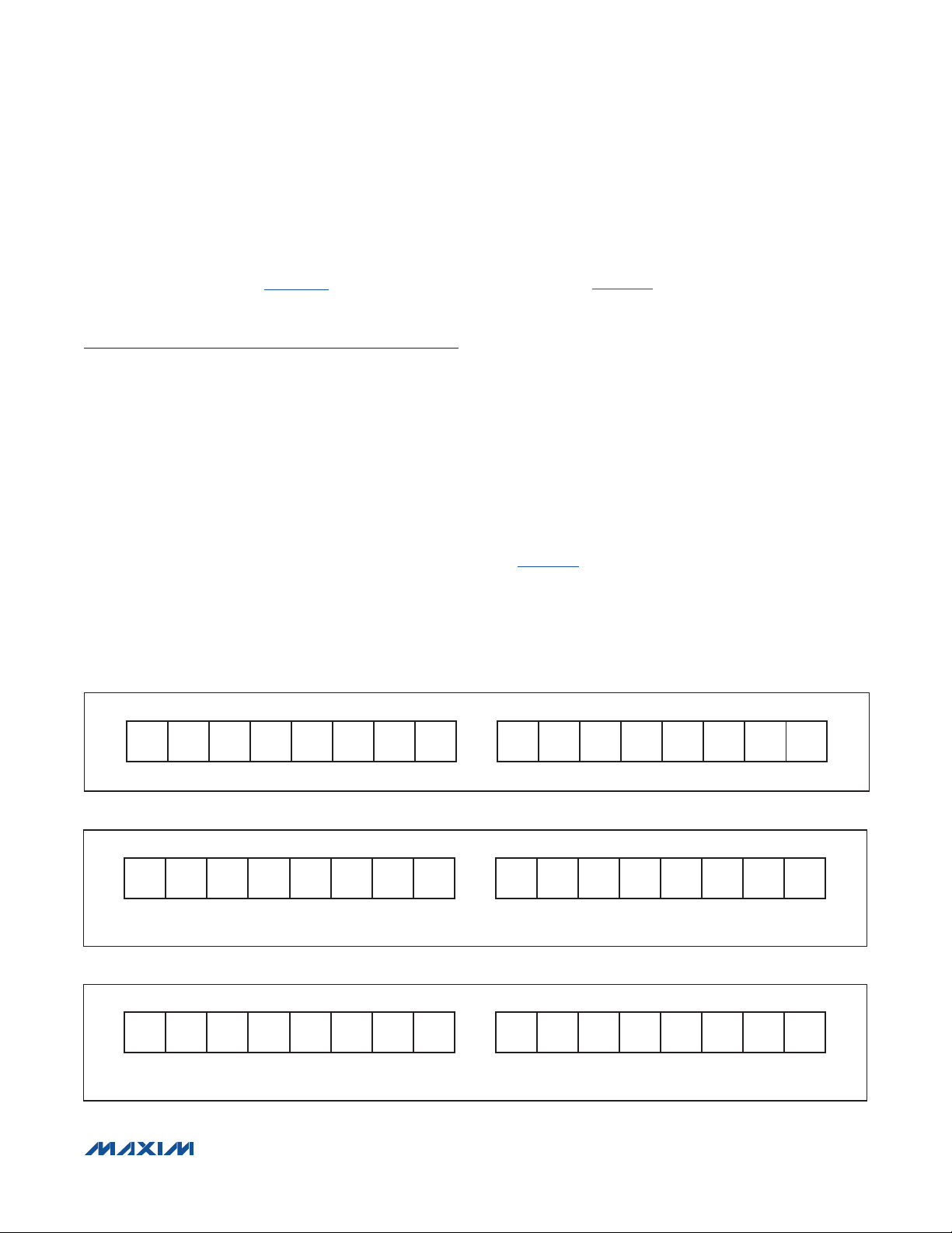
MAX17047
ModelGauge m3 Fuel Gauge
Version Register (21h)
The Version register holds a 16-bit value that indicates
the version of the device. Figure 47 shows the Version
register format.
Voltage Measurement
While in active mode, the device periodically measures
the voltage between the V
to 4.98V range. The resulting data is placed in the V
register every 175.8ms with an LSb value of 0.625mV.
Additionally, the device maintains a record of the minimum and maximum voltage measured by the device,
and an average voltage over a time period defined by
the host. Contents of the V
registers are indeterminate for the first conversion cycle
time period after device power-up. The last values of the
V
and AverageV
CELL
CELL
the device enters shutdown mode.
While in active mode, the device periodically measures the
voltage between the V
BATT
range. The resulting data is placed in the V
every 175.8ms with an LSb value of 0.625mV. Voltages
and CSP pins over a 2.5V
BATT
CELL
and AverageV
CELL
CELL
registers are maintained when
V
Register (09h)
CELL
and CSP pins over a 0 to 4.98V
register
CELL
above the maximum register value are reported as the
maximum value. The lower 3 bits of the V
don’t care bits. Figure 48 shows the V
AverageV
The AverageV
register reports an average of V
CELL
CELL
CELL
register are
CELL
register format.
Register (19h)
register readings over a configurable 12s to 24min time
period. See the FilterCFG register description for details on
setting the time filter. The resulting average is placed in the
AverageV
lower 3 bits of the AverageV
bits.The first V
up sets the starting point of the AverageV
register with an LSb value of 0.625mV. The
CELL
register reading after device power-
CELL
register are don’t care
CELL
CELL
that when a cell relaxation event is detected, the averaging period for the AverageV
register changes to the
CELL
period defined by dt3:dt0 in the RelaxCFG register. The
AverageV
register reverts back to its normal averag-
CELL
ing period when a charge or discharge current is detected. Figure 49 shows the AverageV
The MaxMinV
minimum V
CELL
MaxMinV
register maintains the maximum and
CELL
register values since the last fuel-gauge
CELL
register format.
CELL
Register (1Bh)
reset or until reset by the host software. Each time the
V
register updates, it is compared against these
CELL
CELL
filter. Note
Figure 47
15V14V13V12V11V10
V
MSb LSb MSb LSb
Figure 47. Version Register Format (Output)
Figure 48
12211210
2
MSb LSb MSb LSb
Figure 48. V
CELL
Figure 49
12211210
2
MSb LSb MSb LSb
Figure 49. AverageV
MSB—ADDRESS 21h LSB—ADDRESS 21h
MSB—ADDRESS 09h LSB—ADDRESS 09h
9
2
Register Format (Output)
MSB—ADDRESS 19h LSB—ADDRESS 19h
2
Register Format (Output)
CELL
���������������������������������������������������������������� Maxim Integrated Products 35
8
2
9
8
2
9
V
7
2
2
7
2
2
8
V
6
5
2
6
5
2
7
V
2
UNITS: 0.625mV
2
UNITS: 0.625mV
6
V
4
3
2
4
3
2
5
4
3
2
1
V
V
V
V
V
2
1
2
2
2
2
2
0
2
X X X
1
0
2
X X X
0
V
Page 36

MAX17047
ModelGauge m3 Fuel Gauge
values. If V
the minimum, the corresponding value is replaced with
the new reading. At power-up, the MaxV
to 00h (the minimum) and the MinV
FFh (the maximum). Therefore, both values are changed
to the V
CELL
software can reset this register by writing it to its powerup value of 00FFh. The maximum and minimum voltages
are each stored as 8-bit values with a 20mV resolution.
Figure 50 shows the MaxMinV
is larger than the maximum or less than
CELL
value is set
CELL
value is set to
CELL
register reading after the first update. Host
register format.
CELL
Current Measurement
Current Register readings can be adjusted by changing
the COFF and CGAIN register settings.
Additionally, the device maintains a record of the minimum and maximum current measured by the device,
and an average current over a time period defined by
the host. Contents of the Current and AverageCurrent
registers are 0000h until the first conversion cycle time
period after IC power-up. The last values of the Current
and AverageCurrent registers are maintained when the
IC enters shutdown mode.
Current Register (0Ah)
While in active mode, the device periodically measures the
While in active mode, the device periodically measures
the voltage between the CSN and CSP pins over a
Q51.2mV range. The resulting data is stored as a signed
two’s-complement value in the Current register every
175.8ms with an LSb value of 1.5625FV/R
SENSE
. All
devices are calibrated for current-measurement accuracy at the factory. However, if the application requires,
Figure 50
MAX7MAX6MAX5MAX4MAX3MAX2MAX1MAX
MSb LSb MSb LSb
MSB—ADDRESS 1Bh LSB—ADDRESS 1Bh
voltage between the CSN and CSP pins over a Q51.2mV
range. The resulting data is stored as a two’s-complement
value in the Current register every 175.8ms with an LSb value
of 1.5625FV/R
. Voltages outside the minimum and
SENSE
maximum register values are reported as the minimum or
maximum value. Figure 51 shows the Current register format
and Table 3 shows the Sample Current register conversions.
0
MIN7MIN6MIN5MIN4MIN3MIN2MIN1MIN
UNITS: 20mV
0
Figure 50. MaxMinV
Figure 51
S 2
MSb LSb MSb LSb
Figure 51. Current Register Format (Output)
Register Format (Output)
CELL
MSB—ADDRESS 0Ah LSB—ADDRESS 0Ah
14213212211210
9
2
8
2
Table 3. Sample Current Register Conversions
FUNCTION
Adjusting sense
resistor to meet
range and accuracy
requirements
Adjusting CGAIN to
keep units constant
���������������������������������������������������������������� Maxim Integrated Products 36
SENSE
RESISTOR (I)
0.005 4000h 312.50
0.010 4000h 156.25
0.020 4000h 78.125
0.005 8000h 156.25
0.010 4000h 156.25
0.020 2000h 156.25
CGAIN
REGISTER
CURRENT REGISTER
RESOLUTION (µA)
7
6
2
2
UNITS: 1.5625FV/R
5
2
CURRENT REGISTER
4
2
SENSE
RANGE (A)
Q10.24
Q5.12
Q2.56
Q5.12
Q5.12
Q5.12
3
2
1
2
2
2
MAXIMUM CELL
CAPACITY (Ah)
0
2
32.768
16.384
8.192
16.384
16.384
16.384
Page 37

MAX17047
ModelGauge m3 Fuel Gauge
AverageCurrent Register (0Bh)
The AverageCurrent register reports an average of
current-register readings over a configurable 0.7s to
6.4h time period. See the FilterCFG register description for details on setting the time filter. The resulting
average is placed in the AverageCurrent register with
an LSb value of 1.5625FV/R
. The first Current
SENSE
register reading after device power-up sets the starting point of the AverageCurrent filter. The last value
of the AverageCurrent register is maintained when the
device enters shutdown mode. Figure 52 shows the
AverageCurrent register format.
MaxMinCurrent Register (1Ch)
The MaxMinCurrent register maintains the maximum and
minimum Current register values since the last fuel gauge
reset or until cleared by host software. Each time the
Current register updates, it is compared against these
values. If the reading is larger than the maximum or less
than the minimum, the corresponding value is replaced
with the new reading. At power-up, the MaxCurrent value
Figure 52
S 2
MSB—ADDRESS 0Bh LSB—ADDRESS 0BH
14213212211210
9
2
8
2
is set to 80h (the minimum) and the MinCurrent value is
set to 7Fh (the maximum). Therefore, both values are
changed to the Current register reading after the first
update. Host software can reset this register by writing it
to its power-up value of 807Fh. The maximum and minimum voltages are each stored as two’s-complement 8-bit
values with 0.4mV/R
resolution. Figure 53 shows
SENSE
the MaxMinCurrent register format.
CGAIN Register (2Eh)/COFF Register (2Fh)
The CGAIN and COFF registers adjust the gain and offset of the current measurement result. The current measurement A/D is factory trimmed to data-sheet accuracy
without the need for the user to make further adjustments.
The default power-up settings for CGAIN and COFF
apply no adjustments to the Current register reading. For
specific application requirements, the CGAIN and COFF
registers can be used to adjust readings as follows:
Current Register = Current A/D Reading O
(CGAIN Register/16384) + (2 O COFF Register)
7
6
5
4
3
2
1
2
2
2
2
2
2
2
0
2
MSb LSb MSb LSb
UNITS: 1.5625FV/R
Figure 52. AverageCurrent Register Format (Output)
Figure 53
S MAX6MAX5MAX4MAX3MAX2MAX1MAX
MSb LSb MSb LSb
Figure 53. MaxMinCurrent Register Format (Output)
MSB—ADDRESS 1Ch LSB—ADDRESS 1Ch
0
S MIN6MIN5MIN4MIN3MIN2MIN1MIN
UNITS: 0.4mV/R
SENSE
SENSE
0
���������������������������������������������������������������� Maxim Integrated Products 37
Page 38

MAX17047
ModelGauge m3 Fuel Gauge
For easiest software compatibility between systems,
confiigure CGAIN to keep current LSB resolution at
0.15625mA. This preserves resolution of current readings
and capacities. Both these registers are signed two’s
complement. The default values of 4000h for CGAIN and
0000h for COFF preserve factory calibration and unit
values (1.5625FV). Figure 54 shows the CGAIN register
format and Figure 55 shows the COFF register format.
Temperature Measurement
While in active mode and Ten = 1 in the CONFIG register,
the device periodically measures the voltage between
the AIN and CSP pins and compares the result to the voltage of the THRM pin. The device stores the result, a ratiometric value from 0 to 100%. The resulting data is placed
in the AIN register every 1.4s with an LSB of 0.0122%.
Conversions are initiated by connecting the THRM and
VTT pins internally. This enables the active pullup to
the external voltage-divider network. After the pullup is
enabled, the device waits for a settling period of t
Figure 54
S 2
MSB—ADDRESS 2Eh LSB—ADDRESS 2Eh
0
-12-22-3
2
-42-52-6
2
PRE
prior to making measurements on the AIN pin. When
ETHRM = 1, FTHRM = 0, the active pullup is disabled
when temperature measurements are complete. This feature limits the time the external resistor-divider network
is active and lowers the total amount of energy used by
the system.
When Tex = 0 and Ten = 1 in the CONFIG register, the
device converts the AIN register to a temperature using
the temperature gain (TGAIN) and temperature offset
(TOFF) register values:
Temperature Register = (AIN Register O
TGAIN Register/16384) + (TOFF Register O 2)
The resulting value is stored in the Temperature register
each time the AIN register is updated. Additionally, the
device maintains a record of the minimum and maximum
temperature measured by the device, and an average
temperature over a time period defined by the host.
Table 4 lists the recommended TGAIN and TOFF register
values for common NTC thermistors.
-7
2
-82-92-102-112-122-132-14
2
MSb LSb MSb LSb
20 UNITS: 0.0061%
Figure 54. CGAIN Register Format (Input)
Figure 55
S 2
MSb LSb MSb LSb
Figure 55. COFF Register Format (Input)
MSB—ADDRESS 2FH LSB—ADDRESS 2Fh
14213212211210
9
2
8
2
7
2
UNITS: 3.125FV/R
6
2
2
5
SENSE
2
4
3
2
2
2
Table 4. Recommended TGAIN and TOFF Register Values for Common NTC
Thermistors
THERMISTOR
Semitec
103AT-2
Fenwal
197-103LAG-A01
TDK
Type F
���������������������������������������������������������������� Maxim Integrated Products 38
R
(kI)
25C
10 3435 E3E1h 290Eh
10 3974 E71Ch 251Ah
10 4550 E989h 22B1h
BETA RECOMMENDED TGAIN RECOMMENDED TOFF
1
2
0
2
Page 39

MAX17047
ModelGauge m3 Fuel Gauge
When Tex = 1 in the CONFIG register, the device does
not update the Temperature register based on results
from the AIN pin A/D. Instead, host software must periodically write the Temperature register with the known
application temperature to keep the fuel gauge accurate.
AIN Register (27h)
While in active mode and Ten = 1 in the CONFIG register,
the device periodically measures the voltage between
pins AIN and CSP and compares the result to the voltage
of the THRM pin. The device stores the result, a ratiometric value from 0 to 100%. The resulting data is placed
in the AIN register every 1.4s with an LSB of 0.0122%.
Contents of the AIN register are indeterminate for the
first conversion cycle time period after device power-up.
The last value of the Temperature register is maintained
when the device enters shutdown mode or if Ten = 0 in
the CONFIG register. Figure 56 shows the AIN register
format.
Temperature Register (08h)
While in active mode and Tex = 0 and Ten = 1 in the
CONFIG register, the device converts the AIN register value into a signed two’s-complement temperature
value. See the TGAIN and TOFF configuration registers.
The resulting data is placed in the Temperature register
every 1.4s with a resolution of +0.0039NC. If an 8-bit
temperature reading is desired, the host can read only
the upper byte of the Temperature register with a resolution of +1.0NC. Contents of the Temperature register are
indeterminate for the first conversion cycle time period
after device power-up. The last value of the Temperature
register is maintained when the device enters shutdown
mode. Figure 57 shows the Temperature register format.
AverageTemperature Register (16h)
The AverageTemperature register reports an average
of temperature register readings over a configurable
6min to 12h time period. See the FilterCFG register (29h)
description for details on setting the time filter. The resulting average is placed in the AverageTemperature register with an LSb value of 0.0039NC. The first Temperature
register reading after device power-up sets the starting
point of the AverageTemperature filter. The last value of
the AverageTemperature register is maintained when
the device enters shutdown mode. Figure 58 shows the
AverageTemperature register format.
MaxMinTemperature Register (1Ah)
The MaxMinTemperature register maintains the maximum and minimum Temperature register values since
the last fuel-gauge reset or until cleared by host software.
Each time the Temperature register updates, it is compared against these values. If the reading is larger than
Figure 56
-1
2
MSb LSb MSb LSb
Figure 56. AIN Register Format (Output)
Figure 57
S 2
MSb LSb MSb LSb
Figure 57. Temperature Register Format (Input/Output)
MSB—ADDRESS 27h LSB—ADDRESS 27h
-2
2
-32-42-5
2
MSB—ADDRESS 08h LSB—ADDRESS 08h
6
5
2
���������������������������������������������������������������� Maxim Integrated Products 39
4
2
2
2
3
2
-62-72-8
2
1
2
-102-112-122-13
2-92
-13
2
UNITS: 0.0122%
0
2
-12-22-3
2
-8
2
UNITS: +0.0039NC
20 UNITS: +1.0NC
-4
2
2
-52-6
X X X
-72-8
2
Page 40

MAX17047
ModelGauge m3 Fuel Gauge
the maximum or less than the minimum, the corresponding values are replaced with the new reading. At powerup, the MaxTemperature value is set to 80h (minimum)
and the MinTemperature value is set to 7Fh (maximum).
Therefore, both values are changed to the Temperature
register reading after the first update. Host software can
reset this register by writing it to its power-up value of
807Fh. The maximum and minimum temperatures are
each stored as two’s complement 8-bit values with 1NC
resolution. Figure 59 shows the MaxMinTemperature
register format.
TGAIN Register (2Ch)/TOFF Register (2Dh)
The TGAIN and TOFF registers adjust the gain and offset
of the temperature measurement A/D on the AIN pin to
convert the result to a temperature value by the following
equation:
Temperature Register = (AIN Register O
TGAIN Register/16384) + (TOFF Register O 2)
Both these registers are signed two’s complement. These
registers allow for accurate temperature conversions when
Figure 58
S 2
MSB—ADDRESS 16h LSB—ADDRESS 16h
6
5
4
3
2
1
2
2
2
2
2
0
2
using a variety of external NTC thermistors (see Table 4).
Figure 60 shows the TGAIN register format and Figure 61
shows the TOFF register format.
IC Memory Map
The device has a 256-word linear memory space containing all user-accessible registers. All registers are
16 bits wide and are read and written as 2-byte values.
When the MSB of a register is read, the MSB and LSB
are latched simultaneously and held for the duration of
the Read Data command. This prevents updates to the
LSB during the read, ensuring synchronization between
the 2 register bytes.
All locations are volatile RAM and lose their data in the
event of power loss. Data is retained during device
shutdown. Each register has a power-on-reset value that
it defaults to at power-up. Word addresses designated
as reserved return an undetermined when read. These
locations
should not be written.
-12-22-32-4
2
-52-6
2
-7
2
-8
2
MSb LSb MSb LSb
-8
2
UNITS: +0.0039NC
20 UNITS: +1.0NC
Figure 58. AverageTemperature Register Format (Output)
Figure 59
S MAX6MAX5MAX4MAX3MAX2MAX1MAX
MSb LSb MSb LSb
Figure 59. MaxMinTemperature Register Format (Output)
Figure 60
S 2
MSb LSb MSb LSb
Figure 60. TGAIN Register Format (Input)
MSB—ADDRESS 1Ah LSB—ADDRESS 1Ah
0
MSB—ADDRESS 2Ch LSB—ADDRESS 2Ch
14213212211210
���������������������������������������������������������������� Maxim Integrated Products 40
9
2
8
2
S MIN6MIN5MIN4MIN3MIN2MIN1MIN
UNITS: +1NC
7
6
5
4
3
2
2
2
20 UNITS: +1NC/64
2
2
2
2
0
1
2
0
2
Page 41

MAX17047
ModelGauge m3 Fuel Gauge
Figure 61
S 2
MSB—ADDRESS 2Dh LSB—ADDRESS 2Dh
6
6
5
4
3
2
2
2
2
2
2
1
2
0
2
-12-22-32-4
2
MSb LSb MSb LSb
-7
2
UNITS: +0.0078NC
Figure 61. TOFF Register Format (Input)
Table 5. Device Memory Map
ADDRESS
(HEX)
REGISTER NAME
00h Status
01h V
02h T
03h S
ALRT
ALRT
ALRT
Threshold
Threshold
Threshold
04h AtRate
05h RemCap
06h SOC
REP
REP
07h Age
08h Temperature
09h V
CELL
0Ah Current
0Bh AverageCurrent
0Ch RESERVED
0Dh SOC
0Eh SOC
0Fh RemCap
MIX
AV
MIX
10h FullCAP
11h TTE
12h QResidual 00
13h FullSOCThr
14h–15h RESERVED
16h AverageTemperature
17h Cycles
18h DesignCap
19h AverageV
CELL
1Ah MaxMinTemperature
1Bh MaxMinV
CELL
1Ch MaxMinCurrent
1Dh CONFIG
1Eh ICHGTerm
1Fh RemCap
AV
20h RESERVED
21h Version
A/D
MEASURE
ü
ü
ü
ü
ü
ü
ü
ü
ü
ALERT/
STATUS
ü
ü
ü
ü
ü
ü
MG m3
DATA
APP
ü
ü
ü
MG m3
CELL
DATA
MG m3
CONFIG
ü
ü ü
MG m3
SAVE AND
RESTORE
ü ü
ü ü
MG m3
OUTPUT
-52-6
2
ü
ü
ü
ü
ü
ü
ü
ü
-7
2
POR
VALUE
READ/
WRITE
0002h R/W
FF00h R/W
7F80h R/W
FF00h R/W
0000h R/W
03E8h R
3200h R
6400h R
1600h R/W
B400h R
0000h R
0000h R
— —
3200h R
3200h R
03E8h R
07D0h R/W
0000h R
1E2Fh R/W
4600h R/W
— —
1600h R
0000h R/W
07D0h R/W
B400h R
807Fh R/W
00FFh R/W
807Fh R/W
2350h R/W
03C0h R/W
03E8h R
— —
00ACh R
���������������������������������������������������������������� Maxim Integrated Products 41
Page 42

Table 5. Device Memory Map (continued)
MAX17047
ModelGauge m3 Fuel Gauge
ADDRESS
(HEX)
22h QResidual 10
23h FullCapNom
24h TempNom
25h TempLim
26h RESERVED
27h AIN
28h LearnCFG
29h FilterCFG
2Ah RelaxCFG
2Bh MiscCFG
2Ch TGAIN
2Dh TOFF
2Eh CGAIN
2Fh COFF
30h–31h RESERVED
32h QResidual 20
33h–35h RESERVED
36h Iavg_empty
37h FCTC
38h RCOMP0
39h TempCo
3Ah V_empty
3Bh RESERVED
3Ch RESERVED
3Dh FSTAT
3Eh TIMER
3Fh SHDNTIMER
40h–41h RESERVED
42h QResidual 30
43h–44h RESERVED
45h dQacc
46h dPacc
47h–4Ch RESERVED
4Dh QH
4Eh–7Fh RESERVED
80h–AFh
B0h–FAh RESERVED
FBh VFOCV
FCh–FEh RESERVED
FFh SOC
REGISTER NAME
Characterization
Table
VF
A/D
MEASURE
ü
ü
ü
ü
ü
ALERT/
STATUS
ü
ü
MG m3
APP
DATA
ü
MG m3
CELL
DATA
MG m3
CONFIG
ü ü
ü ü
ü
ü
ü
ü
ü
ü
ü ü
ü
ü
ü ü
ü ü
ü ü
ü
MG m3
SAVE AND
RESTORE
ü
ü
MG m3
OUTPUT
ü
ü
ü
ü
POR
VALUE
1E00h R/W
07D0h R/W
1400h R/W
2305h R/W
88D0h R
2603h R/W
4EA4h R/W
203Bh R/W
0870h R/W
E3E1h R/W
290Eh R/W
4000h R/W
0000h R/W
1306h R/W
0780h R/W
05E0h R/W
004Bh R/W
262Bh R/W
9C5Ch R/W
0001h R
0000h R
E000h R/W
0C00h R/W
007Dh R/W
0C80h R/W
0000h R/W
N/A R/W
0000h R
0000h R
READ/
WRITE
— —
— —
— —
— —
— —
— —
— —
— —
— —
— —
— —
���������������������������������������������������������������� Maxim Integrated Products 42
Page 43

MAX17047
ModelGauge m3 Fuel Gauge
2-Wire Bus System
The 2-wire bus system supports operation as a slaveonly device in a single or multislave, and single or
multimaster system. Up to 128 slave devices may share
the bus by uniquely setting the 7-bit slave address. The
2-wire interface consists of a serial data line (SDA) and
serial clock line (SCL). SDA and SCL provide bidirectional communication between the MAX17047 slave
device and a master device at speeds up to 400kHz. The
device’s SDA pin operates bidirectionally, that is, when
the device receives data, SDA operates as an input, and
when the device returns data, SDA operates as an opendrain output, with the host system providing a resistive
pullup. The device always operates as a slave device,
receiving and transmitting data under the control of a
master device. The master initiates all transactions on the
bus and generates the SCL signal, as well as the START
and STOP bits, which begin and end each transaction.
Bit Transfer
One data bit is transferred during each SCL clock cycle,
with the cycle defined by SCL transitioning low to high
and then high to low. The SDA logic level must remain
stable during the high period of the SCL clock pulse.
Any change in SDA when SCL is high is interpreted as a
START or STOP control signal.
Bus Idle
The bus is defined to be idle, or not busy, when no master device has control. Both SDA and SCL remain high
when the bus is idle. The STOP condition is the proper
method to return the bus to the idle state.
bits. To generate an Acknowledge, the receiving device
must pull SDA low before the rising edge of the acknowledge-related clock pulse (ninth pulse) and keep it low
until SCL returns low. To generate a No Acknowledge
(also called NACK), the receiver releases SDA before
the rising edge of the acknowledge-related clock pulse
and leaves SDA high until SCL returns low. Monitoring
the acknowledge bits allows for detection of unsuccessful data transfers. An unsuccessful data transfer can
occur if a receiving device is busy or if a system fault has
occurred. In the event of an unsuccessful data transfer,
the bus master should reattempt communication.
Data Order
A byte of data consists of 8 bits ordered most significant
bit (MSb) first. The least significant bit (LSb) of each byte
is followed by the Acknowledge bit. Device registers
composed of multibyte values are ordered least significant byte (LSB) first.
Slave Address
A bus master initiates communication with a slave device
by issuing a START condition followed by a Slave Address
(SAddr) and the read/write (R/W) bit. When the bus is idle,
the device continuously monitors for a START condition
followed by its slave address. When the device receives a
slave address that matches the value in its Programmable
Slave Address register, it responds with an Acknowledge
bit during the clock period following the R/W bit. The 7-bit
Programmable Slave Address register is factory programmed and cannot be changed by the user.
IC SLAVE ADDRESS
0110110
START and STOP Conditions
The master initiates transactions with a START condition
(S), by forcing a high-to-low transition on SDA while SCL
is high. The master terminates a transaction with a STOP
condition (P), a low-to-high transition on SDA while SCL
is high. A Repeated START condition (Sr) can be used
in place of a STOP then START sequence to terminate
one transaction and begin another without returning the
bus to the idle state. In multimaster systems, a Repeated
START allows the master to retain control of the bus. The
START and STOP conditions are the only bus activities in
which the SDA transitions when SCL is high.
Acknowledge Bits
Each byte of a data transfer is acknowledged with an
Acknowledge bit (A) or a No Acknowledge bit (N). Both
the master and the device slave generate acknowledge
���������������������������������������������������������������� Maxim Integrated Products 43
Read/Write Bit
The R/W bit following the slave address determines the
data direction of subsequent bytes in the transfer. R/W
= 0 selects a write transaction, with the following bytes
being written by the master to the slave. R/W = 1 selects
a read transaction, with the following bytes being read
from the slave by the master.
Bus Timing
The device is compatible with any bus timing up to
400kHz. No special configuration is required to operate
at any speed.
2-Wire Command Protocols
The command protocols involve several transaction
formats. The simplest format consists of the master
writing the START bit, slave address, R/W bit, and then
Page 44

MAX17047
ModelGauge m3 Fuel Gauge
monitoring the acknowledge bit for presence of the
device. More complex formats such as the write Data,
read Data, and Function command protocols write data,
read data, and execute device-specific operations,
respectively. All bytes in each command format require
the slave or the host system to return an Acknowledge bit
before continuing with the next byte. Each function command definition outlines the required transaction format.
Table 6 applies to the transaction formats.
Basic Transaction Formats
Write: S SAddr W A MAddr A DataL A DataH A P
A write transaction transfers 1 or more data bytes to the
device. The data transfer begins at the memory address
supplied in the MAddr byte. Control of the SDA signal is
retained by the master throughout the transaction, except
for the Acknowledge cycles.
Read: S SAddr W A MAddr A Sr SAddr R A DataL A DataH N P
write Portion read Portion
A read transaction transfers one or more words from the
IC. Read transactions are composed of two parts, a write
portion followed by a read portion, and are therefore
inherently longer than a write transaction. The write portion communicates the starting point for the read operation. The read portion follows immediately, beginning with
a Repeated START, Slave Address with R/W set to a 1.
Control of SDA is assumed by the IC beginning with the
Slave Address Acknowledge cycle. Control of the SDA
signal is retained by the device throughout the transaction, except for the Acknowledge cycles. The master
Table 6. 2-Wire Protocol Key
KEY DESCRIPTION KEY DESCRIPTION
S START bit Sr Repeated START
SAddr
FCmd
MAddr
Data
Slave Address
(7 bit)
Function Command
byte
Memory Address
byte
Data byte written by
Master
Acknowledge bit—
A
Master
No Acknowledge—
N
Master
W R/W bit = 0
R R/W bit = 1
P STOP bit
Data
Data byte returned
by Slave
Acknowledge bit—
A
Slave
No Acknowledge—
N
Slave
indicates the end of a read transaction by responding
to the last byte it requires with a No Acknowledge. This
signals the device that control of SDA is to remain with
the master following the Acknowledge clock.
Write Data Protocol
The write Data protocol is used to write to register and
shadow RAM data to the IC starting at memory address
MAddr. Data0 represents the data written to MAddr,
Data1 represents the data written to MAddr + 1, and
DataN represents the last data byte written to MAddr +
N. The master indicates the end of a write transaction by
sending a STOP or Repeated START after receiving the
last acknowledge bit:
S SAddr W A MAddr A DataL0 A DataH0 A DataL1
A DataH1 A … DataLN A DataHN A P
The MSb of the data to be stored at address MAddr
can be written immediately after the MAddr byte is
acknowledged. Because the address is automatically
incremented after the least significant bit (LSb) of each
byte is received by the device, the MSB of the data at
address MAddr + 1 can be written immediately after the
acknowledgment of the data at address MAddr. If the
bus master continues an autoincremented write transaction beyond address FFh, the device ignores the data.
Data is also ignored on writes to read-only addresses
but not reserved addresses. Do not write to reserved
address locations.
Read Data Protocol
The read data protocol is used to read register and
shadow RAM data from the device starting at memory
address specified by MAddr. Data0 represents the data
byte in memory location MAddr, Data1 represents the
data from MAddr + 1, and DataN represents the last byte
read by the master:
S SAddr W A MAddr A Sr SAddr R A DataL0 A
DataH0 A DataL1 A DataH1 A …DataLN N DataHN N P
Data is returned beginning with the most significant bit
(MSb) of the data in MAddr. Because the address is
automatically incremented after the LSb of each byte
is returned, the MSb of the data at address MAddr +
1 is available to the host system immediately after the
acknowledgment of the data at address MAddr. If the
bus master continues to read beyond address FFh, the
device outputs data values of FFh. Addresses labeled
Reserved in the memory map return undefined data. The
bus master terminates the read transaction at any byte
boundary by issuing a No Acknowledge followed by a
STOP or Repeated START.
���������������������������������������������������������������� Maxim Integrated Products 44
Page 45

MAX17047
ModelGauge m3 Fuel Gauge
Ordering Information
PART TEMP RANGE PIN-PACKAGE
MAX17047G+ -40°C to +85°C 10 TDFN-EP*
MAX17047G+T10 -40°C to +85°C 10 TDFN-EP*
+Denotes a lead(Pb)-free/RoHS-compliant package.
T = Tape and reel.
*EP = Exposed pad.
Package Information
For the latest package outline information and land patterns
(footprints), go to www.maxim-ic.com/packages. Note that a
“+”, “#”, or “-” in the package code indicates RoHS status only.
Package drawings may show a different suffix character, but
the drawing pertains to the package regardless of RoHS status.
PACKAGE
TYPE
10 TDFN-EP T1033+1
PACKAGE
CODE
OUTLINE
NO.
21-0137 90-0003
LAND
PATTERN NO.
���������������������������������������������������������������� Maxim Integrated Products 45
Page 46

MAX17047
ModelGauge m3 Fuel Gauge
Revision History
REVISION
NUMBER
0 9/11 Initial release —
REVISION
DATE
DESCRIPTION
PAGES
CHANGED
Maxim cannot assume responsibility for use of any circuitry other than circuitry entirely embodied in a Maxim product. No circuit patent licenses are implied.
Maxim reserves the right to change the circuitry and specifications without notice at any time. The parametric values (min and max limits) shown in the Electrical
Characteristics table are guaranteed. Other parametric values quoted in this data sheet are provided for guidance.
Maxim Integrated Products, 120 San Gabriel Drive, Sunnyvale, CA 94086 408-737-7600 46
©
2011 Maxim Integrated Products Maxim is a registered trademark of Maxim Integrated Products, Inc.
 Loading...