

Page 1
General Description
The MAX17030/MAX17036 are 3/2-phase interleaved
Quick-PWM™ step-down VID power-supply controllers
for IMVP-6.5 notebook CPUs. Two integrated drivers and
the option to drive a third phase using an external driver
such as the MAX8791 allow for a flexible 3/2-phase configuration depending on the CPU being supported.
True out-of-phase operation reduces input ripple-current
requirements and output-voltage ripple while easing
component selection and layout difficulties. The QuickPWM control provides instantaneous response to fast
load-current steps. Active voltage positioning reduces
power dissipation and bulk output capacitance requirements and allows ideal positioning compensation for tantalum, polymer, or ceramic bulk output capacitors.
The MAX17030/MAX17036 are intended for bucking
down the battery directly to create the core voltage.
The single-stage conversion method allows this device
to directly step down high-voltage batteries for the
highest possible efficiency.
A slew-rate controller allows controlled transitions
between VID codes. A thermistor-based temperature
sensor provides programmable thermal protection. An
output current monitor provides an analog current output proportional to the sum of the inductor currents,
which in steady state is the same as the current consumed by the CPU.
Applications
IMVP-6.5 SV and XE Core Power Supplies
High-Current Voltage-Positioned Step-Down
Converters
3 to 4 Li+ Cells Battery to CPU Core Supply
Converters
Notebooks/Desktops/Servers
Features
o Triple/Dual-Phase Quick-PWM Controllers
o 2 Internal Drivers + 1 External Driver
o ±0.5% V
OUT
Accuracy Over Line, Load, and
Temperature
o 7-Bit IMVP-6.5 DAC
o Dynamic Phase Selection Optimizes Active/Sleep
Efficiency
o Transient Phase Overlap Reduces Output
Capacitance
o Transient Suppression Feature (MAX17036 Only)
o Integrated Boost Switches
o Active Voltage Positioning with Adjustable Gain
o Accurate Lossless Current Balance and
Current Limit
o Remote Output and Ground Sense
o Adjustable Output Slew-Rate Control
o Power-Good (IMVPOK), Clock Enable (CLKEN),
and Thermal-Fault (VRHOT) Outputs
o IMVP-6.5 Power Sequencing and Timing
Compliant
o Output Current Monitor (IMON)
o Drives Large Synchronous Rectifier FETs
o 7V to 26V Battery Input Range
o Adjustable Switching Frequency (600kHz max)
o Undervoltage, Overvoltage, and Thermal-Fault
Protection
MAX17030/MAX17036
1/2/3-Phase Quick-PWM
IMVP-6.5 VID Controllers
________________________________________________________________
Maxim Integrated Products
1
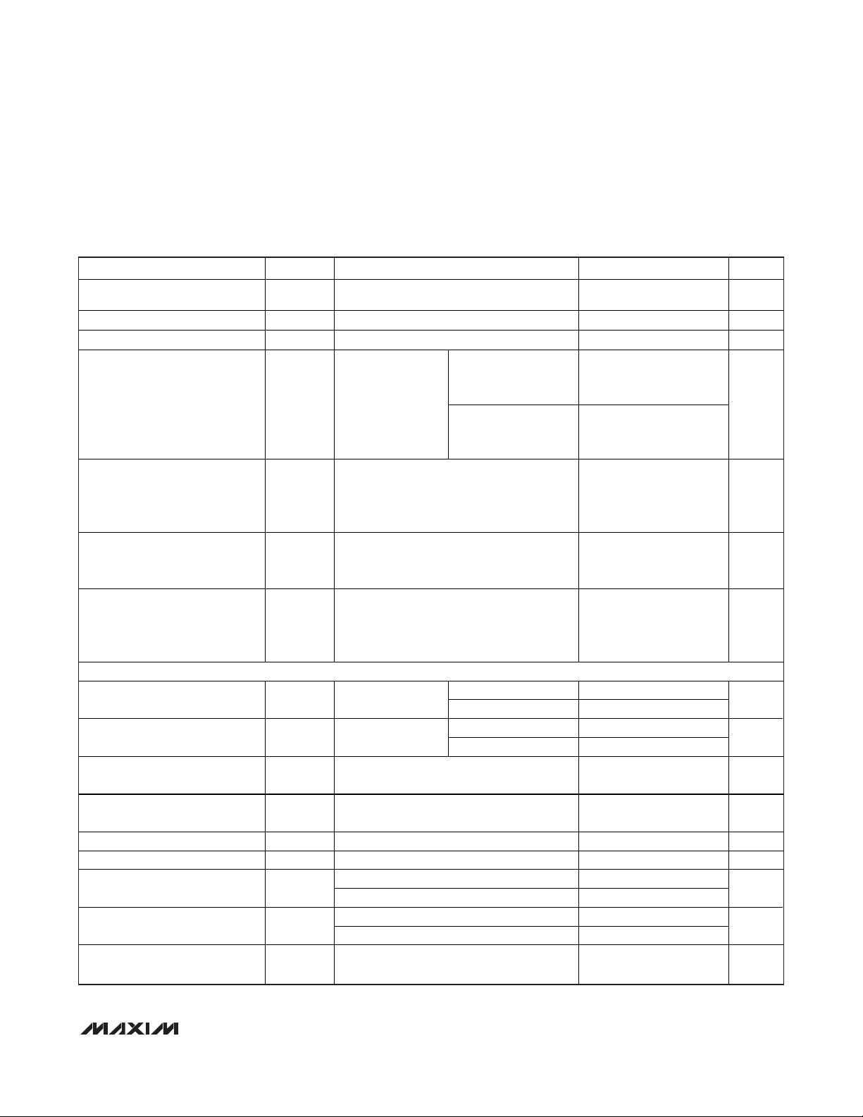
Pin Configuration
Ordering Information
19-4577; Rev 0; 4/09
For pricing, delivery, and ordering information, please contact Maxim Direct at 1-888-629-4642,
or visit Maxim’s website at www.maxim-ic.com.
EVALUATION KIT
AVAILABLE
PART TEMP RANGE PIN-PACKAGE
MAX17030GTL+ -40°C to +105°C 40 TQFN-EP*
MAX17036GTL+ -40°C to +105°C 40 TQFN-EP*
+
Denotes a lead-free(Pb)/RoHS-compliant package.
*
EP = Exposed pad.
Quick-PWM is a trademark of Maxim Integrated Products, Inc.
TOP VIEW
PGD_IN
CSP1
CSN1
BST1
LX1
31
32
D0
33
D1
34
D2
35
D3
36
D4
37
D5
38
D6
39
40
+
12 4 567
3
CSP3
CSN3
DD
DL1
V
VRHOT
ILIM
DL2
25
CC
V
TIME
DH1
27282930 26 24 23 22
MAX17030
MAX17036
IMON
THRM
THIN QFN
5mm x 5mm
DH2
LX2
BST2
21
8910
FB
FBAC
GNDS
20
19
18
17
16
15
14
13
12
11
PWM3
DRSKP
PWRGD
CLKEN
TON
PSI
DPRSLPVR
SHDN
CSP2
CSN2
Page 2
MAX17030/MAX17036
1/2/3-Phase Quick-PWM
IMVP-6.5 VID Controllers
2 _______________________________________________________________________________________
ABSOLUTE MAXIMUM RATINGS
(Note 1)
ELECTRICAL CHARACTERISTICS
(Circuit of Figure 1, VIN= 10V, VCC= VDD= V
SHDN
= V
PGD_IN
= V
PSI
= V
ILIM
= 5V, V
DPRSLPVR
= V
GNDS
= 0, V
CSP_
= V
CSN_
=
1.0000V, FB = FBAC, R
FBAC
= 3.57kΩ from FBAC to CSN_, [D6–D0] = [0101000]; TA= 0°C to +85°C, unless otherwise noted.
Typical values are at T
A
= +25°C.)
Stresses beyond those listed under “Absolute Maximum Ratings” may cause permanent damage to the device. These are stress ratings only, and functional
operation of the device at these or any other conditions beyond those indicated in the operational sections of the specifications is not implied. Exposure to
absolute maximum rating conditions for extended periods may affect device reliability.
VCC, VDDto GND .....................................................-0.3V to +6V
D0–D6, PGD_IN, PSI, DPRSLPVR to GND ...............-0.3V to +6V
CSP_, CSN_, THRM, ILIM to GND............................-0.3V to +6V
PWRGD, CLKEN, VR_HOT to GND..........................-0.3V to +6V
FB, FBAC, IMON, TIME to GND .................-0.3V to (V
CC
+ 0.3V)
SHDN to GND (Note 2)...........................................-0.3V to +30V
TON to GND ...........................................................-0.3V to +30V
GNDS to GND .......................................................-0.3V to +0.3V
DL1, DL2, PWM3, DRSKP to GND .............-0.3V to (V
DD
+ 0.3V)
BST1, BST2 to GND ...............................................-0.3V to +36V
BST1, BST2 to V
DD
.................................................-0.3V to +30V
LX1 to BST1..............................................................-6V to +0.3V
LX2 to BST2..............................................................-6V to +0.3V
DH1 to LX1 ..............................................-0.3V to (V
BST1
+ 0.3V)
DH2 to LX2 ..............................................-0.3V to (V
BST2
+ 0.3V)
Continuous Power Dissipation (40-pin, 5mm x 5mm TQFN)
Up to +70°C ..............................................................1778mW
Derating above +70°C ..........................................22.2mW/°C
Operating Temperature Range .........................-40°C to +105°C
Junction Temperature......................................................+150°C
Storage Temperature Range .............................-65°C to +165°C
Lead Temperature (soldering, 10s) .................................+300°C
Note 1: Absolute Maximum Ratings valid using 20MHz bandwidth limit.
Note 2: SHDN might be forced to 12V for the purpose of debugging prototype breadboards using the no-fault test mode. Internal
BST switches are disabled as well. Use external BST diodes when SHDN is forced to 12V.
PWM CONTROLLER
Input Voltage Range
FB Output Voltage Accuracy V
Boot Voltage V
Line Regulation Error VCC = 4.5V to 5.5V, VIN = 4.5V to 26V 0.1 %
FB Input Bias Current TA = +25°C -0.1 +0.1 µA
GNDS Input Range -200 +200 mV
GNDS Gain A
GNDS Input Bia s Current I
TIME Regulation Voltage V
TIME Slew-Rate Accurac y
PARAMETER SYMBOL CONDITIONS MIN TYP MAX UNITS
FB
BOOT
GNDS
TA = +25°C -0.5 +0.5 µA
GNDS
R
TIME
VCC, V
V
Measured at FB
with respect to
GNDS;
includes loadregulation error
(Note 3)
1.094 1.100 1.106 V
V
R
R
178k (5mV/µs nominal)
Soft-start and soft-shutdown:
R
178k (1.25mV/µs nominal)
DD
7 26
IN
/V
OUT
GNDS
= 147k 1.985 2.000 2.015 V
TIME
= 147k (6.08mV/µs nominal) -10 +10
TIME
= 35.7k (25mV/µs nominal) to
TIME
= 35.7k (6.25mV/µs nominal) to
TIME
DAC codes from
0.8125V to 1.5000V
DAC codes from
0.3750V to 0.8000V
DAC codes from
0 to 0.3625V
0.97 1.00 1.03 V/V
4.5 5.5
-0.5 +0.5 %
-7 +7
-20 +20
-15 +15
-20 +20
V
mV
%
Page 3
MAX17030/MAX17036
1/2/3-Phase Quick-PWM
IMVP-6.5 VID Controllers
_______________________________________________________________________________________ 3
ELECTRICAL CHARACTERISTICS (continued)
(Circuit of Figure 1, VIN= 10V, VCC= VDD= V
SHDN
= V
PGD_IN
= V
PSI
= V
ILIM
= 5V, V
DPRSLPVR
= V
GNDS
= 0, V
CSP_
= V
CSN_
=
1.0000V, FB = FBAC, R
FBAC
= 3.57kΩ from FBAC to CSN_, [D6–D0] = [0101000]; TA= 0°C to +85°C, unless otherwise noted.
Typical values are at T
A
= +25°C.)
PARAMETER SYMBOL CONDITIONS MIN TYP MAX UNITS
On-Time Accuracy t
Minimum Off-Time t
TON Shutdown Input Current I
BIAS CURRENTS
Quie sc ent Supply Current (VCC) I
Quie sc ent Supply Current (VDD) I
Shutdown Supply C urrent (VCC) I
Shutdown Supply C urrent (VDD) I
FAULT PROTECTION
Output Overvoltage-Protection
Threshold
Output OvervoltagePropagation Dela y
Output UndervoltageProtection Threshold
Output UndervoltagePropagation Dela y
CLKEN Startup Delay and
Boot Time Period
ON
OFF(MIN)
TON,SDN
CC
DD
CC, SDN
DD, SDN
V
OVP
t
OVP
V
UVP
t
UVP
t
BOOT
VIN = 10V,
= 1.0V,
V
FB
measured at
DH1, DH2,
and PWM3
(Note 4)
Measured at DH1, DH2, and PWM3 (Note 4) 300 375 ns
SHDN = GND, VIN = 26V, VCC = VDD = 0
or 5V, T
A
Measured at VCC, V
forced above the regulation point
Mea sured at VDD, V
above the regulation point, T
Mea sured at VCC, SHDN = GND, TA = +25°C 0.01 1 µA
Mea sured at VDD, SHDN = GND, TA = +25°C 0.01 1 µA
Skip mode after output reache s the
regulation voltage or PWM mode;
measured at FB with respect to the voltage
target set by the VID code (see Table 4)
Soft-start, soft-shutdown, skip mode, and
output have not reached the regulation
voltage; measured at FB
Min imum OVP threshold; measured at FB 0.8
FB forced 25mV above trip thresho ld 10 µs
Measured at FB with respect to the voltage
target set by the VID code (see Table 4)
FB forced 25mV below trip threshold 10 µs
Measured from the time when FB reaches
the boot target vo ltage (Note 3)
= +25°C
R
per phase), 167ns nominal
R
per phase), 333ns nominal
R
per phase), 500ns nominal
= 96.75k (600kHz
TON
= 200k (300kHz
TON
= 303.25k (200kHz
TON
DPRSLPVR
DPRSLPVR
= 5V, FB
= 0, FB forced
= +25°C
A
-15 +15
-10 +10
-15 +15
0.01 0.1 µA
3.5 7 mA
0.02 1 µA
250 300 350 mV
1.45 1.50 1.55
-450 -400 -350 mV
20 60 100 µs
%
V
Page 4
MAX17030/MAX17036
1/2/3-Phase Quick-PWM
IMVP-6.5 VID Controllers
4 _______________________________________________________________________________________
ELECTRICAL CHARACTERISTICS (continued)
(Circuit of Figure 1, VIN= 10V, VCC= VDD= V
SHDN
= V
PGD_IN
= V
PSI
= V
ILIM
= 5V, V
DPRSLPVR
= V
GNDS
= 0, V
CSP_
= V
CSN_
=
1.0000V, FB = FBAC, R
FBAC
= 3.57kΩ from FBAC to CSN_, [D6–D0] = [0101000]; TA= 0°C to +85°C, unless otherwise noted.
Typical values are at T
A
= +25°C.)
PARAMETER SYMBOL CONDITIONS MIN TYP MAX UNITS
PWRGD Startup Dela y
CLKEN and PWRGD Threshold
CLKEN and PWRGD Delay
CLKEN and PWRGD Transition
Blank ing Time (VID Transitions)
t
BLANK
CLKEN, PWRGD Output
Low Voltage
CLKEN, PWRGD Leakage
Current
CSN1 Pulldown Resi stance in
UVLO and Shutdown
VCC Undervoltage-Lockout
Threshold
V
UVLO(VCC)
THERMAL PROTECTION
VRHOT Trip Threshold
VRHOT Delay t
VRHOT Output On-Resistance R
VRHOT
ON(VRHOT)
VRHOT Leakage Current High-Z state, VRHOT forced to 5V, TA = +25°C 1 µA
THRM Input Leakage I
Thermal-Shutdown Threshold T
THRM
SHDN
V
VALLEY CURRENT LIMIT, DROOP, CURRENT BALANCE, AND CURRENT MONITOR
Current-Limit Threshold Voltage
(Positive)
Current-Limit Threshold Voltage
(Negative) Accuracy
Current-Limit Threshold Voltage
(Zero Crossing)
V
LIMIT
V
LIMIT(NEG) VCSP_
V
ZX
CSP_, CSN_ Common-Mode
Input Range
Measured at startup from the time when
CLKEN goes low
Measured at FB
with respect to the
voltage target set
by the VID code
(see Table 4), 20mV
hysteresis (typ)
FB forced 25mV out side the PWRGD trip
thresholds
Measured from the time when FB reaches
the target voltage (Note 3)
Low state, I
High-Z state, pin forced to 5V, T
SHDN = GND, measured after softshutdown completed (DL = low)
Rising edge, 65mV typical hy steresi s,
controller disabled below this level
Measured at THRM with respect to V
falling edge, typical hysteresis = 75mV
THRM forced 25mV below the VRHOT trip
threshold, fall ing edge
SINK
3 6.5 10 m s
Lower threshold,
falling edge
-350 -300 -250
(undervolt age)
Upper threshold,
rising edge
+150 +200 +250
(overvoltage)
10 µs
20 µs
= 3mA 0.4 V
= +25°C 1 µA
A
8
4.05 4.27 4.48 V
;
CC
29 30 31 %
10 µs
Low state 2 8
= 0 to 5V, TA = +25°C -0.1 +0.1 µA
THRM
Typical hysteresis = 15°C +160 ° C
V
- V
= 100mV 7 10 13
ILIM
- V
= 500mV 45 50 55
ILIM
20 22.5 25
CC
LIMIT
-4 +4 mV
V
V
CSP_
GND
- V
- V
- V
TIME
CSN_
V
TIME
ILIM = V
, nominally -125% of V
CSN_
, V
LX_
DPRSLPVR
= 5V 0 mV
0 2 V
mV
mV
Page 5
MAX17030/MAX17036
1/2/3-Phase Quick-PWM
IMVP-6.5 VID Controllers
_______________________________________________________________________________________ 5
ELECTRICAL CHARACTERISTICS (continued)
(Circuit of Figure 1, VIN= 10V, VCC= VDD= V
SHDN
= V
PGD_IN
= V
PSI
= V
ILIM
= 5V, V
DPRSLPVR
= V
GNDS
= 0, V
CSP_
= V
CSN_
=
1.0000V, FB = FBAC, R
FBAC
= 3.57kΩ from FBAC to CSN_, [D6–D0] = [0101000]; TA= 0°C to +85°C, unless otherwise noted.
Typical values are at T
A
= +25°C.)
PARAMETER SYMBOL CONDITIONS MIN TYP MAX UNITS
Phase s 2, 3 Di sable Thresho ld Measured at CSP2, CSP3 3
V
CC
- 1VCC -
0.4
V
CSP_, CSN_ Input Current I
CSP
, I
CSN TA
= +25°C -0.2 +0.2 μA
ILIM Input Current I
ILIM
TA = +25°C -0.1 +0.1 μA
TA = +25°C -0.5 +0.5
Droop Amplifier Offset
(1/N) x (V
CSP_
-
V
CSN_
) at I
FBAC
= 0;
indicates
summation over all
power-up enabled
phases from 1 to N,
N = 3
T
A
= 0°C to +85°C -0.75 +0.75
mV/
phase
Droop Amplifier
Transconductance
G
m(FBAC)
I
FBAC
/[(V
CSP_
- V
CSN_
)];
indicates summation over all power-up
enabled phases from 1 to N, N = 3,
V
FBAC
= V
CSN_
= 0.45V to 1.5V
393 400 406 μS
Current-Monitor Offset
(1/N) x (V
CSP_
- V
CSN_
) at I
IMON
= 0,
indicates summation over all power-up
enabled phases from 1 to N, N = 3
-1.1 +1
mV/
phase
Current-Monitor
Transconductance
G
m(IMON)
I
IMON
/[(V
CSP_
- V
CSN_
)];
indicates summation over all power-up
enabled phases from 1 to N, N = 3,
V
CSN_
= 0.45V to 1.5V
1.552 1.6 1.648 mS
GATE DRIVERS
High state (pullup) 0.9 2.5
DH_ Gate-Driver On-Resistance R
ON(DH)
BST_ - LX_ forced
to 5V
Low state (pulldown) 0.7 2
High state (pullup) 0.7 2
DL_ Gate-Driver On-Resistance R
ON(DL)
Low state (pulldown) 0.25 0.7
DH_ Gate-Driver Source Current I
DH(S OURCE)
DH_ forced to 2.5V,
BST_ - LX_ forced to 5V
2.2 A
DH_ Gate-Driver Sink Current I
DH(S INK)
DH_ forced to 2.5V,
BST_ - LX_ forced to 5V
2.7 A
DL_ Gate-Driver Source Current I
DL(S OURCE)
DL_ forced to 2.5V 2.7 A
DL_ Gate-Driver Sink Current I
DL(S INK)
DL_ forced to 2.5V 8 A
DL_ falling, C
DL_
= 3nF 20
DL_ Transition Time
DL ris ing, C
DL_
= 3nF 20
ns
DH_ falling, C
DH_
= 3nF 20
DH_ Transition Time
DH_ ri sing, C
DH_
= 3nF 20
ns
Internal BST_ Switch
On-Resistance
R
ON(BST) IBST_
= 10mA 10 20
Page 6
MAX17030/MAX17036
1/2/3-Phase Quick-PWM
IMVP-6.5 VID Controllers
6 _______________________________________________________________________________________
ELECTRICAL CHARACTERISTICS (continued)
(Circuit of Figure 1, VIN= 10V, VCC= VDD= V
SHDN
= V
PGD_IN
= V
PSI
= V
ILIM
= 5V, V
DPRSLPVR
= V
GNDS
= 0, V
CSP_
= V
CSN_
=
1.0000V, FB = FBAC, R
FBAC
= 3.57kΩ from FBAC to CSN_, [D6–D0] = [0101000]; TA= 0°C to +85°C, unless otherwise noted.
Typical values are at T
A
= +25°C.)
ELECTRICAL CHARACTERISTICS
(Circuit of Figure 1, VIN= 10V, VCC= VDD= V
SHDN
= V
PGD_IN
= V
PSI
= V
ILIM
= 5V, V
DPRSLPVR
= V
GNDS
= 0, V
CSP_
= V
CSN_
=
1.0000V, FB = FBAC, R
FBAC
= 3.57kΩ from FBAC to CSN_, [D6–D0] = [0101000]; TA= -40oC to +105°C, unless otherwise noted.)
(Note 5)
PARAMETER SYMBOL CONDITIONS MIN TYP MAX UNITS
PWM3, DRSKP OUTPUTS
PWM3, DRSKP Output
High Voltages
PWM3, DRSKP Output
Low Voltages
LOGIC AND I/O
Logic-Input High Voltage V
Logic-Input Low Voltage V
Low-Voltage Logic-Input
High Voltage
Low-Voltage Logic-Input
Low Voltage
Logic Input Current
V
V
IH
IL
IHLV
ILLV
I
I
= 3mA
SOURCE
= 3mA 0.4 V
SINK
SHDN, PGD_IN 2.3 V
SHDN, PGD_IN 1.0 V
PSI, D0–D6, DPRSLPVR 0.67 V
PSI, D0–D6, DPRSLPVR 0.33 V
T
= +25°C; SHDN, DPRSLPVR, PGD_IN,
A
PSI, D0–D6 = 0 or 5V
V
DD
0.4V
V
-1 +1 µA
PARAMETER SYMBOL CONDITIONS MIN TYP MAX UNITS
PWM CONTROLLER
Input Voltage Range
FB Output-Voltage Accuracy
Boot Voltage V
V
FB
BOOT
GNDS Input Range -200 +200 mV
GNDS Gain A
TIME Regulation Voltage V
GNDS
TIME
R
TIME Slew-Rate Accurac y
VCC, V
DD
7 26
V
IN
Measured at
FB with
respect to
GNDS,
includes loadregulation
error (Note 3)
DAC codes from
0.8125V to 1.5000V
DAC codes from
0.3750V to 0.8000V
DAC codes from
0 to 0.3625V
4.5 5.5
-0.75 +0.75 %
-10 +10
-25 +25
1.085 1.115 V
V
/V
OUT
= 147k 1.985 2.015 V
TIME
R
= 147k (6.08mV/µs nominal) -10 +10
TIME
R
= 35.7k (25mV/µs nominal) to
TIME
178k (5mV/µs nominal)
0.95 1.05 V/V
GNDS
-15 +15
Soft-start and soft-shutdown:
R
= 35.7k (6.25mV/µs nominal) to
TIME
-20 +20
178k (1.25mV/µs nominal)
V
mV
%
Page 7
MAX17030/MAX17036
1/2/3-Phase Quick-PWM
IMVP-6.5 VID Controllers
_______________________________________________________________________________________ 7
ELECTRICAL CHARACTERISTICS (continued)
(Circuit of Figure 1, VIN= 10V, VCC= VDD= V
SHDN
= V
PGD_IN
= V
PSI
= V
ILIM
= 5V, V
DPRSLPVR
= V
GNDS
= 0, V
CSP_
= V
CSN_
=
1.0000V, FB = FBAC, R
FBAC
= 3.57kΩ from FBAC to CSN_, [D6–D0] = [0101000]; TA= -40oC to +105°C, unless otherwise noted.)
(Note 5)
PARAMETER SYMBOL CONDITIONS MIN TYP MAX UNITS
On-Time Accuracy t
Minimum Off-Time t
BIAS CURRENTS
Quie sc ent Supply Current (VCC) I
FAULT PROTECTION
Output Overvoltage-Protection
Threshold
Output Undervoltage-Protection
Threshold
CLKEN Startup Delay and Boot
Time Period
PWRGD Startup Dela y
CLKEN and PWRGD Threshold
CLKEN, PWRGD Output
Low Voltage
VCC Undervoltage-Lockout
Threshold
THERMAL PROTECTION
VRHOT Trip Threshold
VRHOT Output On-Resistance R
ON
OFF(MIN)
CC
V
OVP
V
UVP
t
BOOT
V
UVLO(VCC)
ON(VRHOT)
VIN = 10V,
= 1.0V,
V
FB
measured at
DH1, DH2,
and PWM3
(Note 4)
Measured at DH1, DH2, and PWM3 (Note 4) 400 ns
Measured at VCC, DPRSLPVR = 5V, FB
forced above the regulation point
Skip mode after output reache s the
regulation voltage or PWM mode;
measured at FB with respect to the voltage
target set by the VID code (see Table 4)
Soft-start, soft-shutdown, skip mode, and
output have not reached the regulation
voltage; measured at FB
Measured at FB with respect to the voltage
target set by the VID code (see Table 4)
Measured from the time when FB reaches
the boot target vo ltage (Note 3)
Measured at startup from the time when
CLKEN goes low
Mea sured at FB
with respect to the
vo ltage target set
by the VID code
(see Table 4),
20mV hysteresi s
(typ)
Low state, I
Rising edge, 65mV typical hy steresi s,
controller disabled below this level
Measured at THRM with respect to V
falling edge, typical hysteresis = 75mV
Low state 8
SINK
R
per phase), 167ns nominal
R
per phase), 333ns nominal
R
per phase), 500ns nominal
= 3mA 0.4 V
= 96.75k (600kHz
TON
= 200k (300kHz
TON
= 303.25k (200kHz
TON
Lower threshold,
falling edge
(undervolt age)
Upper threshold,
rising edge
(overvoltage)
,
CC
-15 +15
-10 +10
-15 +15
7 mA
250 350 mV
1.45 1.55 V
-450 -350 mV
20 100 µs
3 10 m s
-350 -250
+150 +250
4.05 4.5 V
29 31 %
%
mV
Page 8
MAX17030/MAX17036
1/2/3-Phase Quick-PWM
IMVP-6.5 VID Controllers
8 _______________________________________________________________________________________
PARAMETER SYMBOL CONDITIONS MIN TYP MAX UNITS
VALLEY CURRENT LIMIT, DROOP, CURRENT BALANCE, AND CURRENT MONITOR
V
TIME
- V
ILIM
= 100mV 7 13
V
TIME
- V
ILIM
= 500mV 45 55
Current-Limit Threshold Voltage
(Positive)
V
LIMIT
V
CSP_
- V
CSN_
ILIM = V
CC
20 25
mV
Current-Limit Threshold Voltage
(Negative) Accuracy
V
LIMIT(NEG) VCSP_
- V
CSN_
, nominally -125% of V
LIMIT
-4 +4 mV
CSP_, CSN_ Common-Mode
Input Range
0 2 V
Phase s 2, 3 Di sable Thresho ld Measured at CSP2, CSP3 3
V
CC
-
0.4
V
Droop Amplifier Offset
(1/N) x (V
CSP_
- V
CSN_
) at I
FBAC
= 0;
indicates summation over all power-up
enabled phases from 1 to N, N = 3
-1 +1
mV/
phase
Droop Amplifier
Transconductance
G
m(FBAC)
I
FBAC
/[(V
CSP_
- V
CSN_
)]; indicates
summation over all power-up enabled
phase s from 1 to N, N = 3,
V
FBAC
= V
CSN_
= 0.45V to 1.5V
390 407 μS
Current-Monitor Offset
(1/N) x (V
CSP_
- V
CSN_
) at I
FBAC
= 0;
indicates summation over all power-up
enabled phases from 1 to N, N = 3
-1.5 +1.5
mV/
phase
Current-Monitor
Transconductance
G
m(IMON)
I
IMON
/[(V
CSP_
- V
CSN_
)]; indicates
summation over all power-up enabled phase s
from 1 to N, N = 3, V
CSN_
= 0.45V to 1.5V
1.536 1.664 mS
GATE DRIVERS
High state (pullup) 2.5
DH_ Gate-Driver On-Resistance R
ON(DH)
BST_ – LX_
forced to 5V
Low state (pulldown) 2
High state (pullup) 2
DL_ Gate-Driver On-Resistance R
ON(DL)
Low state (pulldown) 0.7
Internal BST_ Switch
On-Resistance
R
ON(BST) IBST-
= 10mA 20
PWM3, DRSKP OUTPUTS
PWM3, DRSKP Output
High Voltages
I
SOURCE
= 3mA
V
DD
-
0.4V
V
PWM3, DRSKP Output
Low Voltages
I
SINK
= 3mA 0.4 V
LOGIC AND I/O
Logic-Input High Voltage V
IH
SHDN, PGD_IN 2.3 V
Logic-Input Low Voltage V
IL
SHDN, PGD_IN 1.0 V
Low-Voltage Logic-Input
High Voltage
V
IHLV
PSI, D0–D6, DPRSLPVR 0.67 V
Low-Voltage Logic-Input
Low Voltage
V
ILLV
PSI, D0–D6, DPRSLPVR 0.33 V
ELECTRICAL CHARACTERISTICS (continued)
(Circuit of Figure 1, VIN= 10V, VCC= VDD= V
SHDN
= V
PGD_IN
= V
PSI
= V
ILIM
= 5V, V
DPRSLPVR
= V
GNDS
= 0, V
CSP_
= V
CSN_
=
1.0000V, FB = FBAC, R
FBAC
= 3.57kΩ from FBAC to CSN_, [D6–D0] = [0101000]; TA= -40oC to +105°C, unless otherwise noted.)
(Note 5)
Page 9
Note 3: The equation for the target voltage V
TARGET
is:
V
TARGET
= The slew-rate-controlled version of V
DAC
, where V
DAC
= 0 for shutdown
V
DAC
= V
BOOT
during IMVP-6.5 startup
V
DAC
= V
VID
otherwise (the V
VID
voltages for all possible VID codes are given in Table 4).
In pulse-skipping mode, the output rises by approximately 1.5% when transitioning from continuous conduction to no load.
Note 4: On-time and minimum off-time specifications are measured from 50% to 50% at the DH_ pin, with LX_ forced to 0V, BST_
forced to 5V, and a 500pF capacitor from DH_ to LX_ to simulate external MOSFET gate capacitance. Actual in-circuit times
might be different due to MOSFET switching speeds.
Note 5: Specifications to -40°C and +105°C are guaranteed by design, not production tested.
MAX17030/MAX17036
1/2/3-Phase Quick-PWM
IMVP-6.5 VID Controllers
_______________________________________________________________________________________ 9
Typical Operating Characteristics
(Circuit of Figure 1. VIN= 12V, VCC= VDD= 5V, SHDN = VCC, D0–D6 set for 0.95V, TA= +25°C, unless otherwise specified.)
ELECTRICAL CHARACTERISTICS (continued)
EFFICIENCY vs. LOAD CURRENT
100
(V
90
80
70
60
50
EFFICIENCY (%)
40
30
20
0.1 100
= 0.95V)
OUT(HFM)
7V
LOAD CURRENT (A)
20V
101
MAX17030 toc01
12V
OUTPUT VOLTAGE vs. LOAD CURRENT
1.00
(V
0.95
0.90
OUTPUT VOLTAGE (V)
0.85
0.80
010 70
= 0.95V)
OUT(HFM)
LOAD CURRENT (A)
50 6020 30 40
MAX17030 toc02
EFFICIENCY (%)
EFFICIENCY vs. LOAD CURRENT
90
(V
7V
80
70
60
50
0.1 100
= 0.875V)
OUT(LFM)
20V
LOAD CURRENT (A)
12V
SKIP MODE
PWM MODE
101
MAX17030 toc03
OUTPUT VOLTAGE vs. LOAD CURRENT
0.90
(V
0.89
0.88
0.87
0.86
OUTPUT VOLTAGE (V)
0.85
0.84
0.83
1-PHASE SKIP MODE
2-PHASE PWM MODE
020
= 0.875V)
OUT(LFM)
LOAD CURRENT (A)
400
350
MAX17030 toc04
300
250
200
150
100
SWITCHING FREQUENCY (kHz)
50
15510
0
SWITCHING FREQUENCY
V
OUT(LFM)
05040
vs. LOAD CURRENT
= 0.875V
V
OUT(HFM)
DPRSLPVR = V
DPRSLPVR = GND
3010 20
LOAD CURRENT (A)
= 0.95V
CC
1000
100
MAX17030 toc05
10
1
SUPPLY CURRENT (mA)
0.1
0.01
V
OUT(HFM)
= 0.95V NO-LOAD
SUPPLY CURRENT vs. INPUT VOLTAGE
DPRSLPVR = V
DD
DPRSLPVR = GND
ICC + I
DD
I
IN
15912
I
IN
ICC + I
62118
INPUT VOLTAGE (V)
CC
MAX17030 toc06
Page 10
MAX17030/MAX17036
1/2/3-Phase-Quick-PWM
IMVP-6.5 VID Controllers
10 ______________________________________________________________________________________
Typical Operating Characteristics (continued)
(Circuit of Figure 1. VIN= 12V, VCC= VDD= 5V, SHDN = VCC, D0–D6 set for 0.95V, TA= +25°C, unless otherwise specified.)
CURRENT BALANCE
vs. LOAD CURRENT
MAX17030 toc07
LOAD CURRENT (A)
SENSE VOLTAGE (mV)
SENSE VOLTAGE DIFFERENCE (mV)
30 4010 20
5
10
15
20
0
-0.1
0
0.1
0.2
-0.2
0706050
V
OUT
= 0.95V
V
CSP1
- V
CSN1
V
CSP2
- V
CSN2
V
CS3
- V
CS1
V
CS2
- V
CS1
V
CSP3
-
V
CSN3
0.8125V OUTPUT
VOLTAGE DISTRIBUTION
MAX17030 toc09
OUTPUT VOLTAGE (V)
SAMPLE PERCENTAGE (%)
0.8085
0.8095
0.8105
0.8115
0.8125
0.8135
0.8145
0.8155
0.8165
0.8175
0.8075
20
10
30
40
50
60
70
0
+85°C
+25°C
SAMPLE SIZE = 100
G
m(FB)
TRANSCONDUCTANCE
DISTRIBUTION
MAX17030 toc10
TRANCONDUCTANCE (µs)
SAMPLE PERCENTAGE (%)
392
394
396
398
400
402
404
406
408
410
390
20
10
30
40
50
60
70
0
+85°C
+25°C
SAMPLE SIZE = 100
G
m(IMON)
TRANSCONDUCTANCE
DISTRIBUTION
MAX17030 toc11
TRANCONDUCTANCE (µs)
SAMPLE PERCENTAGE (%)
1560
1570
1580
1590
1600
1610
1620
1630
1640
1650
1550
15
5
10
20
25
30
35
40
0
+85°C
+25°C
SAMPLE SIZE = 100
I
IMON
100
80
60
IMON (µA)
40
20
0
0605040
vs. LOAD CURRENT
V
= 0.95V
OUT
∑
V
3010 20
CSP - CSN
DPRSLPVR = GND
(mV)
MAX17030 toc08
Page 11
MAX17030/MAX17036
1/2/3-Phase-Quick-PWM
IMVP-6.5 VID Controllers
______________________________________________________________________________________
11
Typical Operating Characteristics (continued)
(Circuit of Figure 1. VIN= 12V, VCC= VDD= 5V, SHDN = VCC, D0–D6 set for 0.95V, TA= +25°C, unless otherwise specified.)
3.3V
0
3.3V
0
0.95V
0
0
0
0
A. SHDN, 5V/div
B. CLKEN, 10V/div
C. V
3.3V
0
3.3V
0
3.3V
0
0.95V
0
0
0
0
A. SHDN, 5V/div
B. PWRGD, 10V/div
C. CLKEN, 10V/div
D. V
SOFT-START WAVEFORM
(UP TO CLKEN)
200µs/div
, 500mV/div
OUT
SHUTDOWN WAVEFORM
200µs/div
, 500mV/div
OUT
MAX17030 toc12
D. I
, 10A/div
LX1
, 10A/div
E. I
LX2
, 10A/div
F. I
LX3
, 15A
I
OUT
MAX17030 toc14
E. DL1, 10V/div
F. DL2, 10V/div
G. DL3, 10V/div
3.3V
A
B
C
D
E
F
A
B
C
D
E
F
G
3.3V
3.3V
0.95V
59A
0.935V
0.84V
0
0
0
0
0
0
0
7A
SOFT-START WAVEFORM
(UP TO PWRGD)
A. SHDN, 5V/div
B. CLKEN, 6.6V/div
C. PWRGD, 10V/div
, 1V/div
D. V
OUT
1ms/div
LOAD-TRANSIENT RESPONSE
(HFM MODE)
A. I
B. V
= 7A - 59A
OUT
OUT
, 50mV/div
20µs/div
MAX17030 toc13
E. DL1, 10V/div
F. DL2, 10V/div
G. DL3, 10V/div
, 15A
I
OUT
MAX17030 toc15
C. I
, 20A/div
LX1
, 20A/div
D. I
LX2
, 20A/div
E. I
LX3
A
B
C
D
E
F
G
A
B
C
D
E
Page 12
MAX17030/MAX17036
1/2/3-Phase Quick-PWM
IMVP-6.5 VID Controllers
12 ______________________________________________________________________________________
Pin Description
PIN NAME FUNCTION
Negative Input of the Output Current Sense of Phase 3. This pin should be connected to the
1 CSN3
2 CSP3
3 THRM
4 IMON
5 ILIM
6 TIME
7 VCC Controller Supply Voltage. Connect to a 4.5V to 5.5V source. Bypa ss to GND with 1µF minimum.
8 FB
negative side of the output current-sensing resistor or the filtering capacitor if the DC resistance of
the output inductor is utilized for current sensing.
Positive Input of the Output Current Sense of Phase 3. This pin should be connected to the positive
side of the output current-sensing resistor or the filtering capacitor if the DC resistance of the
output inductor is utilized for current sensing.
To disable phase 3, connect CSP3 to VCC and CSN3 to GND.
Input of Internal Comparator. Connect the output of a resistor- and thermistor-divider (between V
and GND) to THRM. Select the component s such that the voltage at THRM fall s below 1.5V (30% of
V
) at the desired high temperature.
CC
Current Monitor Output Pin. The output current at this pin is:
where G
An external resistor R
where R
Choose R
IMON is high impedance when the MAX17030/MAX17036 are in shutdown.
Current-Limit Adju st Input. The va lley positive current-lim it threshold voltages at V(CSP_,CSN_) are
precise ly 1/10 the different ial voltage V(TIME,ILIM) over a 0.1V to 0.5V range of V(TIME,ILIM). The
valley negative current-limit thresholds are typically -125% of the corresponding valley positive
current-limit thresholds. Connect ILIM to V
22.5mV typ.
Slew-Rate Adjustment Pin. The total resistance R
where R
Thi s “normal” slew rate applies to transitions into and out of the low-power pulse-skipping modes
and to the transition from boot mode to VID. The slew rate for startup and for entering shutdown is
always 1/4 of normal. If the VID DAC inputs are clocked, the slew rate for all other VID transitions
is set by the rate at which they are clocked, up to a maximum slew rate equal to the normal slew
rate defined above.
Feedback Voltage Input. The voltage at the FB pin i s compared with the sle w-rate-controlled target
voltage by the error comparator (fast regulation loop), as well as by the internal voltage integrator
(slow, accurate regulation loop). Having sufficient ripple signal at FB that is in phase with the sum
of the inductor currents is e ss ential for cycle-by-cycle stability.
The external connection s and compensation at FB depend on the desired DC and transient (AC)
droop values. If DC droop = AC droop, then short FB to FBAC. To d isable DC droop, connect FB to the
remote-sensed output voltage through a resistor R and feed forward the FBAC ripple to FB through
capacitor C, where the R x C time constant should be at least 3x the switching period per phase.
M(IMON)
SENSE
TIME
= 1.6mS typical and denotes summation over al l enabled phases.
IMON
is the value of the effective current-sense res istance.
such that V
IMON
is between 35.7 k and 178k.
IMON
I
= G
IMON
between IMON and GNDS sets the current-monitor output voltage:
= I
V
IMON
does not exceed 900mV at the maximum expected load current I
Slew rate = (12.5mV/µs) x (71.5k/R
LOAD
x R
x V(CSP_,CSN_)
M(IMON)
x G
SENSE
to get the default current-lim it threshold setting of
CC
from TIME to GND sets the internal slew rate:
TIME
M(IMON)
x R
TIME
IMON
)
CC
MAX
.
Page 13
MAX17030/MAX17036
1/2/3-Phase Quick-PWM
IMVP-6.5 VID Controllers
______________________________________________________________________________________ 13
Pin Description (continued)
PIN NAME FUNCTION
Output of the Voltage-Pos itioning Transconductance Ampl ifier. Connect a res istor R
FBAC and the positive side of the feedback remote sen se to set the transient (AC) droop based on
the stability, load-transient response, and voltage-positioning gain requirements:
R
where R
9 FBAC
10 GNDS
11 CSN2
12 CSP2
13 SHDN
tradeoff between stability and load-transient response, G
effective current-sense res istance that is used to provide the (CSP_, CSN_) current-sense voltages.
A minimum R
used, then the minimum requirement applies to R
ESR of the output capacitors.
If loss less sen sing (inductor DCR sen sing) is used, use a thermistor-resistor network to minim ize
the temperature dependence of the voltage-pos itioning slope.
FBAC is high impedance in shutdown.
Feedback Remote-Sense Input, Negative Side. Normally connected to GND directly at the load.
GNDS internall y connects to a transconductance amplifier that fine tunes the output voltage
compensating for voltage drops from the regulator ground to the load ground.
Negative Input of the Output Current Sense of Phase 2. This pin should be connected to the
negative side of the output current-sensing resistor or the filtering capacitor if the DC resistance of
the output inductor is utilized for current sensing.
Positive Input of the Output Current Sense of Phase 2. This pin should be connected to the positive
side of the output current-sensing resistor or the filtering capacitor if the DC resistance of the output
inductor is util ized for current sensing.
To disable phase 2, connect CSP2 to V
Shutdown Control Input. Connect to V
the 1µA (max at T
the slew rate set by the TIME resistor to the boot voltage or to the target voltage.
During the transition from normal operation to shutdown, the output voltage is ramped down at 1/6
the slew rate set by the TIME resistor. Forcing SHDN to 11V~13V to enter no-fault test mode clears
the fault latches, disables transient phase overlap, and turns off the internal BST_-to-V
However, internal diodes still exist between BST_ and V
DROOP,AC
DROO P,AC
= R
FBAC
is the transient (AC) voltage-positioning slope that provides an acceptable
va lue is required for stabilit y, but if there are no ceramic output capacitors
= +25°C) shutdown state. During startup, the output vo lt age is ramped up at 1/4
A
DROOP,AC
and CSN2 to GND.
CC
for normal operation. Connect to ground to put the IC into
CC
/[R
ESR
SENSE
+ R
x G
m(FBAC)
= 400µS typ, and R
m(FBAC)
DROOP,AC
in this state.
DD
]
, where R
FBAC
SENSE
is the effecti ve
ESR
DD
between
is the
switches.
Deeper Sleep VR Control Input. This low-voltage logic input indicates power usage and sets the
operating mode together with PSI as shown in the truth table below. When DPRSLPVR is forced high, the
controller is immediately set to 1-phase automatic pulse-skipping mode. The controller returns to forcedPWM mode when DPRSLPVR is forced low and the output is in regulation. The PWRGD upper threshold
is blanked during any downward output-voltage transition that happens when the controller is in sk ip
mode, and stays blanked until the slew-rate-controlled internal-transition-related PWRGD blanking period
is complete and the output reaches regulation. During this blank ing period, the overvoltage fault
threshold is changed from a tracking [VID + 300mV] threshold to a fixed 1.5V threshold.
14 DPRSLPVR
The controller is in N-phase skip mode during startup including boot mode, but is in N-phase
forced-PWM mode during the transition from boot mode to VID mode, during soft-shutdown,
irrespective of the DPRSLPVR and PSI logic levels. However, if phases 2 and 3 are di sabled by
connecting CSP2, CSP3 to V
DPRSLPVR PSI MODE
, then only phase 1 is active in the above modes.
CC
1
0
0
X
Very low current (1-phase sk ip)
0
Intermediate power potential (N-1-phase PWM)
1
Max power potential (full-phase PWM: N-phase or 1 phase as set by user
at CSP2, CSP3)
Page 14

MAX17030/MAX17036
1/2/3-Phase Quick-PWM
IMVP-6.5 VID Controllers
14 ______________________________________________________________________________________
Pin Description (continued)
PIN NAME FUNCTION
Thi s low-voltage logic input indicates power usage and sets the operating mode together
with DPRSLPVR as shown in the truth table below. While DPRSLPVR is low, if PSI is forced low, the
controller is immediately set to (N-1)-phase forced-PWM mode. The controller returns to N-phase
forced-PWM mode when PSI is forced high.
The controller is in N-phase skip mode during startup including boot mode, but is in N-phase
forced-PWM mode during the transition from boot mode to VID mode, during soft-shutdown,
15 PSI
16 TON
17 CL KEN
18 PWRGD
19 DRSKP
irrespective of the DPRSLPVR and PSI logic levels. Howe ver, if phases 2 and 3 are disabled by
connecting CSP2, CSP3 to VCC, then only phase 1 is active in the above modes.
DPRSLPVR PSI MODE
1
0
0
Switching Frequenc y Sett ing Input. An e xternal resistor between the input power source and thi s
pin sets the switching frequency according to the following equation:
where C
The external resistor must also satisfy the requirement [V
the minimum VIN value expected in the application.
TON is high impedance in shutdown.
Clock Enable CMOS Push-Pull Logic Output Powered by V
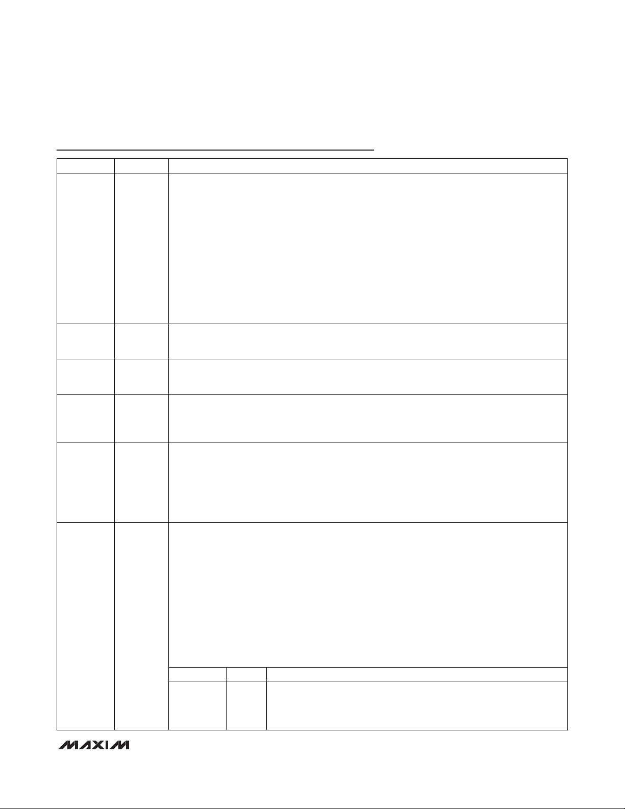
when the output voltage sensed at FB is in regulation. CLKEN is forced high in shutdown and during
soft-start and soft-stop transitions. CLKEN is forced low during dynamic VID transitions and for an
additional 20µs after the transition is completed. CLKEN is the inverse of PWRGD, except for the 5ms
PWRGD startup delay period after CLKEN is pulled low. See the startup timing diagram (Figure 9). The
CLKEN upper threshold is blanked during any downward output-voltage transition that happens when
the controller is in skip mode, and stays blanked until the slew-rate-controlled internal-transitionrelated PWRGD blanking period is complete and the output reaches regulation.
Open-Drain Power-Good Output. After output-voltage transit ions, except during power-up and powerdown, if FB is in regulation, then PWRGD is high impedance.
PWRGD is low during startup, continues to be low while the output is at the boot voltage, and stays
low until 5ms (typ) after CLKEN goes low, after which it starts monitoring the FB voltage and goes
high if FB is within the PWRGD threshold window.
PWRGD is forced low during soft-shutdown and whi le in shutdown. PWRGD is forced high
impedance whenever the slew-rate controller is active (output-voltage transitions), and continues
to be forced high impedance for an additional 20µs after the transition is completed.
The PWRGD upper threshold i s blanked during any downward output-voltage trans ition that
happens when the controller is in skip mode, and stays blanked unt il the slew-rate-controlled
internal-transit ion-related PWRGD blanking period i s complete and the output reaches regulation.
A pullup resistor on PWRGD causes additional finite shutdown current.
Driver S kip Control Output. Push/pull logic output that controls the operating mode of the skipmode driver IC. DRSKP swings from V
forced-PWM mode. When DRSKP is low, the driver ICs enable their zero-crossing comparators and
operate in pulse-s kipping mode. DRSKP goes low at the end of the soft-shutdown sequence,
instructing the external dri vers to shut down.
= 16.26pF.
TON
Very low current (1-phase sk ip)
X
Intermediate power potential (N-1-phase PWM)
0
Max power potential (full-phase PWM: N-phase or 1 phase as set by user
1
at CSP2, CSP3)
fSW = 1/(C
DD
x (R
TON
to GND. When DRSKP is high, the driver ICs operate in
+ 6.5k))
TON
IN(MIN)/RTON
. This inverted logic output indicates
3P3
] 10µA where V
IN(MIN)
is
Page 15

MAX17030/MAX17036
1/2/3-Phase Quick-PWM
IMVP-6.5 VID Controllers
______________________________________________________________________________________ 15
Pin Description (continued)
PIN NAME FUNCTION
20 PWM3
21 BST2
22 LX2
23 DH2 Phase 2 High-Side Gate-Driver Output. DH2 swings from LX2 to BST2. Low in shutdown.
24 DL2
25 VRHOT
26 V
27 DL1
28 DH1 Phase 1 High-Side Gate-Driver Output. DH1 swings from LX1 to BST1. Low in shutdown.
29 LX1
30 BST1
31 PGD _IN
32–38 D0–D6
39 CSP1
DD
PWM Signal Output for Phase 3. Swings from GND to V
(in shutdown, when CSP3 is connected to V
Phase 2 Boost Flying Capacitor Connection. BST2 is the internal upper supply rail for the DH2 highside gate driver. An internal switch between VDD and BST2 charges the BST2-LX2 flying capacitor
while the low-side MOSFET is on (DL2 pulled high).
Phase 2 Inductor Connection. LX2 is the internal lower supply rail for the DH2 high-side gate driver.
Also used as an input to phase 2’s zero-crossing comparator.
Phase 2 Low-Side Gate-Driver Output. DL2 sw ings from GND to VDD. DL2 is f orced low in shutdown.
DL2 i s forced high when an output o vervoltage fault i s detected, overriding any negati ve currentlimit condition that might be present. DL2 is forced low in skip mode after detecting an inductor
current zero cross ing.
Open-Drain Output of Internal Comparator. VRHOT is pulled low when the voltage at THRM goes
below 1.5V (30% of V
Supply Voltage Input for the DL_ Drivers. VDD is also the supply voltage used to internally recharge
the BST _-LX_ fly ing capacitor during the time s the respectiv e DL_s are high. Connect VDD to the
4.5V to 5.5V s ystem supply vo ltage. Bypass VDD to GND with a 1µF or greater ceramic capacitor.
Phase 1 Low-Side Gate-Driver Output. DL1 sw ings from GND to VDD. DL1 is f orced low in shutdown.
DL1 i s forced high when an output o vervoltage fault i s detected, overriding any negati ve currentlimit condition that might be present. DL1 is forced low in skip mode after detecting an inductor
current zero crossing.
Phase 1 Inductor Connection. LX1 is the internal lower supply rail for the DH1 high-side gate driver.
Also used as an input to phase 1’s zero-crossing comparator.
Phase 1 Boost Flying Capacitor Connection. BST1 is the internal upper supply rail for the DH1 highside gate driver. An internal switch between VDD and BST1 charges the BST1-LX1 flying capacitor
while the low-side MOSFET is on (DL1 pulled high).
Power-Good Logic Input Pin that Indicates the Power Status of Other System Rails and Used for Supply
Sequencing. During startup, after soft-starting to the boot voltage, the output voltage remains at V
and the CLKEN and PWRGD outputs remain high and low, respectively, as long as the PGD_IN input
stays low. When PGD_IN later goes high, the output is allowed to transition to the voltage set by the VID
code, and CLKEN is allowed to go low. During normal operation, if PGD_IN goes low, the controller
immediately forces CLKEN high and PWRGD low, and slews the output to the boot voltage while in skip
mode at 1/4 the normal slew rate set by the TIME resistor. The output then stays at the boot voltage until
the controller is turned off or power cycled, or until PGD_IN goes high again.
Low-Voltage (1.0V Logic) VID DAC Code Inputs. The D0–D6 inputs do not have internal pullups. These
1.0V logic inputs are designed to interface directly with the CPU. The output voltage is set by the VID
code indicated by the logic-level voltages on D0–D6 (see Table 4).
The 1111111 code corresponds to a shutdown mode. When this code is detected, The
MAX17030/MAX17036 initiate a soft-shutdown transition identical to the shutdown transition for a
SHDN fall ing edge. After slewing the output to 0V, it forces DH_, DL_, and DRSKP low, and three-states
PWM3. The IC remains active and its VCC quiescent current consumption stays the same as in normal
operation. If D6–D0 is changed from 1111111 to a different code, the MAX17030/MAX17036 initiate a
startup sequence identical to the startup sequence for a SHDN rising edge.
Positive Input of the Output Current Sense of Phase 1. This pin should be connected to the positive
side of the output current-sensing resistor or the filtering capacitor if the DC resistance of the output
inductor is util ized for current sensing.
). VRHOT is high impedance in shutdown.
CC
, and when operating with fewer than al l phases).
CC
. Three-state whenever phase 3 is disabled
DD
BOOT
,
Page 16

MAX17030/MAX17036
1/2/3-Phase Quick-PWM
IMVP-6.5 VID Controllers
16 ______________________________________________________________________________________
Pin Description (continued)
Figure 1. Standard 3-Phase IMVP-6.5 Application Circuit
PIN NAME FUNCTION
Negative Input of the Output Current Sense of Phase 1. This pin should be connected to the
40 CSN1
— PAD (GND)
VID INPUTS
ON OFF (VRON)
V
CCP
V
DPRSLPVR
5V BIAS
R
VRHOT
56Ω
SS_SENSE
V
CC
PGDIN
3.3V
PSI
R
20Ω
C
VCC
1.0µF
R
VCC
CLKEN
1.9kΩ
2.2µF
R
ILIM1RILIM2
R
R
THRM
13kΩ
100kΩ
β = 4250
negative side of the output current-sensing resistor or the filtering capacitor if the DC resistance of
the output inductor is utilized for current sensing. A 10 discharge FET is turned on in UVLO event
or thermal shutdown, or at the end of soft-shutdown.
Exposed Backplate (Pad) of Package. Internally connected to both analog ground and power
(driver) grounds. Connect to the ground plane through a thermally enhanced via.
200kΩ
TON
BST1
DH1
LX1
DL1
CSP1
CSN1
BST2
DH2
LX2
DL2
CSP2
CSN2
PWM3
DRSKP
CSP3
CSN3
FBAC
GNDS
16
30
28
C
BST
29
27
39
C
40
21
23
C
BST
22
24
12
C
11
20
19
2
C
1
9
8
FB
10
C
VDD
PWRGD
1.9kΩ
R
IMON
NTC
32
33
34
35
36
37
38
13
14
31
15
26
7
5
6
18
25
17
4
3
D0
D1
D2
D3
D4
D5
D6
SHDN
DPRSLPVR
PGDIN
PSI
V
DD
MAX17030
V
MAX17036
CC
ILIM
TIME
PWRGD
VRHOT
CLKEN
IMONIMON
THRM
PAD
R
2Ω
2Ω
CS3
TON
2Ω
CS1
CS2
C
VCC1
1.0µF
8V TO 20V
PWR INPUT
C
R3
R
NTC1
8V TO 20V
PWR INPUT
R6
R
NTC2
C
BST
IN
N
L
R
CATCHGND
10Ω
V
CC_SENSE
V
SS_SENSE
OUTPUT
(IMVP-6.5 CORE)
C
OUT
C
OUT
8V TO 20V
PWR INPUT
C
IN
N
H
L3
R7
R8
CPU REMOTE
SENSE
R9
R
NTC3
R
CATCHCORE
10Ω
C
OUT
N
H
N
L
N
H
N
L
5V BIAS
V
CC
MAX8791
PWM
SKIP
R
FB
C
FBS
1000pF
C
GNDS
4700pF
L1
R1
R2
C
IN
L2
R4
R5
BST
DH
LX
DL
GND
R
FBS
10Ω
R
GNDS
10Ω
Page 17

MAX17030/MAX17036
1/2/3-Phase Quick-PWM
IMVP-6.5 VID Controllers
______________________________________________________________________________________ 17
Table 1. Component Selection for Standard Applications
DESIGN PARAMETERS
Circuit Figure 1 Figure 1 Figure 2
Input Voltage Range 8V to 20V 8V to 20V 8V to 20V
Max imum Load Current 65A (48A TDC) 52A (38A TDC) 52A (38A TDC)
Transient Load Current
Load Line -1.9mV/A -1.9mV/A -1.9mV/A
POC Setting 110 101 101
TON Resistance (R
Inductance (L)
High-Side MOSFET (NH)
Low-Side MOSFET (NL)
Output Capacitors (C
(MAX17030 Only)
Contact Maxim for MAX17036
reference design
Input Capacitors (CIN) 6x 10µF 25V ceramic (1210) 4x 10µF 25V ceram ic (1210) 4x 10µF 25V ceramic (1210)
TIME-ILIM Resistance (R
ILIM-GND Resistance (R
FB Resistance (RFB) 6.04 k 453 k 6.04 k
IMON Resistance (R
LX-CSP Res is tance 2.21k (R1, R4, R7) 1.4k (R1, R4, R7) 2.21k (R1, R7)
CSP-CSN Resistance
DCR Sense NTC (R
DCR Sense Capacitance
SENSE
)
(C
) 200k (fSW = 300kHz) 200 k (fSW = 300kHz) 200 k (fSW = 300kHz)
TON
)
OUT
) 14k 14k 16.9k
ILIM2
) 137k 137k 133k
ILIM1
) 12.1k 10.2 k 14k
IMON
)
NTC
IMVP-6.5 XE CORE
3-PHASE
49A
(100A/µ s)
0.36µH, 36A, 0.82m
(10mm x 10mm)
Panasonic ETQP4LR36ZFC
Fairch ildsem i
1x FDS6298
9.4m/12m (typ/max)
Toshiba
1x TPCA8030-H
9.6m/13.4m (typ/max)
Fairch ildsem i
2x FDS8670
4.2m/5m (typ/max)
Toshiba
2x TPCA8019-H
4x 330µF, 2V, 4.5m
Panasonic EEFSXOD331E4 or
NEC/Tok in PSGVOE337M4.5
27x 22µF, 6.3V X5R
ceramic capacitor (0805)
3.24k (R2, R5, R8)
40.2k (R3, R6, R9)
10k NTC B = 3380
TDK NTCG163JH103F
0.22µF, 6V ceram ic (0805) 0.22µF, 6V ceramic (0805) 0.22µF, 6V ceramic (0805)
IMVP-6.5 SV CORE
3-PHASE
39A
(100A/µ s)
0.42µH, 20A, 1.55m
(7mm x 7mm)
NEC/TOKIN MPC0740LR42C
Fairch ildsem i
1x FDS6298
9.4m/12m (typ/max)
Toshiba
1x TPCA8030-H
9.6m/13.4m (typ/max
Fairch ildsem i
1x FDS8670
4.2m/5m (typ/max)
Toshiba
1x TPCA8019-H
3x 330µF, 2V, 4.5m
Panasonic EEFSXOD331E4 or
NEC/Tok in PSGVOE337M4.5
27x 22µF, 6.3V X5R
ceramic capacitor (0805)
2k (R2, R5, R8)
40.2k (R3, R6, R9)
10k NTC B = 3380
TDK NTCG163JH103F
IMVP-6.5 SV CORE
2-PHASE
39A
(100A/µ s)
0.36µH, 36A, 0.82m
(10mm x 10mm)
Panasonic ETQP4LR36ZFC
Fairch ildsem i
1x FDS6298
9.4m/12m (typ/max)
Toshiba
1x TPCA8030-H
9.6m/13.4m (typ/max)
Fairch ildsem i
2x FDS8670
4.2m/5m (typ/max)
Toshiba
2x TPCA8019-H
4x 330µF, 6m, 2.5V
Panasonic EEFSX0D0D331XR
28x 10µF, 6V ceramic (0805)
3.24k (R2, R8)
40.2k (R3, R9)
10k NTC B = 3380
TDK NTCG163JH103F
Page 18

MAX17030/MAX17036
1/2/3-Phase Quick-PWM
IMVP-6.5 VID Controllers
18 ______________________________________________________________________________________
Table 2. Component Suppliers
Figure 2. Standard 2-Phase IMVP-6.5 Application Circuit
MANUFACTURER W EBSITE
AVX Corp. www.avxcorp.com
Fairch ild Semiconductor www.fairchildsemi.com
NEC/TOKIN America, Inc. www.nec-tokinamerica.com
Panason ic Corp. www.panason ic.com
SANYO Electric Co., Ltd. www.sanyodevice.com
32
D0
33
D1
34
D2
35
VID INPUTS
ON OFF (VRON)
DPRSLPVR
5V BIAS
PGDIN
PSI
1.0µF
C
R
VCC
20Ω
C
VCC
VDD
2.2µF
R
ILIM1
R
ILIM2
36
37
38
13
14
31
15
26
7
5
6
D3
D4
D5
D6
SHDN
DPRSLPVR
PGDIN
PSI
V
DD
V
CC
MAX17030
MAX17036
ILIM
TIME
TON
BST1
DH1
LX1
DL1
CSP1
CSN1
BST2
DH2
LX2
DL2
MANUFACTURER W EBSITE
Siliconix (Visha y) www.vishay.com
Taiyo Yuden www.t-yuden.com
TDK Corp. www.component.td k.com
TOKO America, Inc. www.tokoam.com
Toshiba America Electronic
Component s, Inc.
R
TON
200kΩ
16
30
28
C
BST
29
27
39
2Ω
C
CS1
40
21
23
C
BST
22
24
N
H
N
L
N
H
N
L
L1
R1
R7
R3
R
R2
NTC1
8V TO 20V
PWR INPUT
C
IN
L2
R9
www.tosh iba.com/taec
8V TO 20V
PWR INPUT
C
IN
OUTPUT
(IMVP-6.5 CORE)
C
OUT
C
OUT
V
CCP
V
R
VRHOT
56Ω
SS_SENSE
V
3.3V
R
R
CC
CLKEN
1.9kΩ
R
THRM
13kΩ
PWRGD
1.9kΩ
R
IMON
NTC
100kΩ
β = 4250
18
PWRGD
25
VRHOT
17
CLKEN
4
IMONIMON
3
THRM
PAD
CSP2
CSN2
PWM3
DRSKP
CSP3
CSN3
FBAC
GNDS
12
2Ω
C
CS2
11
20
19
2
1
9
8
FB
10
R
FB
5V BIAS
C
FBS
1000pF
R
R8
NTC3
R
CATCHCORE
10Ω
R
CATCHGND
10Ω
V
CC_SENSE
V
SS_SENSE
R
R
10Ω
GNDS
10Ω
FBS
CPU REMOTE
SENSE
Page 19

MAX17030/MAX17036
1/2/3-Phase Quick-PWM
IMVP-6.5 VID Controllers
______________________________________________________________________________________ 19
Figure 3. Functional Diagram
THRM
VRHOT
CSP3
CSN3
CSP2
CSN2
CSP1
CSN1
ILIM
TIME
V
D0–D6
PGDIN
SHDN
PHASE 3 DRIVER
CONTROL
0.3 x V
CC
Q TRIG3
TRIG
TON
CC13
FB
MAIN PHASE
Q
S
R
LX1
0mV
ONE-SHOT
PHASE 3
ON-TIME
PHASE 2 DRIVERS
Q TRIG
ONE-SHOT
PHASE 2
ON-TIME
PHASE 1
ON-TIME
ONE-SHOT
Q TRIG
R
S
10x
10x
10x
MINIMUM
OFF-TIME
Q TRIG TRIG 3
CC
REF
(2.0V)
GND
DAC
FAULT
R-TO-I
CONVERTER
TARGET
SLEW
PHASE
SEL
ONE SHOT
PGND1
CC12
DRIVERS
Q
G
G
G
G
m(CCI)
m(CCI)
m(CCI)
m(CCI)
CSN3
CSP3
CSP1
CSN1
CSN2
CSP2
CSP1
CSN1
PWM3
DRSKP
BST2
DH2
LX2
DL2
GND
TON
BST1
DH1
LX1
V
DD
FB
GNDS
x3
FBAC
G
m(FB)
CSP
CSN
MAX17030
MAX17036
TARGET
- 300mV
SKIP
MODE/PHASE/SLEW-
RATE CONTROL
PGDIN DPRSLPVR PSI
BLANK
SKIP
TARGET
+ 200mV
CSP
CSN
5ms
STARTUP
DELAY
60µs
G
m(IMON)
DL1
GND
PWRGD
CLKEN
x3
IMON
Page 20

MAX17030/MAX17036
1/2/3-Phase Quick-PWM
IMVP-6.5 VID Controllers
20 ______________________________________________________________________________________
Detailed Description
Free-Running, Constant-On-Time PWM
Controller with Input Feed-Forward
The Quick-PWM control architecture is a pseudo-fixedfrequency, constant-on-time, current-mode regulator with
voltage feed-forward (Figure 3). This architecture relies on
the output filter capacitor’s ESR to act as the currentsense resistor, so the output ripple voltage provides the
PWM ramp signal. The control algorithm is simple: the
high-side switch on-time is determined solely by a oneshot whose period is inversely proportional to input voltage, and directly proportional to output voltage or the
difference between the main and secondary inductor currents (see the
On-Time One-Shot
section). Another oneshot sets a minimum off-time. The on-time one-shot
triggers when the error comparator goes low, the inductor
current of the selected phase is below the valley currentlimit threshold, and the minimum off-time one-shot times
out. The controller maintains 120° out-of-phase operation
by alternately triggering the three phases after the error
comparator drops below the output-voltage set point.
Triple 120° Out-of-Phase Operation
The three phases in the MAX17030/MAX17036 operate
120° out-of-phase to minimize input and output filtering
requirements, reduce electromagnetic interference (EMI),
and improve efficiency. This effectively lowers component
count—reducing cost, board space, and component
power requirements—making the MAX17030/MAX17036
ideal for high-power, cost-sensitive applications.
The MAX17030/MAX17036 share the current between
three phases that operate 120° out-of-phase, so the
high-side MOSFETs never turn on simultaneously during normal operation. The instantaneous input current
of each phase is effectively reduced, resulting in
reduced input voltage ripple, ESR power loss, and RMS
ripple current (see the
Input Capacitor Selection
section). Therefore, the same performance can be
achieved with fewer or less-expensive input capacitors.
+5V Bias Supply (VCCand VDD)
The Quick-PWM controller requires an external +5V
bias supply in addition to the battery. Typically, this
+5V bias supply is the notebook’s 95% efficient +5V
system supply. The +5V bias supply must provide V
CC
(PWM controller) and VDD(gate-drive power), so the
maximum current drawn is:
where ICCis provided in the
Electrical Characteristics
table, fSWis the switching frequency, and Q
G(LOW)
and
Q
G(HIGH)
are the MOSFET data sheet’s total gate-
charge specification limits at VGS= 5V.
V
IN
and VDDcan be connected together if the input
power source is a fixed +4.5V to +5.5V supply. If the
+5V bias supply is powered up prior to the battery supply, the enable signal (SHDN going from low to high)
must be delayed until the battery voltage is present to
ensure startup.
Switching Frequency (TON)
Connect a resistor (R
TON
) between TON and VINto set
the switching period TSW= 1/fSW, per phase:
TSW= 16.26pF x (R
TON
+ 6.5kΩ)
A 96.75kΩ to 303.25kΩ corresponds to switching periods of 167ns (600kHz) to 500ns (200kHz), respectively.
High-frequency (600kHz) operation optimizes the application for the smallest component size, trading off efficiency due to higher switching losses. Low-frequency
(200kHz) operation offers the best overall efficiency at
the expense of component size and board space.
TON Open-Circuit Protection
The TON input includes open-circuit protection to avoid
long, uncontrolled on-times that could result in an overvoltage condition on the output. The MAX17030/
MAX17036 detect an open-circuit fault if the TON current
drops below 10µA for any reason—the TON resistor
(R
TON
) is unpopulated, a high resistance value is used,
the input voltage is low, etc. Under these conditions, the
MAX17030/MAX17036 stop switching (DH and DL pulled
low) and immediately set the fault latch. Toggle SHDN or
cycle the VCCpower supply below 0.5V to clear the fault
latch and reactivate the controller.
On-Time One-Shot
The MAX17030/MAX17036 contain a fast, low-jitter,
adjustable one-shot that sets the high-side MOSFETs
on-time. It is shared among the three phases. The oneshot for the main phase varies the on-time in response
to the input and feedback voltages. The main high-side
switch on-time is inversely proportional to the input voltage as measured by the V+ input, and proportional to
the feedback voltage (VFB):
The one-shot for the second phase and third phase
varies the on-time in response to the input voltage and
the difference between the main and the other inductor
currents. Two identical transconductance amplifiers
integrate the difference between the master and each
slave’s current-sense signals. The summed output is
connected to an internal integrator for each masterslave pair, which serves as the input to the respective
slave’s high-side MOSFET TON timer.
IIfQ Q
=+ +
BIAS CC SW G LOW G HIGH
()
() ( )
TV V
()
ON
=
SW FB
t
+
0 075.
V
IN
Page 21

MAX17030/MAX17036
1/2/3-Phase Quick-PWM
IMVP-6.5 VID Controllers
______________________________________________________________________________________ 21
When the main and other phase current-sense signals
(VCM= V
CMP
- V
CMN
and VCS= V
CSP
- V
CSM
) become
unbalanced, the transconductance amplifiers adjust the
other phase’s on-time, which increases or decreases
the phase inductor current until the current-sense signals are properly balanced:
where V
CCI
is the internal integrator node for each
slave’s current-balance integrator, and Z
CCI
is the
effective impedance at that node.
During phase overlap, tONis calculated based on
phase 1’s on-time requirements, but reduced by 33%
when operating with three phases.
For a 3-phase regulator, each phase cannot be
enabled until the other 2 phases have completed their
on-time and the minimum off-times have expired. As
such, the minimum period is limited by 3 x (tON+
t
OFF(MIN)
). Maximum tONis dependent on minimum V
IN
and maximum output voltage:
T
SW(MIN)
= NPHx (t
ON(MAX)
+ t
OFF(MIN)
)
where:
t
ON(MAX)
= V
FB(MAX)/VIN(MIN
x T
SW(MIN)
so:
T
SW(MIN)
= t
OFF(MIN)
/[1/NPH– V
IN(MAX)/VIN(MIN)
]
Hence, for a 7V input and 1.1V output, 500kHz is the
maximum switching frequency. Running at this limit is
not desirable as there is no room to allow the regulator
to make adjustments without triggering phase overlap.
For a 3-phase, high-current application with minimum
8V input, the practical switching frequency is 300kHz.
On-times translate only roughly to switching frequencies. The on-times guaranteed in the
Electrical
Characteristics
are influenced by parasitics in the conduction paths and propagation delays. For loads above
the critical conduction point, where the dead-time effect
(LX flying high and conducting through the high-side
FET body diode) is no longer a factor, the actual
switching frequency (per phase) is:
where V
DIS
and V
CHG
are the sum of the parasitic volt-
age drops in the inductor discharge and charge paths,
including MOSFET, inductor, and PCB resistances;
V
CHG
is the sum of the parasitic voltage drops in the
inductor charge path, including high-side switch,
inductor, and PCB resistances; and tONis the on-time
as determined above.
Current Sense
The MAX17030/MAX17036 sense the output current of
each phase allowing the use of current-sense resistors
on inductor DCR as the current-sense element. Lowoffset amplifiers are used for current balance, voltagepositioning gain, and current limit.
Using the DC resistance (R
DCR
) of the output inductor
allows higher efficiency. The initial tolerance and temperature coefficient of the inductor’s DCR must be
accounted for in the output-voltage droop-error budget
and current monitor. This current-sense method uses
an RC filtering network to extract the current information
from the output inductor (see Figure 4). The RC network
should match the inductor’s time constant (L/R
DCR
):
and:
where RCSis the required current-sense resistance,
and R
DCR
is the inductor’s series DC resistance. Use
the typical inductance and R
DCR
values provided by
the inductor manufacturer. To minimize the currentsense error due to the current-sense inputs’ bias current
(I
CSP_
and I
CSN_
), choose R1//R2 to be less than 2kΩ
and use the above equation to determine the sense
capacitance (CEQ). Choose capacitors with 5% tolerance and resistors with 1% tolerance specifications.
Temperature compensation is recommended for this
current-sense method. See the
Voltage Positioning and
Loop Compensation
section for detailed information.
When using a current-sense resistor for accurate output-voltage positioning, the circuit requires a differential
RC filter to eliminate the AC voltage step caused by the
equivalent series inductance (L
ESL
) of the currentsense resistor (see Figure 4). The ESL induced voltage
step might affect the average current-sense voltage.
The RC filter’s time constant should match the L
ESL
/
R
SENSE
time constant formed by the current-sense
resistor’s parasitic inductance:
⎛
VV
+
tT
=
ON SEC SW
()
=
= Main O n-ttime Secondary Current Balance Correctio
CCI
⎜
V
⎝
⎛
V
+
FB
T
SW
⎜
V
⎝
()
⎞
.
0 075
⎟
⎠
IN
⎞
⎛
775V
.
00
⎟
⎠
IN
+ nn
()
IZ
T
+
SW
⎜
⎝
CCI CCI
V
IN
⎞
⎟
⎠
VV
+
()
OUT DIS
tVV V
ON IN DIS CHG
+−
()
f
SW
=
⎛
R
=
⎜
CS DCR
⎝
R
=+
CS
CRR
L
ESL
R
SENSE
2
R
⎞
R
⎟
⎠
+
12
RR
L
111
EQ
⎡
⎢
⎣
⎤
⎥
2
⎦
=
CR
EQ EQ
Page 22

MAX17030/MAX17036
1/2/3-Phase Quick-PWM
IMVP-6.5 VID Controllers
22 ______________________________________________________________________________________
where L
ESL
is the equivalent series inductance of the cur-
rent-sense resistor, R
SENSE
is current-sense resistance
value, and CEQand REQare the time-constant matching
components.
Current Balance
The MAX17030/MAX17036 integrate the difference
between the current-sense voltages and adjust the ontime of the secondary phase to maintain current balance. The current balance relies on the accuracy of the
current-sense signals across the current-sense resistor
or inductor DCR. With active current balancing, the current mismatch is determined by the current-sense resistor or inductor DCR values and the offset voltage of the
transconductance amplifiers:
where R
SENSE
= RCM= RCSand V
OS(IBAL)
is the
current balance offset specification in the
Electrical
Characteristics
table.
The worst-case current mismatch occurs immediately
after a load transient due to inductor value mismatches
resulting in different di/dt for the two phases. The time it
takes the current-balance loop to correct the transient
imbalance depends on the mismatch between the
inductor values and switching frequency.
Figure 4. Current-Sense Methods
C
IN
N
DH_
LX_
H
L
INPUT (V
IN
SENSE RESISTOR
L
ESL
)
R
SENSE
MAX17030
MAX17036
A) OUTPUT SERIES RESISTOR SENSING
MAX17030
MAX17036
B) LOSSLESS INDUCTOR SENSING
DL_
CSP_
CSN_
DH_
LX_
DL_
CSP_
CSN_
N
L
N
H
N
L
R2
R1 + R2
L
R1 R2C
[ + ]
EQ
R
R
L
ESL
SENSE
DCR
11
C
D
L
R
EQ
INPUT (V
C
IN
INDUCTOR
R
L
D
L
R1
DCR
R2
C
EQ
FOR THERMAL COMPENSATION:
R2 SHOULD CONSIST OF AN NTC RESISTOR IN
SERIES WITH A STANDARD THIN-FILM RESISTOR
C
EQ
)
IN
C
OUT
OUT
R
R
DCR
CS
CEQREQ =
=
=
III
OS IBAL LMAIN LSEC
=−=
()
V
OS IBAL
()
R
SENSE
Page 23

MAX17030/MAX17036
1/2/3-Phase Quick-PWM
IMVP-6.5 VID Controllers
______________________________________________________________________________________ 23
Current Limit
The current-limit circuit employs a unique “valley” current-sensing algorithm that senses the voltage across
the current-sense resistors or inductor DCR at the current-sense inputs (CSP_ to CSN_). If the current-sense
signal of the selected phase is above the current-limit
threshold, the PWM controller does not initiate a new
cycle until the inductor current of the selected phase
drops below the valley current-limit threshold. When
any one phase exceeds the current limit, all phases are
effectively current limited since the interleaved controller does not initiate a cycle with the next phase.
Since only the valley current is actively limited, the actual peak current is greater than the current-limit threshold by an amount equal to the inductor ripple current.
Therefore, the exact current-limit characteristic and
maximum load capability are a function of the currentsense resistance, inductor value, and battery voltage.
The positive valley current-limit threshold voltage at
CSP to CSN equals precisely 1/10 of the differential
TIME to ILIM voltage over a 0.1V to 0.5V range (10mV
to 50mV current-sense range). Connect ILIM directly to
V
CC
to set the default current-limit threshold setting of
22.5mV (typ).
The negative current-limit threshold (forced-PWM mode
only) is nominally -125% of the corresponding valley
current-limit threshold. When the inductor current drops
below the negative current limit, the controller immediately activates an on-time pulse—DL turns off, and DH
turns on—allowing the inductor current to remain above
the negative current threshold.
Carefully observe the PCB layout guidelines to ensure
that noise and DC errors do not corrupt the current-sense
signals seen by the current-sense inputs (CSP_, CSN_).
Feedback Adjustment Amplifiers
Voltage-Positioning Amplifier
(Steady-State Droop)
The MAX17030/MAX17036 include a transconductance
amplifier for adding gain to the voltage-positioning sense
path. The amplifier’s input is generated by summing the
current-sense inputs, which differentially sense the voltage across either current-sense resistors or the inductor’s DCR. The amplifier’s output connects directly to the
regulator’s voltage-positioned feedback input (FB), so
the resistance between FB and the output-voltage sense
point determines the voltage-positioning gain:
where the target voltage (V
TARGET
) is defined in the
Nominal Output Voltage Selection
section, and the FB
amplifier’s output current (I
FB
) is determined by the
sum of the current-sense voltages:
where V
CSX
= V
CSP
- V
CSN
is the differential current-
sense voltage, and G
m(FB)
is typically 400µS as
defined in the
Electrical Characteristics
.
Differential Remote Sense
The MAX17030/MAX17036 include differential, remotesense inputs to eliminate the effects of voltage drops
along the PCB traces and through the processor’s
power pins. The feedback-sense node connects to the
voltage-positioning resistor (RFB). The ground-sense
(GNDS) input connects to an amplifier that adds an offset directly to the target voltage, effectively adjusting
the output voltage to counteract the voltage drop in the
ground path. Connect the voltage-positioning resistor
(RFB) and ground sense (GNDS) input directly to the
processor’s remote sense outputs as shown in Figure 1.
Integrator Amplifier
An internal integrator amplifier forces the DC average of
the FB voltage to equal the target voltage, allowing
accurate DC output-voltage regulation regardless of the
output ripple voltage.
The MAX17030/MAX17036 disable the integrator by
connecting the amplifier inputs together at the beginning of all VID transitions done in pulse-skipping mode
(DPRSLPVR = high). The integrator remains disabled
until 20µs after the transition is completed (the internal
target settles) and the output is in regulation (edge
detected on the error comparator).
Transient Overlap Operation
When a transient occurs, the response time of the controller depends on how quickly it can slew the inductor
current. Multiphase controllers that remain 120° out-of-
phase when a transient occurs actually respond slower
than an equivalent single-phase controller. In order to
provide fast transient response, the MAX17030/
MAX17036 support a phase overlap mode, which
allows the triple regulators to operate in-phase when
heavy load transients are detected, effectively reducing
the response time. After any high-side MOSFET turns
off, if the output voltage does not exceed the regulation
voltage when the minimum off-time expires, the controller simultaneously turns on all high-side MOSFETs
with the same on-time during the next on-time cycle.
The phases remain overlapped until the output voltage
exceeds the regulation voltage after the minimum
VV RI
=−
OUT TARGET FB FB
IG V
=
FB m FB CSX
η
PH
∑
()
=
1
X
Page 24

MAX17030/MAX17036
1/2/3-Phase Quick-PWM
IMVP-6.5 VID Controllers
24 ______________________________________________________________________________________
*
Multiphase operation = All enabled phases active.
off-time expires. The on-time for each phase is based
on the input voltage to FB ratio (i.e., follows the master
on-time), but reduced by 33% in a 3-phase configuration, and not reduced in a 2-phase configuration. This
maximizes the total inductor current slew rate.
After the phase-overlap mode ends, the controller automatically begins with the next phase. For example, if
phase 2 provided the last on-time pulse before overlap
operation began, the controller starts switching with
phase 3 when overlap operation ends.
Nominal Output Voltage Selection
The nominal no-load output voltage (V
TARGET
) is
defined by the selected voltage reference (VID DAC)
plus the remote ground-sense adjustment (V
GNDS
) as
defined in the following equation:
where V
DAC
is the selected VID voltage. On startup, the
MAX17030/MAX17036 slew the target voltage from
ground to the preset boot voltage. Table 3 is the operating
mode truth table.
DAC Inputs (D0–D6)
The digital-to-analog converter (DAC) programs the output voltage using the D0–D6 inputs. D0–D6 are low-voltage (1.0V) logic inputs, designed to interface directly with
the CPU. Do not leave D0–D6 unconnected. Changing
D0–D6 initiates a transition to a new output-voltage level.
Change D0–D6 together, avoiding greater than 20ns
skew between bits. Otherwise, incorrect DAC readings
might cause a partial transition to the wrong voltage level
followed by the intended transition to the correct voltage
level, lengthening the overall transition time. The available
DAC codes and resulting output voltages are compatible
with the IMVP-6.5 (Table 4) specifications.
OFF Code
VID = 1111111 is defined as an OFF code. When the
OFF code is set, the MAX17030/MAX17036 go through
the same shutdown sequence as though SHDN has
been pulled low—output discharged to zero, CLKEN
high, and PWRGD low. Only the IC supply currents
remain at the operating levels rather than the shutdown
level. When exiting from the OFF code, the MAX17030/
MAX17036 go through the boot sequence, similar to the
sequence when SHDN is first pulled high.
Table 3. Operating Mode Truth Table
VVVV
TARGET FB DAC GNDS
== +
INPUTS
SHDN DPRSLPVR PSI
GND X X Disabled
Rising X X
High Low High
High Low Low
Multiphase Forced-PWM
Nominal R
(N-1)-Phase Forced-PWM
Nominal R
PHASE
OPERATION*
Multiphase Pulse
Skipping
1/4 R
Slew Rate
TIME
TIME
TIME
Slew Rate
Slew Rate
OPERATING MODE
Low-Power Shutdown Mode. DL1 and DL2 forced low, and the
controller i s disabled. The supply current drops to 1µA (max).
Startup/Boot. When SHDN is pulled high, the MAX17030/
MAX17036 begin the startup sequence. Once the REF is above
1.84V, the controller enables the PWM controller and ramps the
output voltage up to the boot voltage. See Figure 9.
Ful l Power. The no-load output voltage is determined by the se lected
VID DAC code (D0–D6, Table 4).
Intermediate Power. The no-load output voltage is determined by the
selected VID DAC code (D0–D6, Table 4). When PSI is pulled low,
the MAX17030/MAX17036 immediately disable phase 3, PWM3 is
three-state, and DRSKP is low.
Deeper Sleep Mode. The no-load output vo ltage is determined by the
selected VID DAC code (D0–D6, Table 4). When DPRSLPVR i s pulled
High High X
1-Phase Pulse Skipping
Nominal R
Slew Rate
TIME
high, the MAX17030/MAX17036 immediately enter 1-phase pulseskipping operation allowing automatic PWM/PFM switchover under
light load s. The PWRGD and CLKEN upper thresholds are blan ked.
DH2 and DL2 are pulled low, PWM3 i s three-state and DRSKP is low.
Page 25

MAX17030/MAX17036
1/2/3-Phase Quick-PWM
IMVP-6.5 VID Controllers
______________________________________________________________________________________ 25
Table 3. Operating Mode Truth Table (continued)
*
Multiphase operation = All enabled phases active.
Table 4. IMVP-6.5 Output Voltage VID DAC Codes
SHDN DPRSLPVR PSI
Fal ling X X
High X X Disabled
INPUTS
PHASE
OPERATION*
Multiphase Forced-PWM
1/4 R
Slew Rate
TIME
OPERATING MODE
Shutdown. When SHDN is pulled low, the MAX17030/MAX17036
immediately pull PWRGD low, CLKEN becomes high impedance, all
enabled phases are acti vated, and the output voltage is ramped
down to 12.5mV; then DH and DL are pulled low and CSNI discharge
FET is turned on.
Fault Mode. The fault latch ha s been set by the MAX17030/MAX17036
UVP or thermal-shutdown protect ion, or by the OVP protection. The
controller remains in fault mode until V
toggled.
power is cycled or SHDN
CC
OUTPUT
D6 D5 D4 D3 D2 D1 D0
0 0 0 0 0 0 0 1.5000 1 0 0 0 0 0 0 0.7000
0 0 0 0 0 0 1 1.4875 1 0 0 0 0 0 1 0.6875
0 0 0 0 0 1 0 1.4750 1 0 0 0 0 1 0 0.6750
0 0 0 0 0 1 1 1.4625 1 0 0 0 0 1 1 0.6625
0 0 0 0 1 0 0 1.4500 1 0 0 0 1 0 0 0.6500
0 0 0 0 1 0 1 1.4375 1 0 0 0 1 0 1 0.6375
0 0 0 0 1 1 0 1.4250 1 0 0 0 1 1 0 0.6250
0 0 0 0 1 1 1 1.4125 1 0 0 0 1 1 1 0.6125
0 0 0 1 0 0 0 1.4000 1 0 0 1 0 0 0 0.6000
0 0 0 1 0 0 1 1.3875 1 0 0 1 0 0 1 0.5875
0 0 0 1 0 1 0 1.3750 1 0 0 1 0 1 0 0.5750
0 0 0 1 0 1 1 1.3625 1 0 0 1 0 1 1 0.5625
0 0 0 1 1 0 0 1.3500 1 0 0 1 1 0 0 0.5500
0 0 0 1 1 0 1 1.3375 1 0 0 1 1 0 1 0.5375
0 0 0 1 1 1 0 1.3250 1 0 0 1 1 1 0 0.5250
0 0 0 1 1 1 1 1.3125 1 0 0 1 1 1 1 0.5125
0 0 1 0 0 0 0 1.3000 1 0 1 0 0 0 0 0.5000
0 0 1 0 0 0 1 1.2875 1 0 1 0 0 0 1 0.4875
0 0 1 0 0 1 0 1.2750 1 0 1 0 0 1 0 0.4750
0 0 1 0 0 1 1 1.2625 1 0 1 0 0 1 1 0.4625
0 0 1 0 1 0 0 1.2500 1 0 1 0 1 0 0 0.4500
0 0 1 0 1 0 1 1.2375 1 0 1 0 1 0 1 0.4375
0 0 1 0 1 1 0 1.2250 1 0 1 0 1 1 0 0.4250
0 0 1 0 1 1 1 1.2125 1 0 1 0 1 1 1 0.4125
0 0 1 1 0 0 0 1.2000 1 0 1 1 0 0 0 0.4000
0 0 1 1 0 0 1 1.1875 1 0 1 1 0 0 1 0.3875
VOLTAGE
(V)
D6 D5 D4 D3 D2 D1 D0
OUTPUT
VOLTAGE
(V)
Page 26

MAX17030/MAX17036
1/2/3-Phase Quick-PWM
IMVP-6.5 VID Controllers
26 ______________________________________________________________________________________
Table 4. IMVP-6.5 Output Voltage VID DAC Codes (continued)
OUTPUT
D6 D5 D4 D3 D2 D1 D0
0 0 1 1 0 1 0 1.1750 1 0 1 1 0 1 0 0.3750
0 0 1 1 0 1 1 1.1625 1 0 1 1 0 1 1 0.3625
0 0 1 1 1 0 0 1.1500 1 0 1 1 1 0 0 0.3500
0 0 1 1 1 0 1 1.1375 1 0 1 1 1 0 1 0.3375
0 0 1 1 1 1 0 1.1250 1 0 1 1 1 1 0 0.3250
0 0 1 1 1 1 1 1.1125 1 0 1 1 1 1 1 0.3125
0 1 0 0 0 0 0 1.1000 1 1 0 0 0 0 0 0.3000
0 1 0 0 0 0 1 1.0875 1 1 0 0 0 0 1 0.2875
0 1 0 0 0 1 0 1.0750 1 1 0 0 0 1 0 0.2750
0 1 0 0 0 1 1 1.0625 1 1 0 0 0 1 1 0.2625
0 1 0 0 1 0 0 1.0500 1 1 0 0 1 0 0 0.2500
0 1 0 0 1 0 1 1.0375 1 1 0 0 1 0 1 0.2375
0 1 0 0 1 1 0 1.0250 1 1 0 0 1 1 0 0.2250
0 1 0 0 1 1 1 1.0125 1 1 0 0 1 1 1 0.2125
0 1 0 1 0 0 0 1.0000 1 1 0 1 0 0 0 0.2000
0 1 0 1 0 0 1 0.9875 1 1 0 1 0 0 1 0.1875
0 1 0 1 0 1 0 0.9750 1 1 0 1 0 1 0 0.1750
0 1 0 1 0 1 1 0.9625 1 1 0 1 0 1 1 0.1625
0 1 0 1 1 0 0 0.9500 1 1 0 1 1 0 0 0.1500
0 1 0 1 1 0 1 0.9375 1 1 0 1 1 0 1 0.1375
0 1 0 1 1 1 0 0.9250 1 1 0 1 1 1 0 0.1250
0 1 0 1 1 1 1 0.9125 1 1 0 1 1 1 1 0.1125
0 1 1 0 0 0 0 0.9000 1 1 1 0 0 0 0 0.1000
0 1 1 0 0 0 1 0.8875 1 1 1 0 0 0 1 0.0875
0 1 1 0 0 1 0 0.8750 1 1 1 0 0 1 0 0.0750
0 1 1 0 0 1 1 0.8625 1 1 1 0 0 1 1 0.0625
0 1 1 0 1 0 0 0.8500 1 1 1 0 1 0 0 0.0500
0 1 1 0 1 0 1 0.8375 1 1 1 0 1 0 1 0.0375
0 1 1 0 1 1 0 0.8250 1 1 1 0 1 1 0 0.0250
0 1 1 0 1 1 1 0.8125 1 1 1 0 1 1 1 0.0125
0 1 1 1 0 0 0 0.8000 1 1 1 1 0 0 0 0
0 1 1 1 0 0 1 0.7875 1 1 1 1 0 0 1 0
0 1 1 1 0 1 0 0.7750 1 1 1 1 0 1 0 0
0 1 1 1 0 1 1 0.7625 1 1 1 1 0 1 1 0
0 1 1 1 1 0 0 0.7500 1 1 1 1 1 0 0 0
0 1 1 1 1 0 1 0.7375 1 1 1 1 1 0 1 0
0 1 1 1 1 1 0 0.7250 1 1 1 1 1 1 0 0
0 1 1 1 1 1 1 0.7125 1 1 1 1 1 1 1 Off
VOLTAGE
(V)
D6 D5 D4 D3 D2 D1 D0
OUTPUT
VOLTAGE
(V)
Page 27

MAX17030/MAX17036
1/2/3-Phase Quick-PWM
IMVP-6.5 VID Controllers
______________________________________________________________________________________ 27
Suspend Mode
When the processor enters low-power deeper sleep
mode, the IMVP-6.5 CPU sets the VID DAC code to a
lower output voltage and drives DPRSLPVR high. The
MAX17030/MAX17036 respond by slewing the internal
target voltage to the new DAC code, switching to singlephase operation, and letting the output voltage gradually drift down to the deeper sleep voltage. During the
transition, the MAX17030/MAX17036 blank both the
upper and lower PWRGD and CLKEN thresholds until
20µs after the internal target reaches the deeper sleep
voltage. Once the 20µs timer expires, the MAX17030/
MAX17036 reenable the lower PWRGD and CLKEN
threshold, but keep the upper threshold blanked.
Output-Voltage-Transition Timing
At the beginning of an output-voltage transition, the
MAX17030/MAX17036 blank both PWRGD thresholds,
preventing the PWRGD open-drain output from changing states during the transition. The controller enables
the lower PWRGD threshold approximately 20µs after
the slew-rate controller reaches the target output voltage, but the upper PWRGD threshold is enabled only if
the controller remains in forced-PWM operation. If the
controller enters pulse-skipping operation, the upper
PWRGD threshold remains blanked. The slew rate (set
by resistor R
TIME
) must be set fast enough to ensure
that the transition can be completed within the maximum allotted time.
The MAX17030/MAX17036 automatically control the current to the minimum level required to complete the transition. The total transition time depends on R
TIME
, the
voltage difference, and the accuracy of the slew-rate
controller (C
SLEW
accuracy). The slew rate is not dependent on the total output capacitance, as long as the
surge current is less than the current limit. For all dynamic VID transitions, the transition time (t
TRAN
) is given by:
where dV
TARGET
/dt = 12.5mV/µs × 71.5kΩ/R
TIME
is the
slew rate, V
OLD
is the original output voltage, and V
NEW
is the new target voltage. See TIME Slew-Rate
Accuracy in the
Electrical Characteristics
for slew-rate
limits. For soft-start and shutdown, the controller automatically reduces the slew rate to 1/4.
The average inductor current per phase required to
make an output-voltage transition is:
where dV
TARGET
/dt is the required slew rate, C
OUT
is
the total output capacitance, and η
TOTAL
is the number
of active phases.
Deeper Sleep Transitions
When DPRSLPVR goes high, the MAX17030/MAX17036
immediately disable phases 2 and 3 (DH2, DL2 forced
low, PWM3 three-state, DRSKP low), and enter pulseskipping operation (see Figures 5 and 6). If the VIDs are
set to a lower voltage setting, the output drops at a rate
determined by the load and the output capacitance. The
internal target still ramps as before, and PWRGD
remains blanked high impedance until 20µs after the
output voltage reaches the internal target. Once this
time expires, PWRGD monitors only the lower threshold:
• Fast C4E Deeper Sleep Exit: When exiting deeper
sleep (DPRSLPVR pulled low) while the output voltage still exceeds the deeper sleep voltage, the
MAX17030/MAX17036 quickly slew (50mV/µs min
regardless of R
TIME
setting) the internal target voltage to the DAC code provided by the processor as
long as the output voltage is above the new target.
The controller remains in skip mode until the output
voltage equals the internal target. Once the internal
target reaches the output voltage, phase 2 is
enabled. The controller blanks PWRGD and CLKEN
(forced high impedance) until 20µs after the transition is completed. See Figure 5.
• Standard C4 Deeper Sleep Exit: When exiting
deeper sleep (DPRSLPVR pulled low) while the output voltage is regulating to the deeper sleep voltage, the MAX17030/MAX17036 immediately
activate all enabled phases and ramp the output
voltage to the LFM DAC code provided by the
processor at the slew rate set by R
TIME
. The con-
troller blanks PWRGD and CLKEN (forced high
impedance) until 20µs after the transition is completed. See Figure 6.
VV
t
TRAN
NEW OLD
=
dV dt
()
TARGET
−
C
I
OUT
≅×
L
η
TOTAL
dV dt
()
TARGET
Page 28
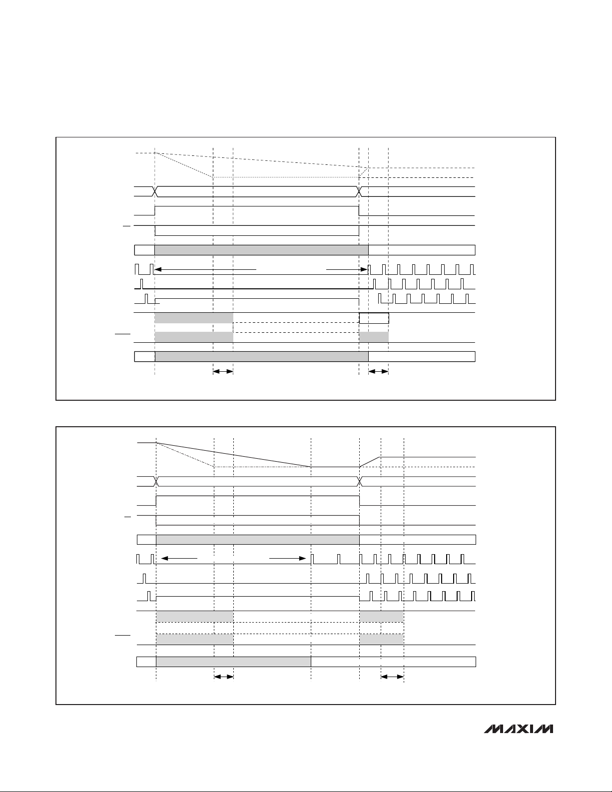
MAX17030/MAX17036
1/2/3-Phase Quick-PWM
IMVP-6.5 VID Controllers
28 ______________________________________________________________________________________
Figure 5. C4E (C4 Early Exit) Transition
DPRSLPVR
INTERNAL
PWM CONTROL
DH1
OVP
CPU CORE
VOLTAGE
INTERNAL
TARGET
ACTUAL V
OUT
PSI
VID (D0–D6)
ACTIVE VID
LFM VID
DPRSLP VID
DH2
PWM3
t
BLANK
20µs TYP
t
BLANK
20µs TYP
SET TO 1.5V MIN TRACKS INTERNAL TARGET
NO PULSES: V
OUT
> V
TARGET
1-PHASE SKIP (DH1 ACTIVE, DH2, DL2 FORCED LOW, PWM3 THREE-STATE)
DO NOT CARE (DPRSLPVR DOMINATES STATE)
FORCED-PWM
DEEPER SLEEP VID
LFM VID
PWRGD
CLKEN
BLANK LOW
BLANK HIGH THRESHOLD ONLY
BLANK HIGH THRESHOLD ONLY
BLANK HIGH-Z
BLANK LOW
BLANK HIGH-Z
Figure 6. Standard C4 Transition
ACTUAL V
CPU CORE
VOLTAGE
INTERNAL TARGET
OUT
VID (D0–D6)
DPRSLPVR
PSI
INTERNAL
PWM CONTROL
DH1
DH2
PWM3
PWRGD
CLKEN
OVP
1-PHASE SKIP (DH1 ACTIVE, DH2, DL2 FORCED LOW, PWM3 THREE-STATE)
DO NOT CARE (DPRSLPVR DOMINATES STATE)
NO PULSES: V
BLANK HIGH-Z
BLANK LOW BLANK LOBLANK HIGH THRESHOLD ONLY
SET TO 1.5V MIN TRACKS INTERNAL TARGET
t
BLANK
20µs typ
DEEPER SLEEP VID
> V
OUT
TARGET
BLANK HI-ZBLANK HIGH THRESHOLD ONLY
t
BLANK
20µs typ
FORCED-PWM
Page 29

MAX17030/MAX17036
1/2/3-Phase Quick-PWM
IMVP-6.5 VID Controllers
______________________________________________________________________________________ 29
PSI Transitions
When PSI is pulled low, the MAX17030/MAX17036
immediately disable phase 3 (PWM3 three-state,
DRSKP forced low) and enter 2-phase PWM operation
(see Figure 7). When PSI is pulled high, the MAX17030/
MAX17036 enable phase 3.
Forced-PWM Operation (Normal Mode)
During soft-shutdown and normal operation—when the
CPU is actively running (DPRSLPVR = low, Table 5)—
the MAX17030/MAX17036 operate with the low-noise,
forced-PWM control scheme. Forced-PWM operation
disables the zero-crossing comparators of all active
phases, forcing the low-side gate-drive waveforms to
constantly be the complement of the high-side gatedrive waveforms. This keeps the switching frequency
constant and allows the inductor current to reverse
under light loads, providing fast, accurate negative output-voltage transitions by quickly discharging the output
capacitors.
Forced-PWM operation comes at a cost: the no-load
+5V bias supply current remains between 10mA to
50mA per phase, depending on the external MOSFETs
and switching frequency. To maintain high efficiency
under light-load conditions, the processor can switch
the controller to a low-power pulse-skipping control
scheme by entering suspend mode.
PSI determines how many phases are active when operating in forced-PWM mode (DPRSLPVR = low). When PSI
is pulled low, phases 1 and 2 remain active but phase 3
is disabled (PWM3 three-state, DRSKP forced low).
Light-Load Pulse-Skipping Operation
(Deeper Sleep)
During soft-start and normal operation when
DPRSLPVR is pulled high, the MAX17030/MAX17036
operate with a single-phase pulse-skipping mode. The
pulse-skipping mode enables the driver’s zero-crossing
comparator, so the controller pulls DL1 low when its current-sense inputs detect “zero” inductor current. This
keeps the inductor from discharging the output capacitors and forces the controller to skip pulses under lightload conditions to avoid overcharging the output.
CPU FREQ
CPU LOAD
CPU CORE
VOLTAGE
VID (D0–D6)
PWRGD
PWM3
DH2
DH1
PSI
CLKEN
t
BLANK
20µs typ
t
BLANK
20µs typ
BLANK HIGH-Z
PWM3 THREE-STATE
180° OUT-OF-PHASE
BLANK LOW
BLANK HIGH-Z
BLANK LOW
Figure 7. PSI Transition
Page 30

MAX17030/MAX17036
1/2/3-Phase Quick-PWM
IMVP-6.5 VID Controllers
30 ______________________________________________________________________________________
When pulse-skipping, the controller blanks the upper
PWRGD and CLKEN thresholds. Upon entering pulseskipping operation, the controller temporarily sets the
OVP threshold to 1.5V, preventing false OVP faults
when the transition to pulse-skipping operation coincides with a VID code change. Once the error amplifier
detects that the output voltage is in regulation, the OVP
threshold tracks the selected VID DAC code. The
MAX17030/MAX17036 automatically use forced-PWM
operation during soft-start and soft shutdown, regardless of the DPRSLPVR and PSI configuration.
Automatic Pulse-Skipping Switchover
In skip mode (DPRSLPVR = high), an inherent automatic
switchover to PFM takes place at light loads (Figure 8).
This switchover is affected by a comparator that truncates the low-side switch on-time at the inductor current’s zero crossing. The zero-crossing comparator
senses the inductor current across the low-side
MOSFETs. Once VLXdrops below the zero-crossing
comparator threshold (see the
Electrical Characteristics
),
the comparator forces DL low. This mechanism causes
the threshold between pulse-skipping PFM and nonskipping PWM operation to coincide with the boundary
between continuous and discontinuous inductor-current
operation. The PFM/PWM crossover occurs when the
load current of each phase is equal to 1/2 the peak-topeak ripple current, which is a function of the inductor
value (Figure 8). For a battery input range of 7V to 20V,
this threshold is relatively constant, with only a minor
dependence on the input voltage due to the typically
low duty cycles. The total load-current at the PFM/PWM
crossover threshold (I
LOAD(SKIP)
) is approximately:
Power-Up Sequence (POR, UVLO)
The MAX17030/MAX17036 are enabled when SHDN is
driven high (Figure 9). The reference powers up first.
Once the reference exceeds its undervoltage-lockout
(UVLO) threshold, the internal analog blocks are turned
on and masked by a 150µs one-shot delay. The PWM
controller then begins switching.
Figure 8. Pulse-Skipping/Discontinuous Crossover Point
Figure 9. Power-Up and Shutdown Sequence Timing Diagram
I
LOAD SKIP
()
TVLVV
⎛
SW OUT IN O UT
=
⎜
⎝
⎛
-
⎞
⎟
⎜
⎠
×
2
⎝
V
=
ON-TIME
– V
IN
OUT
L
TIME
∆I
∆t
INDUCTOR CURRENT
0
⎞
⎟
V
⎠⎠
IN
I
PEAK
I
= I
LOAD
/2
PEAK
V
CC
SHDN
VID (D0–D6)
1/4 SLEW RATE SET
V
CORE
INTERNAL
PWM CONTROL
CLKEN
IMVPOK
SOFT-START
BY R
TIME
IGNORE
VID
PULSE-SKIPPING
t
BLANK
60µs TYP
t
BLANK
20µs TYP
t
BLANK
5ms TYP
FORCED-PWM
t
BLANK
20µs TYP
IGNORE
VID
SOFT-SHUTDOWN
1/4 SLEW RATE SET
BY R
TIME
Page 31

MAX17030/MAX17036
1/2/3-Phase Quick-PWM
IMVP-6.5 VID Controllers
______________________________________________________________________________________ 31
Power-on reset (POR) occurs when VCCrises above
approximately 2V, resetting the fault latch and preparing the controller for operation. The VCCUVLO circuitry
inhibits switching until VCCrises above 4.25V. The controller powers up the reference once the system
enables the controller, V
CC
is above 4.25V, and SHDN
driven high. With the reference in regulation, the controller ramps the output voltage to the boot voltage
(1.1V) at 1/4 the slew rate set by R
TIME
:
where dV
TARGET
/dt = 12.5mV/µs x 71.5kΩ/R
TIME
is the
slew rate. The soft-start circuitry does not use a variable
current limit, so full output current is available immediately. CLKEN is pulled low approximately 60µs after the
MAX17030/MAX17036 reach the boot voltage. At the
same time, the MAX17030/MAX17036 slew the output
to the voltage set at the VID inputs at the programmed
slew rate. PWRGD becomes high impedance approximately 5ms after CLKEN is pulled low. The MAX17030/
MAX17036 automatically operate in pulse-skipping
mode during soft-start, and use forced-PWM operation
during soft-shutdown, regardless of the DPRSLPVR and
PSI configuration.
If the VCCvoltage drops below 4.25V, the controller
assumes that there is not enough supply voltage to make
valid decisions, and shuts down immediately. DH and DL
are forced low, and CSNI 10Ω discharge FET is enabled.
Shutdown
When SHDN goes low, the MAX17030/MAX17036
enters low-power shutdown mode. PWRGD is pulled
low immediately, and the output voltage ramps down at
1/4 the slew rate set by R
TIME
:
where dV
TARGET
/dt = 12.5mV/µs x 71.5kΩ/R
TIME
is the
slew rate. After the output voltage drops to 12.5mV, the
MAX17030/MAX17036 shut down completely—the drivers are disabled (DL1 and DL2 driven low, PWM3 is
three-state, and DRSKP low), the reference turns off,
10Ω CSNI discharge FET is turned on, and the supply
current drops below 1µA.
When an undervoltage fault condition activates the shutdown sequence, the protection circuitry sets the fault
latch to prevent the controller from restarting. To clear
the fault latch and reactivate the controller, toggle SHDN
or cycle V
CC
power below 0.5V.
Current Monitor (IMON)
The MAX17030/MAX17036 include a unidirectional
transconductance amplifier that sources current proportional to the positive current-sense voltage. The
IMON output current is defined by:
I
IMON
= G
m(IMON)
x Σ(V
CSP
- V
CSN
)
where G
m(IMON)
= 1.6mS (typ) and the IMON current is
unidirectional (sources current out of IMON only) for
positive current-sense values. For negative currentsense voltages, the IMON current is zero.
Connect an external resistor between IMON and GNDS
to create the desired IMON gain based on the following
equation:
R
IMON
= 0.9V/(I
MAX
x R
SENSE(MIN)
x G
m(IMON_MIN)
)
where I
MAX
is defined in the Current Monitor section of
the Intel IMVP-6.5 specification and based on discrete
increments (10A, 20A, 30A, 40A, etc.), R
SENSE(MIN)
is
the minimum effective value of the current-sense element (sense resistor or inductor DCR) that is used to
provide the current-sense voltage, and G
m(IMON_MIN)
is the minimum transconductance amplifier gain as
defined in the
Electrical Characteristics
.
The IMON voltage is internally clamped to a maximum
of 1.1V (typ), preventing the IMON output from exceeding the IMON voltage rating even under overload or
short-circuit conditions. When the controller is disabled,
IMON is pulled to ground.
The transconductance amplifier and voltage clamp are
internally compensated, so IMON cannot directly drive
large capacitance values. To filter the IMON signal, use
an RC filter as shown in Figure 1.
Temperature Comparator (
VRHOT
)
The MAX17030/MAX17036 also feature an independent
comparator with an accurate threshold (V
HOT
) that
tracks the analog supply voltage (V
HOT
= 0.3VCC). This
makes the thermal trip threshold independent of the V
CC
supply voltage tolerance. Use a resistor- and thermistordivider between VCCand GND to generate a voltageregulator overtemperature monitor. Place the thermistor
as close to the MOSFETs and inductors as possible.
Fault Protection (Latched)
Output Overvoltage Protection
The overvoltage-protection (OVP) circuit is designed to
protect the CPU against a shorted high-side MOSFET
by drawing high current and blowing the battery fuse.
The MAX17030/MAX17036 continuously monitor the
output for an overvoltage fault. An OVP fault is detected
if the output voltage exceeds the set VID DAC voltage
by more than 300mV, or the fixed 1.5V (typ) threshold
t
()
TRAN START
4
V
=
BOOT
dV dt
()
TARGET
t
()
TRAN SHDN
4
V
=
OUT
dV dt
()
TARGET
Page 32

MAX17030/MAX17036
1/2/3-Phase Quick-PWM
IMVP-6.5 VID Controllers
32 ______________________________________________________________________________________
during a downward VID transition in skip mode. During
pulse-skipping operation (DPRSLPVR = high), the OVP
threshold tracks the VID DAC voltage as soon as the
output is in regulation; otherwise, the fixed 1.5V (typ)
threshold is used.
When the OVP circuit detects an overvoltage fault while
in multiphase mode (DPRSLPVR = low, PSI = high), the
MAX17030/MAX17036 immediately force DL1 and DL2
high, PWM3 low, and DRSKP high; and pull DH1 and
DH2 low. This action turns on the synchronous-rectifier
MOSFETs with 100% duty and, in turn, rapidly discharges the output filter capacitor and forces the output
low. If the condition that caused the overvoltage (such
as a shorted high-side MOSFET) persists, the battery
fuse blows. Toggle SHDN or cycle the VCCpower supply
below 0.5V to clear the fault latch and reactivate the controller.
When an overvoltage fault occurs while in 1-phase
operation (DPRSLPVR = high, or PSI = low), the
MAX17030/MAX17036 immediately force DL1 high and
pull DH1 low. DL2 and DH2 remain low as phase 2 was
disabled. DL2 does not react.
Overvoltage protection can be disabled through the nofault test mode (see the
No-Fault Test Mode
section).
Output Undervoltage Protection
If the MAX17030/MAX17036 output voltage is 400mV
below the target voltage, the controller activates the
shutdown sequence and sets the fault latch. Once the
output voltage ramps down to 12.5mV, it forces the DL1
and DL2 low and pulls DH1 and DH2 low, three-states
PWM3, and sets DRSKP low 10Ω CSNI discharge FET
is turned on. Toggle SHDN or cycle the VCCpower
supply below 0.5V to clear the fault latch and reactivate
the controller.
UVP can be disabled through the no-fault test mode
(see the
No-Fault Test Mode
section).
Thermal-Fault Protection
The MAX17030/MAX17036 feature a thermal fault-protection circuit. When the junction temperature rises
above +160°C, a thermal sensor sets the fault latch and
forces the DL1 and DL2 low and pulls DH1 and DH2
low, three-states PWM3, sets DRSKP low, and enables
10Ω CSNI discharge FET on. Toggle SHDN or cycle the
VCCpower supply below 0.5V to clear the fault latch
and reactivate the controller after the junction temperature cools by 15°C.
Thermal shutdown can be disabled through the no-fault
test mode (see the
No-Fault Test Mode
section).
No-Fault Test Mode
The latched fault-protection features can complicate
the process of debugging prototype breadboards since
there are (at most) a few milliseconds in which to determine what went wrong. Therefore, a “no-fault” test
mode is provided to disable the fault protection—overvoltage protection, undervoltage protection, and thermal shutdown. Additionally, the test mode clears the
fault latch if it has been set. The no-fault test mode is
entered by forcing 11V to 13V on SHDN.
MOSFET Gate Drivers
The DH and DL drivers are optimized for driving moderate-sized high-side and larger low-side power
MOSFETs. This is consistent with the low duty factor
seen in notebook applications, where a large V
IN
-
V
OUT
differential exists. The high-side gate drivers (DH)
source 2.7A and sink 2.2A, and the low-side gate drivers (DL) source 2.7A and sink 8A. This ensures robust
gate drive for high-current applications. The DH_ floating high-side MOSFET drivers are powered by internal
boost switch charge pumps at BST_, while the DL_ synchronous-rectifier drivers are powered directly by the
5V bias supply (VDD).
Adaptive dead-time circuits monitor the DL and DH drivers and prevent either FET from turning on until the
other is fully off. The adaptive driver dead time allows
operation without shoot-through with a wide range of
MOSFETs, minimizing delays and maintaining efficiency.
A low-resistance, low-inductance path from the DL and
DH drivers to the MOSFET gates is required for the
adaptive dead-time circuits to work properly; otherwise,
the sense circuitry in the MAX17030/MAX17036 interprets the MOSFET gates as “off” while charge actually
remains. Use very short, wide traces (50 mils to 100
mils wide if the MOSFET is 1in from the driver).
The DL low on-resistance of 0.25Ω (typ) helps prevent
DL from being pulled up due to capacitive coupling from
the drain to the gate of the low-side MOSFETs when the
inductor node (LX) quickly switches from ground to VIN.
The capacitive coupling between LX and DL created by
the MOSFET’s gate-to-drain capacitance (C
RSS
), gate-
to-source capacitance (C
ISS
- C
RSS
), and additional
board parasitics should not exceed the following minimum threshold to prevent shoot-through currents:
Adding a 4700pF between DL and power ground (C
NL
in Figure 10), close to the low-side MOSFETs, greatly
reduces coupling. Do not exceed 22nF of total gate
capacitance to prevent excessive turn-off delays.
VV
GS TH IN MAX
>
() ( )
⎛
⎜
⎝
C
C
RSS
ISS
⎞
⎟
⎠
Page 33

MAX17030/MAX17036
1/2/3-Phase Quick-PWM
IMVP-6.5 VID Controllers
______________________________________________________________________________________ 33
Shoot-through currents can also be caused by a combination of fast high-side MOSFETs and slow low-side
MOSFETs. If the turn-off delay time of the low-side
MOSFET is too long, the high-side MOSFETs can turn
on before the low-side MOSFETs have actually turned
off. Adding a resistor less than 5Ω in series with BST
slows down the high-side MOSFET turn-on time, eliminating the shoot-through currents without degrading the
turn-off time (R
BST
in Figure 10). Slowing down the
high-side MOSFET also reduces the LX node rise time,
thereby reducing EMI and high-frequency coupling
responsible for switching noise.
Multiphase Quick-PWM
Design Procedure
Firmly establish the input voltage range and maximum
load current before choosing a switching frequency and
inductor operating point (ripple-current ratio). The primary design trade-off lies in choosing a good switching
frequency and inductor operating point, and the following
four factors dictate the rest of the design:
• Input voltage range: The maximum value
(V
IN(MAX)
) must accommodate the worst-case high
AC adapter voltage. The minimum value (V
IN(MIN)
)
must account for the lowest input voltage after
drops due to connectors, fuses, and battery selector switches. If there is a choice at all, lower input
voltages result in better efficiency.
• Maximum load current: There are two values to
consider. The peak load current (I
LOAD(MAX)
) determines the instantaneous component stresses and
filtering requirements, and thus drives output
capacitor selection, inductor saturation rating, and
the design of the current-limit circuit. The continuous load current (I
LOAD
) determines the thermal
stresses and thus drives the selection of input
capacitors, MOSFETs, and other critical heat-contributing components. Modern notebook CPUs generally exhibit I
LOAD
= I
LOAD(MAX)
x 80%.
For multiphase systems, each phase supports a
fraction of the load, depending on the current balancing. When properly balanced, the load current is
evenly distributed among each phase:
where
η
TOTAL
is the total number of active phases.
• Switching frequency: This choice determines the
basic trade-off between size and efficiency. The
optimal frequency is largely a function of maximum
input voltage, due to MOSFET switching losses that
are proportional to frequency and V
IN
2
. The optimum frequency is also a moving target, due to
rapid improvements in MOSFET technology that are
making higher frequencies more practical.
• Inductor operating point: This choice provides
trade-offs between size vs. efficiency and transient
response vs. output noise. Low inductor values provide better transient response and smaller physical
size, but also result in lower efficiency and higher
output noise due to increased ripple current. The
minimum practical inductor value is one that causes
the circuit to operate at the edge of critical conduction (where the inductor current just touches zero
with every cycle at maximum load). Inductor values
lower than this grant no further size-reduction benefit. The optimum operating point is usually found
between 30% and 50% ripple current. for a multiphase core regulator, select an LIR value of ~0.4.
Inductor Selection
The switching frequency and operating point (% ripple
current or LIR) determine the inductor value as follows:
where
η
TOTAL
is the total number of phases.
Figure 10. Gate Drive Circuit
(R
)*
LX_
V
BST
)
INPUT (V
IN
C
BST
C
BYP
DD
(CNL)*
N
H
L
N
L
BST_
DH_
DL_
PGND
MAX17030/MAX17036
(R
)* OPTIONAL—THE RESISTOR LOWERS EMI BY DECREASING THE
BST
SWITCHING NODE RISE TIME.
)* OPTIONAL—THE CAPACITOR REDUCES LX TO DL CAPACITIVE
(C
NL
COUPLING THAT CAN CAUSE SHOOT-THROUGH CURRENT.
I
=
LOAD
η
TOTAL
I
LOAD PHASE
()
⎛
VV
−
η
L
=
TOTAL
IN OUT
⎜
fI LIRVV
⎝
SW L OA D MA X
() IIN
⎞
⎛
⎟
⎜
⎝
⎠
⎞
OUT
⎟
⎠
Page 34

MAX17030/MAX17036
1/2/3-Phase Quick-PWM
IMVP-6.5 VID Controllers
34 ______________________________________________________________________________________
Find a low-loss inductor having the lowest possible DC
resistance that fits in the allotted dimensions. The core
must not to saturate at the peak inductor current (I
PEAK
):
Output Capacitor Selection
Output capacitor selection is determined by the controller stability requirements, and the transient soar and
sag requirements of the application.
Output Capacitor ESR
The output filter capacitor must have low enough effective series resistance (ESR) to meet output ripple and
load-transient requirements, yet have high enough ESR
to satisfy stability requirements.
In CPU V
CORE
converters and other applications where
the output is subject to large load transients, the output
capacitor’s size typically depends on how much ESR is
needed to prevent the output from dipping too low under a
load transient. Ignoring the sag due to finite capacitance:
The output ripple voltage of a step-down controller
equals the total inductor ripple current multiplied by the
output capacitor’s ESR. When operating multiphase
systems out-of-phase, the peak inductor currents of
each phase are staggered, resulting in lower output ripple voltage by reducing the total inductor ripple current.
For multiphase operation, the maximum ESR to meet
ripple requirements is:
where
η
TOTAL
is the total number of active phases and
fSWis the switching frequency per phase. The actual
capacitance value required relates to the physical size
needed to achieve low ESR, as well as to the chemistry
of the capacitor technology. Thus, the capacitor is usually selected by ESR and voltage rating rather than by
capacitance value (this is true of polymer types).
When using low-capacity ceramic filter capacitors,
capacitor size is usually determined by the capacity
needed to prevent V
SAG
and V
SOAR
from causing problems during load transients. Generally, once enough
capacitance is added to meet the overshoot requirement, undershoot at the rising load edge is no longer a
problem (see the V
SAG
and V
SOAR
equations in the
Transient Response
section).
Output Capacitor Stability Considerations
For Quick-PWM controllers, stability is determined by
the value of the ESR zero relative to the switching frequency. The boundary of instability is given by the following equation:
where:
and:
where C
OUT
is the total output capacitance, R
ESR
is the
total equivalent series resistance, R
DROOP
is the volt-
age-positioning gain, and R
PCB
is the parasitic board
resistance between the output capacitors and sense
resistors.
For a standard 300kHz application, the ESR zero frequency must be well below 95kHz, preferably below
50kHz. Tantalum, SANYO POSCAP, and Panasonic SP
capacitors in widespread use at the time of publication
have typical ESR zero frequencies below 50kHz. In the
standard application circuit, the ESR needed to support
a 30mV
P-P
ripple is 30mV/(40A x 0.3) = 2.5mΩ. Four
330µF/2.5V Panasonic SP (type SX) capacitors in parallel provide 1.5mΩ (max) ESR. With a 2mΩ droop and
0.5mΩ PCB resistance, the typical combined ESR
results in a zero at 30kHz.
Ceramic capacitors have a high ESR zero frequency, but
applications with significant voltage positioning can take
advantage of their size and low ESR. When using only
ceramic output capacitors, output overshoot (V
SOAR
)
typically determines the minimum output capacitance
requirement. Their relatively low capacitance value
favors high switching-frequency operation with small
inductor values to minimize the energy transferred from
inductor to capacitor during load-step recovery.
Unstable operation manifests itself in two related but
distinctly different ways: double-pulsing and feedback
loop instability. Double pulsing occurs due to noise on
the output or because the ESR is so low that there is not
enough voltage ramp in the output-voltage signal. This
“fools” the error comparator into triggering a new cycle
immediately after the minimum off-time period has
expired. Double pulsing is more annoying than harmful,
resulting in nothing worse than increased output ripple.
I
I
PEAK
⎛
LOAD MAX
=
⎜
⎝
η
TOTAL
⎞
⎛
()
⎜
⎟
⎝
⎠
LIR
⎞
1
+
⎟
⎠
2
R
ESR
V
RR
+
()
ESR PCB
⎡
≤
⎢
VVV
()
⎢
IN TOTAL OUT OUT
⎣
Vf L
IN SW
−
η
≤
I
∆
STEP
()
LOAD MAX
⎤
V
⎥
PPPLE
RI
⎥
⎦
f
ESR
2π
SW
≤
π
1
RC
EFF OUT
f
f
=
ESR
RRR R
=+ +
EFF ESR DROO P PCB
Page 35

MAX17030/MAX17036
1/2/3-Phase Quick-PWM
IMVP-6.5 VID Controllers
______________________________________________________________________________________ 35
However, it can indicate the possible presence of loop
instability due to insufficient ESR. Loop instability can
result in oscillations at the output after line or load
steps. Such perturbations are usually damped, but can
cause the output voltage to rise above or fall below the
tolerance limits.
The easiest method for checking stability is to apply a
very fast 10% to 90% max load transient and carefully
observe the output voltage ripple envelope for overshoot and ringing. It can help to simultaneously monitor
the inductor current with an AC current probe. Do not
allow more than one cycle of ringing after the initial
step-response under/overshoot.
Transient Response
The inductor ripple current impacts transient-response
performance, especially at low VIN- V
OUT
differentials.
Low inductor values allow the inductor current to slew
faster, replenishing charge removed from the output filter capacitors by a sudden load step. The amount of
output sag is also a function of the maximum duty factor, which can be calculated from the on-time and minimum off-time. For a dual-phase controller, the
worst-case output sag voltage can be determined by:
and:
where t
OFF(MIN)
is the minimum off-time (see the
Electrical Characteristics
), TSWis the programmed
switching period, and
η
TOTAL
is the total number of
active phases. K = 66% when NPH= 3, and K = 100%
when NPH= 2. V
SAG
must be less than the transient
droop ∆I
LOAD(MAX)
x R
DROOP
.
The capacitive soar voltage due to stored inductor
energy can be calculated as:
where
η
TOTAL
is the total number of active phases. The
actual peak of the soar voltage is dependent on the
time where the decaying ESR step and rising capacitive soar is at its maximum. This is best simulated or
measured. For the MAX17036 with transient suppression, contact Maxim directly for application support to
determine the output capacitance requirement.
Input Capacitor Selection
The input capacitor must meet the ripple current
requirement (I
RMS
) imposed by the switching currents.
The multiphase Quick-PWM controllers operate out-ofphase, reducing the RMS input. For duty cycles less
than 100%/
η
OUTPH
per phase, the I
RMS
requirements
can be determined by the following equation:
where
η
TOTAL
is the total number of out-of-phase
switching regulators. The worst-case RMS current
requirement occurs when operating with VIN=
2
η
TOTALVOUT
. At this point, the above equation simpli-
fies to I
RMS
= 0.5 x I
LOAD
/
η
TOTAL
. Choose an input
capacitor that exhibits less than +10°C temperature rise
at the RMS input current for optimal circuit longevity.
Power-MOSFET Selection
Most of the following MOSFET guidelines focus on the
challenge of obtaining high load-current capability
when using high-voltage (> 20V) AC adapters.
High-Side MOSFET Power Dissipation
The conduction loss in the high-side MOSFET (NH) is a
function of the duty factor, with the worst-case power
dissipation occurring at the minimum input voltage:
where
η
TOTAL
is the total number of phases.
Calculating the switching losses in the high-side
MOSFET (NH) is difficult since it must allow for difficult
quantifying factors that influence the turn-on and turnoff times. These factors include the internal gate resistance, gate charge, threshold voltage, source
inductance, and PCB layout characteristics. The following switching-loss calculation provides only a very
rough estimate and is no substitute for breadboard
evaluation, preferably including verification using a
thermocouple mounted on NH:
where C
OSS
is the NHMOSFET’s output capacitance,
Q
G(SW)
is the charge needed to turn on the N
H
MOSFET, and I
GATE
is the peak gate-drive source/sink
current (2.2A typ).
∆
LI
()
V
≈
SAG
LOAD(MA X)
2η
CVTKT
TOTAL OUT OUT
Ttt
=+
MIN ON O FF MIN
2
×
()
∆
IL
V
SOA R
()
≈
2η
()
LOAD MAX
CV
TOTAL OUT OUT
⎡
SSW MI N
⎣
2
MIN
T−
⎤
⎦
I
RMS
⎛
=
⎜
⎝
I
LOAD
η
TOTAL IN
⎞
ηη
⎟
V
⎠
VV
TOTAL OUT IN TOT
−
()
V
AAL OUT
PD (NH Resistiv e) =
⎛
V
⎜
⎝
⎛
⎞
OUTINLOAD
V
I
⎜
⎟
η
⎠
⎝
TOTA
2
⎞
R
()
DS ON
⎟
⎠
LL
PD (NH Switching) =
⎛
VI f
IN LOAD SW
⎜
⎝
CVf
OSS IN SW
+
η
TOTAL
2
2
QQ
⎛
⎞
⎜
⎟
I
⎠
⎝
GSW
()
GATE
⎞
⎟
⎠
Page 36

MAX17030/MAX17036
1/2/3-Phase Quick-PWM
IMVP-6.5 VID Controllers
36 ______________________________________________________________________________________
The optimum high-side MOSFET trades the switching
losses with the conduction (R
DS(ON)
) losses over the
input voltage range. Ideally, the losses at V
IN(MIN)
should be roughly equal to losses at V
IN(MAX)
, with
lower losses in between. If VINdoes not vary over a
wide range, the minimum power dissipation occurs
where the resistive losses equal the switching losses.
Low-Side MOSFET Power Dissipation
For the low-side MOSFET (NL), the worst-case power
dissipation always occurs at maximum input voltage:
The worst case for MOSFET power dissipation occurs
under heavy overloads that are greater than I
LOAD(MAX)
but are not quite high enough to exceed the current limit
and cause the fault latch to trip. To protect against this
possibility, the circuit can be overdesigned to tolerate:
where I
VALLEY(MAX)
is the maximum valley current
allowed by the current-limit circuit, including threshold
tolerance and on-resistance variation. The MOSFETs
must have a good-size heatsink to handle the overload
power dissipation.
Choose a low-side MOSFET that has the lowest possible
on-resistance (R
DS(ON)
), comes in a moderate-sized
package (i.e., one or two thermally enhanced 8-pin SOs),
and is reasonably priced. Make sure that the DL gate driver can supply sufficient current to support the gate
charge and the current injected into the parasitic gate-todrain capacitor caused by the high-side MOSFET turning
on; otherwise, cross-conduction problems might occur
(see the
MOSFET Gate Drivers
section).
The optional Schottky diode (DL) should have a low forward voltage and be able to handle the load current
per phase during the dead times.
Boost Capacitors
The boost capacitors (C
BST
) must be selected large
enough to handle the gate-charging requirements of
the high-side MOSFETs. Select the boost capacitors to
avoid discharging the capacitor more than 200mV while
charging the high-side MOSFETs’ gates:
where N is the number of high-side MOSFETs used for
one regulator, and Q
GATE
is the gate charge specified
in the MOSFET’s data sheet. For example, assume (1)
FDS6298 n-channel MOSFETs are used on the high
side. According to the manufacturer’s data sheet, a single FDS6298 has a maximum gate charge of 19nC
(VGS= 5V). Using the above equation, the required
boost capacitance would be:
Selecting the closest standard value; this example
requires a 0.1µF ceramic capacitor.
Current Limit and Slew-Rate Control
(TIME and ILIM)
TIME and ILIM are used to control the slew rate and
current limit. TIME regulates to a fixed 2.0V. The
MAX17030/MAX17036 use the TIME source current to
set the slew rate (dV
TARGET
/dt). The higher the source
current, the faster the output-voltage slew rate:
where R
TIME
is the sum of resistance values between
TIME and ground.
The ILIM voltage determines the valley current-sense
threshold. When ILIM = VCC, the controller uses the
22.5mV preset current-limit threshold. In an adjustable
design, ILIM is connected to a resistive voltagedivider connected between TIME and ground. The differential voltage between TIME and ILIM sets the current-limit threshold (V
LIMIT
), so the valley current-sense
threshold:
This allows design flexibility since the DCR sense circuit
or sense resistor does not have to be adjusted to meet
the current limit as long as the current-sense voltage
never exceeds 50mV. Keeping V
LIMIT
between 20mV to
40mV leaves room for future current-limit adjustment.
The minimum current-limit threshold must be high
enough to support the maximum load current when the
current limit is at the minimum tolerance value. The valley of the inductor current occurs at I
LOAD(MAX)
minus
half the ripple current; therefore:
⎝
⎠
⎡
PD (NL Resistive) = 1−
⎢
⎢
⎣
⎛
V
OUT
⎜
V
⎝
IN MAX()
⎤⎤
⎞
⎛
I
LOAD
⎥
⎟
⎜
η
⎝
⎥
⎠
TOTAL
⎦
2
⎞
R
⎟
⎠
II
=+
LOAD TOTAL VALLEY MAX
η
=+η
⎛
⎜
⎝
I
TOTAL VALLEY MAX
()
()
I
∆
INDUCTOR
2
ILIR
⎛
⎜
()
LOAD MAX
22
C
BST
NQ
×
200
GATE
mV
=
()
DS ON
⎞
⎟
⎠
⎞
⎟
=
×=110
200
mV
µF
005.
C
BST
nC
dV dt mV µs
TARGET
V
LIMIT
II
VALLEY LOAD MAX
>−
⎛
=×
12 5
71 5.. Ω
⎜
R
⎝
k
TIME
⎞
⎟
⎠
VV
−
TIME ILIM
=
10
⎛
1
⎜
()
⎝
LIR
⎞
⎟
⎠
2
Page 37

MAX17030/MAX17036
1/2/3-Phase Quick-PWM
IMVP-6.5 VID Controllers
______________________________________________________________________________________ 37
where:
where R
SENSE
is the sensing resistor or effective induc-
tor DCR.
Voltage Positioning and
Loop Compensation
Voltage positioning dynamically lowers the output voltage in response to the load current, reducing the output capacitance and processor’s power-dissipation
requirements. The MAX17030/MAX17036 use a
transconductance amplifier to set the transient and DC
output voltage droop (Figure 3) as a function of the
load. This adjustability allows flexibility in the selected
current-sense resistor value or inductor DCR, and
allows smaller current-sense resistance to be used,
reducing the overall power dissipated.
Steady-State Voltage Positioning
Connect a resistor (RFB) between FB and V
OUT
to set
the DC steady-state droop (load line) based on the
required voltage-positioning slope (R
DROOP
):
where the effective current-sense resistance (R
SENSE
)
depends on the current-sense method (see the
Current
Sense
section), and the voltage positioning amplifier’s
transconductance (G
m(FB)
) is typically 400µS as
defined in the
Electrical Characteristics
table. The controller sums together the input signals of the currentsense inputs (CSP_, CSN_).
When the inductors’ DCR is used as the current-sense
element (R
SENSE
= R
DCR
), each current-sense input
should include an NTC thermistor to minimize the temperature dependence of the voltage-positioning slope.
Applications Information
PCB Layout Guidelines
Careful PCB layout is critical to achieve low switching
losses and clean, stable operation. The switching
power stage requires particular attention. If possible,
mount all the power components on the top side of the
board with their ground terminals flush against one
another. Refer to the MAX17030 Evaluation Kit specification for a layout example and follow these guidelines
for good PCB layout:
1) Keep the high-current paths short, especially at the
ground terminals. This is essential for stable, jitterfree operation.
2) Connect all analog grounds to a separate solid copper plane, which connects to the ground pin of the
Quick-PWM controller. This includes the V
CC
bypass
capacitor, FB, and GNDS bypass capacitors.
3) Keep the power traces and load connections short.
This is essential for high efficiency. The use of thick
copper PCB (2oz vs. 1oz) can enhance full-load
efficiency by 1% or more. Correctly routing PCB
traces is a difficult task that must be approached in
terms of fractions of centimeters, where a single mΩ
of excess trace resistance causes a measurable
efficiency penalty.
4) Keep the high current, gate-driver traces (DL, DH,
LX, and BST) short and wide to minimize trace
resistance and inductance. This is essential for
high-power MOSFETs that require low-impedance
gate drivers to avoid shoot-through currents.
5) CSP_ and CSN_ connections for current limiting
and voltage positioning must be made using Kelvin
sense connections to guarantee the current-sense
accuracy.
6) When trade-offs in trace lengths must be made, it is
preferable to allow the inductor charging path to be
made longer than the discharge path. For example,
it is better to allow some extra distance between the
input capacitors and the high-side MOSFET than to
allow distance between the inductor and the lowside MOSFET or between the inductor and the output filter capacitor.
7) Route high-speed switching nodes away from sensitive analog areas (FB, CSP_, CSN_, etc.).
Layout Procedure
1) Place the power components first, with ground terminals adjacent (low-side MOSFET source, CIN,
C
OUT
, and D1 anode). If possible, make all these
connections on the top layer with wide, copperfilled areas.
2) Mount the controller IC adjacent to the low-side
MOSFET. The DL gate traces must be short and
wide (50mils to 100mils wide if the MOSFET is 1in
from the controller IC).
3) Group the gate-drive components (BST diodes and
capacitors, VDDbypass capacitor) together near
the controller IC.
V
=
LIMIT
R
SENSE
I
VALLEY
R
R
FB
DROOP
=
RG
SENSE m F B
()
Page 38

MAX17030/MAX17036
1/2/3 Phase-Quick-PWM
IMVP-6.5 VID Controllers
Maxim cannot assume responsibility for use of any circuitry other than circuitry entirely embodied in a Maxim product. No circuit patent licenses are
implied. Maxim reserves the right to change the circuitry and specifications without notice at any time.
38
____________________Maxim Integrated Products, 120 San Gabriel Drive, Sunnyvale, CA 94086 408-737-7600
© 2008 Maxim Integrated Products is a registered trademark of Maxim Integrated Products, Inc.
Package Information
For the latest package outline information and land patterns, go
to www.maxim-ic.com/packages
.
PACKAGE TYPE PACKAGE CODE DOCUMENT NO.
40 TQFN-EP T4055-2
21-0140
Chip Information
PROCESS: BiCMOS
4) Make the DC-DC controller ground connections as
shown in the standard application circuits. This diagram can be viewed as having four separate ground
planes: input/output ground, where all the highpower components go; the power ground plane,
where the GND pin and V
DD
bypass capacitor go;
the master’s analog ground plane, where sensitive
analog components, the master’s GND pin and V
CC
bypass capacitor go; and the slave’s analog ground
plane, where the slave’s GND pin and VCCbypass
capacitor go. The master’s GND plane must meet
the GND plane only at a single point directly
beneath the IC. Similarly, the slave’s GND plane
must meet the GND plane only at a single point
directly beneath the IC. The respective master and
slave ground planes should connect to the highpower output ground with a short metal trace from
GND to the source of the low-side MOSFET (the
middle of the star ground). This point must also be
very close to the output capacitor ground terminal.
5) Connect the output power planes (V
CORE
and system ground planes) directly to the output filter
capacitor positive and negative terminals with multiple vias. Place the entire DC-DC converter circuit as
close to the CPU as is practical.
 Loading...